You also want an ePaper? Increase the reach of your titles
YUMPU automatically turns print PDFs into web optimized ePapers that Google loves.
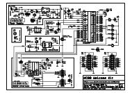
TinyARM PHIL40 LPC2103 <strong>Module</strong> v0.2<br />
Philips TinyARM PHIL40 <strong>Module</strong><br />
1. Introduction<br />
The purpose of this document is to specify mechanical dimensions and<br />
electrical behavior of TinyARM LPC2103 PHIL40 module.<br />
2. Reason for development<br />
Philips introduced LPC2103 processor housed in LQFP 48 pin package.<br />
It features 32kbyte Flash memory and 8kbyte SRAM. This chip can be<br />
used as a replacement for 8/16 microcontrollers.<br />
There are following problems when using this chip:<br />
A. Price of development tools, both software and hardware.<br />
B. Unusual package which is not convenient for development.<br />
C. The chip requires 2 different voltages.<br />
D. Battery voltage (for RTC and RAM backup) range is not sufficient.<br />
3. Solution<br />
PHIL40 module intends to solve all problems:<br />
A. The module is housed in DIP40 package which has pin out similar<br />
to 8751 microcontroller.<br />
B. The module requires just one convenient 5V supply. All the<br />
voltages<br />
for Philips LPC2103 processor are generated on-board. The module<br />
can supply 1.8V and 3.3V supply to external (low power) circuitry.<br />
C. The module features built-in 10 MHz oscillator.<br />
D. The module includes Reset generator.<br />
E. The module includes 32768Hz quartz and backup voltage generation<br />
for real time clock section of the processor.<br />
F. The module is re-usable. It can be used in several designs, the<br />
only<br />
additional investment is DIL40 socket for each design.<br />
F. Software tools are either IAR or free GNU .<br />
4. List of required signals for development version<br />
All the signals required for standard ARM Test/Debug <strong>JTAG</strong> interface<br />
are<br />
generated on PHIL40 board. This includes standard <strong>JTAG</strong> TRSTN,TCLK,<br />
TMS,TDI and TDO signals and handling of RTCK and DBGSEL signals.<br />
Reset signal for all circuitry is generated on board.<br />
5. Voltage levels and electrical behaviour<br />
PHIL40 module runs from 5V supply applied to DIL40 pin 40.<br />
The supply voltage for this version can be from 4.5V to 5.5V.<br />
The estimated current consumption is 100mA from 5V supply.<br />
PHIL40 module can supply 1.8 and 3.3V voltage from pins located in<br />
the middle of the board. Do not draw more than 20mA from any supply !<br />
Voltage levels for ARM I/O pins are 3.3V compliant. The specs says<br />
that<br />
I/O pins are 5V tolerant.<br />
6. Method of programming internal Flash<br />
There are 2 methods to program Flash – either <strong>JTAG</strong> or <strong>ISP</strong> (using<br />
UART0 of Philips LPC210x chip). Please, refer to the relevant Philips<br />
LPC210x<br />
manual.<br />
Note: P0.14 must be logic low for LPC2103 processor to enter boot<br />
loader mode. For normal operation, use pull up resistor to 3.3V<br />
1
TinyARM PHIL40 LPC2103 <strong>Module</strong> v0.2<br />
so that PHIL40 does not enter boot loader mode.<br />
7. Mechanical dimensions<br />
The module should fit into the standard 600 mils DIL40 socket.<br />
8. Tips and tricks for development<br />
None<br />
9. Preliminary drawing<br />
None<br />
10. PHIL40 board control signals<br />
RSTN – input for external reset signal, active low. Leave unconnected<br />
if not used. PHIL40 board generates proper internal Reset signal upon<br />
power-up. An external push button can be connected to RSTN to<br />
generate<br />
reset signal. No debounce is needed for the push button.<br />
Note: If driving RSTN pin by external circuitry, then it must be open<br />
collector (open drain) with pull-up resistor. Do NOT use push-pull<br />
to drive RSTN !<br />
RST_OUTN – output of PHIL40 internal reset generator, active low,<br />
open<br />
drain output.<br />
PWRENN – input controlling PHIL40 voltage regulators. Default is low<br />
when the voltage regulators are enabled and generate 3.3V and 1.8V<br />
respectively. This signal is pulled down on PHIL40 board. Normally<br />
leave this pin unconnected (N.C.). Driving this pin high will disable<br />
voltage regulators.<br />
DBGSEL – this is Debug Select input. Default is low when the part<br />
operates normally, executing code in internal Flash or SRAM.<br />
Leave this pin unconnected for normal operation as it is pulled down<br />
by 10k resistor on the module. Drive this pin high if there is a need<br />
to enter Debug Mode.<br />
RTCK – leave this pin unconnected for normal operation.<br />
BATT – connect an external battery for RTC section backup.<br />
11. Interfacing PHIL40 board to various voltage levels<br />
PHIL40 board runs from 5V supply and generates 3.3V voltage for I/O<br />
pins logic levels reference. All PHIL40 I/Os are 3.3V compliant,<br />
meaning they can directly interface with 3.3V logic. They can also<br />
interface directly 5V LV TTL and HCT MOS logic.<br />
PHIL40 I/Os are 5V resistant so they can receive 5V TTL/HC/HCT logic<br />
levels. However, I/O cannot drive 5V HC MOS inputs directly, some<br />
level<br />
conversion is necessary. The simplest method for slow signals is<br />
using<br />
pull up resistor to 5V supply.<br />
2
TinyARM PHIL40 LPC2103 <strong>Module</strong> v0.2<br />
12. Simple test / First use of TinyARM<br />
It is easy to start with PHIL40 module. All what you need is and<br />
experimental board, DIL40 socket, RS232 interface circuit like MAX232<br />
and 5V power supply. Philips supplies LPC210x <strong>ISP</strong> utility for Windows<br />
which can talk to PHIL40 UART0 serial interface.<br />
Make the connections like the following:<br />
- connect ground to DIL40 pin 20<br />
- connect +5V to DIL40 pin 40<br />
- connect logic low (pull down 3k9 to ground) to DIL40 pin 16 which<br />
corresponds to PHIL40 Port0.14. This pin is samples during reset<br />
or<br />
power-up to indicate whether to start <strong>ISP</strong> utility.<br />
- connect DIL40 pin 1 which corresponds to PHIL40 Port00/TxD0 to the<br />
input of MAX232 driver, e.g. to T1in (MAX232 pin 11). The output<br />
of MAX232 driver, e.g. T1out (MAX232 pin 14) is connected to DB9<br />
or DB25 connector as TxD signal.<br />
- connect DIL40 pin 2 which corresponds to PHIL40 Port01/RxD0 to the<br />
output of MAX232 receiver, e.g. to R1out (MAX232 pin 12). The<br />
input of MAX232 driver, e.g. R1in (MAX232 pin 13) is connected to<br />
DB9 or DB25 connector as RxD signal.<br />
- Connect a push-button between DIL40 pin 9 RSTN and ground.<br />
- Insert PHIL40 board into DIL40 socket.<br />
- Connect RS232 cable to the PC on one side and to your board on the<br />
other side.<br />
- Apply power from 5V supply.<br />
- Start Philips LPC210x utility<br />
- Press push button to connect PHIL40 to the PC, if necessary.<br />
- ENJOY !<br />
13. Connecting Macraigor Systems WIGGLER to TinyARM board<br />
The easiest way is to use extra DIL40 socket and connect DIL40 pins<br />
to the male dual-row 20 pin header as follows:<br />
DIL40 pin Header pin Signal name<br />
20 4,6,8,10,12,14 GND<br />
16,18,20<br />
22 3 TRSTN<br />
23 7 TMS<br />
24 9 TCK<br />
25 5 TDI<br />
26 13 TDO<br />
9 15 RESETN<br />
30 11 RTCK<br />
42 1,2 VCC (3.3V)<br />
Some additional resistors are strongly recommended to apply correct<br />
default voltage levels on <strong>JTAG</strong> pins.<br />
Notes:<br />
a. DBGSEL pin should be driven high, i.e. pull up resistor 1k to Vcc<br />
for the part to enter debug mode when debugging is possible.<br />
b. PHIL40 module can supply 1.8V and 3.3V voltage to other (low<br />
power)<br />
peripherals.<br />
3
TinyARM PHIL40 LPC2103 <strong>Module</strong> v0.2<br />
14. TinyARM board pinout<br />
Pin Nr. Pin Name Altern. Pin Nr. Pin Name Altern.<br />
1 P0.0 TxD0/PWM1 40 VCC 5V<br />
2 P0.1 RxD0/PWM3 39 P0.31 EXTIN0/*<br />
3 P0.2 SCL/CAP0.0 38 P0.30 TRACEPKT3/*<br />
4 P0.3 SDA/MAT0.0 37 P0.29 TRACEPKT2/*<br />
5 P0.4 SCK/CAP0.1 36 P0.28 TRACEPKT1/*<br />
6 P0.5 MISO/MAT0.1 35 P0.27 TRACEPKT0/*<br />
7 P0.6 MOSI/CAP0.2 34 P0.26 TRACESYNC<br />
8 P0.7 SSEL/PWM 33 P0.25 PIPESTAT2<br />
9 RSTN 32 P0.24 PIPESTAT1<br />
10 P0.8 TxD1/PWM4 31 RSTN_OUT<br />
11 P0.9 RxD1/PWM6 30 RTCK<br />
12 P0.10 RTS1/CAP1.0 29 DBGSEL<br />
13 P0.11 CTS1/CAP1.1 28 P0.23 PIPESTAT0<br />
14 P0.12 DSR1/MAT1.1 27 P0.22 TRACECLK<br />
15 P0.13 DTR1/MAT1.1 26 P0.21 PWM5/TDO<br />
16 *Note P0.14 DCD1/EINT1 25 P0.20 MAT1.3/TDI<br />
17 P0.15 RI1/EINT2 24 P0.19 MAT1.2/TCK<br />
18 PWRENN 23 P0.18 CAP1.3/TMS<br />
19 VBAT 22 P0.17 CAP1.2/TRST<br />
20 GND 21 P0.16 EINT0/MAT0.2<br />
Note: P0.14 must be logic low for PHIL40 to enter boot loader mode.<br />
15. Known problems of Philips LPC2106 processor<br />
(Check if this applies to LPC2103 !!!!)<br />
a. External interrupts 0 to 2 (EINT0 to EINT2) are level sensitive.<br />
It is not possible to set them to edge sensitive mode.<br />
b. SPI interface requires to use pull up resistor on SSEL pin even<br />
if it is set to Master mode. That results in pin wasting, pin SSEL<br />
cannot be used as GPIO P0.7 when SPI is used.<br />
4


![mbed NXP LPC11U24 Schaltplan 010.2 [PDF/57KB]](https://img.yumpu.com/43869567/1/190x135/mbed-nxp-lpc11u24-schaltplan-0102-pdf-57kb.jpg?quality=85)