SuperFASTCOM HARDWARE MANUAL - Commtech-fastcom.com
SuperFASTCOM HARDWARE MANUAL - Commtech-fastcom.com
SuperFASTCOM HARDWARE MANUAL - Commtech-fastcom.com

You also want an ePaper? Increase the reach of your titles
YUMPU automatically turns print PDFs into web optimized ePapers that Google loves.
9011 E. 37TH STREET N.<br />
WICHITA, KANSAS 67226-2006<br />
(316) 636-1131<br />
FAX (316) 636-1163<br />
http://www.<strong>com</strong>mtech-<strong>fast<strong>com</strong></strong>.<strong>com</strong>/<br />
COPYRIGHT (C) 2001, 2002, 2003, 2004, 2005, 2010<br />
All rights reserved, including those to reproduce this document or parts thereof in<br />
any form without permission in writing from <strong>Commtech</strong>, Inc.<br />
FASTCOM and the “Alpha Lemur” are registered trademarks of <strong>Commtech</strong>, Inc.<br />
Microsoft is a registered trademark of Microsoft Corporation.<br />
WINDOWS is a trademark of Microsoft Corporation.
REVISION NOTES<br />
REVISION PAGE NUMBER CHANGES MADE<br />
2.1 12 Revised Windows 2000 test procedure<br />
2.2 20 Changed warranty to 2 years<br />
2.3 5 Added <strong>SuperFASTCOM</strong> Cable to packing<br />
list<br />
2.4 11 Added link to installation manual<br />
2.5 19 Updated contact information<br />
2.6 10 Removed RS-530 references<br />
2.7 1<br />
13<br />
Changed board revision level on CE<br />
certificate<br />
Removed unnecessary register setup<br />
information and repaginated<br />
2.8 1 Added SuperFast<strong>com</strong> family information<br />
2.9 18 Changed warranty period to lifetime<br />
2.10 12-13 Added more programs to list<br />
2.11 19-21 Added “Errata” section<br />
Modified features to agree with errata<br />
2.12 21 Appended to “Errata” section<br />
2.13 11 Add hardware installation notes 2a & 2b<br />
2.14 14 Added register offset descriptions<br />
2.15 23 Changed warranty to limited lifetime<br />
2.16 23 Updated Limitation of Liability
CONTENTS<br />
“CE” CERTIFICATE .............................................................................................................. 1<br />
INTRODUCTION<br />
Description / Block Diagram ............................................................................................ 3<br />
Specifications / Features ................................................................................................. 4<br />
Board Layout ................................................................................................................... 5<br />
Communications Overview.............................................................................................. 6<br />
Comparison to ESCC Family........................................................................................... 8<br />
CABLE<br />
Cable Configuration......................................................................................................... 9<br />
DB25 Connector Description ......................................................................................... 10<br />
INSTALLATION<br />
Hardware Installation..................................................................................................... 11<br />
Software Installation ...................................................................................................... 11<br />
TESTING THE INSTALLATION<br />
Windows 2000 Test Procedure...................................................................................... 11<br />
SOFTWARE UTILITIES...................................................................................................... 12<br />
PROGRAMMING................................................................................................................ 14<br />
MEMORY MANAGEMENT ................................................................................................. 16<br />
RS-422/485......................................................................................................................... 17<br />
Termination Resistance................................................................................................. 18<br />
PROGRAMMABLE CLOCK GENERATORS...................................................................... 19<br />
ERRATTA ........................................................................................................................... 20<br />
TECHNICAL SUPPORT ..................................................................................................... 23<br />
APPENDIX A<br />
Infineon 20534 Technical Data Sheet............................................................................ 24
1<br />
EUROPEAN UNION DECLARATION OF CONFORMITY<br />
Information Technology Equipment<br />
The Company COMMTECH, INC. declares under its own and full responsibility that the product<br />
" SuperFast<strong>com</strong> - Revision 2.0 "<br />
on which is attached this Certificate is <strong>com</strong>pliant to the "89/336/EEC" Directive, amended by 92/31/EEC and<br />
93/88/EEC.<br />
[ ] The product identified above <strong>com</strong>plies with the requirements of the above EU Directive by meeting the<br />
following standards:<br />
• EN 50081-1 (1992) EMC Generic Emission Standard - Part 1, Residential, Commercial and Light Industry<br />
- EN 55022 (1995), CISPR 22 (1993) Limits and Methods of Measurement of Radio Disturbance<br />
Characteristics of Information Technology Equipment, 30 MHz - 1 GHz, Class B Limits<br />
• EN 50082-1 (1992) EMC Generic Immunity Standard - Part 1, Residential, Commercial and Light Industry<br />
- IEC 801-2 (1984), Method of Evaluating Susceptibility to Electrostatic Discharge, Level 4<br />
- IEC 801-3 (1984), Radiated Electromagnetic field Requirements, Level 3<br />
- IEC 801-4 (1988), Electrical Fast Transient/Burst Requirements, Level 2<br />
Products listed on this declaration are exempt from the requirements of the 73/23/EEC directive due to the input<br />
voltage specification as stated in Article 1 of the directive.<br />
The technical documentation required to demonstrate that this product meets the requirements of the EMC Directive<br />
has been <strong>com</strong>piled by the signatory below and is available for inspection by the relevant enforcement authorities.<br />
In WICHITA, KS on December 31st of 1995<br />
9011 E. 37th Street North<br />
Wichita, KS 67226-2006<br />
(316) 636-1131<br />
Fax (316) 636-1163<br />
Mr. Glen R. Alvis<br />
Chief Engineer
3<br />
INTRODUCTION<br />
The new <strong>SuperFASTCOM</strong> PCI adapter is a very high-speed, four channel, synchronous serial<br />
<strong>com</strong>munications adapter designed for Windows- and LINUX-based industrial/<strong>com</strong>mercial<br />
systems. Its outstanding features include data rates up to 40 Mbits/s and the ability to buffer<br />
up to 4 Gigabytes of data (Windows 2000) in system memory.<br />
The <strong>SuperFASTCOM</strong> supports standard synchronous protocols (HDLC, SDLC) and their<br />
variations, as well as standard asynchronous data formats at data rates up to 40 Mbits/s. The<br />
on-board clock generator provides a high-speed clock source for your system and<br />
eliminating the need for an external clock. The board also features high-speed RS-422/RS-<br />
485 drivers/receivers with on-board line termination.<br />
Programming is simplified with the inclusion of drivers, example programs and <strong>com</strong>prehensive<br />
documentation supplied on the Fast<strong>com</strong> CD. The <strong>SuperFASTCOM</strong> provides high speed and<br />
high reliability while greatly reducing development time and system <strong>com</strong>plexity.<br />
The <strong>SuperFASTCOM</strong> family includes:<br />
Form Factor Line Type Ports<br />
PCI RS422/485 OR RS232 4<br />
PC/104+ RS422/485 1 or 2<br />
CompactPCI RS422/485 4<br />
CompactPCI Rear IO RS422/485 4<br />
The following diagram illustrates the basic structure of the <strong>SuperFASTCOM</strong>:<br />
Programmable High Speed Clock Source<br />
Status<br />
LEDs<br />
Clock<br />
Generator<br />
#2<br />
Clock<br />
Generator<br />
#1<br />
Communication<br />
Processor<br />
Memory<br />
Controller<br />
Bus Control<br />
Logic<br />
Drivers/<br />
Receivers<br />
Termination<br />
Resistance<br />
1<br />
2<br />
3<br />
4<br />
Channels<br />
PCI Bus
4<br />
SPECIFICATIONS:<br />
COMMUNICATION CONTROLLER: INFINEON 20534<br />
OS SUPPORT:<br />
Windows XP, 2000, NT4; Linux<br />
DATA RATE:<br />
All baud rates up to 40 Mbps<br />
DATA BUFFERING:<br />
Up to 4 Gbytes (Windows)<br />
Up to 52 Mbytes per channel (LINUX)<br />
DRIVERS/RECEIVERS:<br />
High Speed RS-422/RS-485<br />
SIGNALS:<br />
TxD, RxD, RTS, CTS, DCD, TT, RT, ST<br />
CONNECTOR CONFIGURATION: DB-78 to four DB-25 connectors<br />
BUS INTERFACE: 32-bit PCI Ver. 2.1<br />
POWER REQUIREMENTS:<br />
450mA @ +5 (typical)<br />
ENVIRONMENT:<br />
Operating Temperature Range: 0 to 70 C<br />
Humidity:<br />
0 to 90% (non-condensing)<br />
MEAN TIME BETWEEN FAILURES: 24.61 Yrs<br />
CERTIFICATION:<br />
FCC <strong>com</strong>pliant, CE marked<br />
FEATURES:<br />
Four independent channels<br />
Status LEDs for system development/debugging<br />
Two programmable on-board clock generators<br />
“Switchless” design for durability and reliability<br />
Hardware documentation and software included on CD<br />
Made in Wichita, KS U.S.A.
5<br />
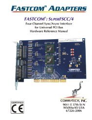
<strong>SuperFASTCOM</strong><br />
BOARD LAYOUT<br />
TRANSMIT/<br />
RECEIVE<br />
STATUS<br />
LEDs<br />
DB78<br />
CONNECTOR<br />
<strong>Commtech</strong>, Inc.<br />
Wichta, KS<br />
PACKING LIST:<br />
<strong>SuperFASTCOM</strong> Card<br />
<strong>SuperFASTCOM</strong> Cable<br />
FASTCOM CD<br />
If an omission has been made, please call technical support for a replacement.
6<br />
COMMUNICATIONS OVERVIEW<br />
• HDLC/SDLC Protocol Modes<br />
- Automatic flag detection and transmission<br />
- Shared opening and closing flag<br />
- Generation of interframe-time fill ’1’s or flags<br />
- Detection of receive line status<br />
- Zero bit insertion and deletion<br />
- CRC generation and checking (CRC-CCITT or CRC-32)<br />
- Transparent CRC option per channel and/or per frame<br />
- Programmable Preamble (8 bit) with selectable repetition rate<br />
- Error detection (abort, long frame, CRC error, short frames)<br />
• Bit Synchronous PPP Mode<br />
- Bit-oriented transmission of HDLC frame (flag, data, CRC, flag)<br />
- Zero bit insertion/deletion<br />
- 15 consecutive ’1’ bits aborts sequence<br />
• Octet Synchronous PPP Mode<br />
- Octet-oriented transmission of HDLC frame (flag, data, CRC, flag)<br />
- Programmable character map of 32 hard-wired characters (00 H -1F H)<br />
- Four programmable characters for additional mapping<br />
- Insertion/deletion of control-escape character (7D H) for mapped characters<br />
• Asynchronous (ASYNC) Protocol Mode<br />
- Selectable character length (5 to 8 bits)<br />
- Even, odd, forced or no parity generation/checking<br />
- 1 or 2 stop bits<br />
- Break detection/generation<br />
- In-band flow control by XON/XOFF<br />
- Immediate character insertion<br />
- Termination character detection for end of block identification<br />
- Time out detection<br />
- Error detection (parity error, framing error)<br />
• BISYNC Protocol Mode<br />
- Programmable 6/8-bit SYN pattern (MONOSYNC)<br />
- Programmable 12/16-bit SYN pattern (BISYNC)<br />
- Selectable character length (5 to 8 bits)<br />
- Even, odd, forced or no parity generation/checking<br />
- Generation of interframe-time fill ’1’s or SYN characters<br />
- CRC generation (CRC-16 or CRC-CCITT)<br />
- Transparent CRC option per channel and/or per frame<br />
- Programmable Preamble (8 bit) with selectable repetition rate<br />
- Termination character detection for end of block identification<br />
- Error detection (parity error, framing error)<br />
• Extended Transparent Mode<br />
- Fully bit transparent (no framing, no bit manipulation)<br />
- Octet-aligned transmission and reception<br />
• Protocol and Mode Independent<br />
- Data bit inversion
7<br />
- Data overflow and under run detection<br />
- Timer<br />
Protocol Support<br />
• Address Recognition Modes<br />
- Mode 0 - No address recognition<br />
- Mode 1 - 8-bit (high byte) address recognition<br />
- Non-Auto Mode - 8-bit (low byte) or 16-bit (high and low byte) address recognition<br />
General<br />
• On-chip Rx and Tx data buffer (the buffer size is 128 32-bit words each)<br />
• Programmable buffer size in transmit direction per channel; buffer allocation in receive<br />
direction on request.<br />
• Programmable watermark for receive channels to control transfer of receive data to<br />
host memory.<br />
• Two programmable watermarks for each transmit channel, i.e. one controlling data<br />
loading from host memory and one controlling transfer of transmit data to the<br />
corresponding Serial Communication Controller (SCC).<br />
• Internal test loop capability.
8<br />
<strong>SuperFASTCOM</strong> / ESCC FAMILY COMPARISON<br />
Enhancements to the ESCC Serial Core<br />
The <strong>SuperFASTCOM</strong> adapter contains the core logic of the ESCC2 V3.2A as the heart of the<br />
device. Some enhancements are incorporated in the <strong>SuperFASTCOM</strong>. These are:<br />
• 16-Kbyte packet length byte counter<br />
• Enhanced address filtering (16-bit maskable)<br />
• Enhanced time slot assigner<br />
• Support of high data rates (45 Mbit/s for DS3 or 52 Mbit/s for OC1). Protocol support is<br />
limited to HDLC Sub-modes without address recognition.<br />
Simplifications of the ESCC Serial Core<br />
The following features of the ESCC core have been removed:<br />
• SDLC Loop mode<br />
• Extended transparent mode 0 (this mode provided octet buffered data reception without<br />
usage of FIFOs; the <strong>SuperFASTCOM</strong> supports octet buffered reception via appropriate<br />
threshold configurations for the SCC receive FIFOs)
9<br />
CONFIGURATION FOR <strong>SuperFASTCOM</strong> CABLE ASSEMBLY<br />
The cable provided with your SuperFast<strong>com</strong> adapter splits each channel from the DB78 to into<br />
four DB 25 male connectors.<br />
DB78 PIN NUMBER<br />
SIGNAL DB25 # CHANNEL 1 CHANNEL 2 CHANNEL 3 CHANNEL 4<br />
GND 1 58 38 9 48<br />
GND 7 68 29 10 49<br />
SD- 2 70 13 22 62<br />
SD+ 14 50 32 2 46<br />
RD- 3 73 36 6 65<br />
RD+ 16 53 17 26 42<br />
RTS- 4 71 33 3 63<br />
RTS+ 19 51 14 23 45<br />
CTS- 5 74 18 27 66<br />
CTS+ 13 54 37 7 41<br />
DCD- 10 76 31 8 40<br />
DCD+ 8 57 12 28 60<br />
TT- 11 69 30 1 61<br />
TT+ 24 52 11 21 47<br />
RT- 9 72 16 25 64<br />
RT+ 17 56 35 5 43<br />
ST- 12 75 34 4 67<br />
ST+ 15 55 15 24 44<br />
PRGCLK- 23 77 N/A N/A N/A<br />
PRGCLK+ 20 78 N/A N/A N/A
10<br />
<strong>SuperFASTCOM</strong> DB25<br />
CABLE CONNECTOR DESCRIPTION<br />
PIN DESCRIPTIONS<br />
CTS+<br />
ST-<br />
TT-<br />
DCD-<br />
RT-<br />
DCD+<br />
GND<br />
CTS-<br />
RTS-<br />
RD-<br />
SD-<br />
GND<br />
13<br />
12<br />
11<br />
10<br />
9<br />
8<br />
7<br />
6<br />
5<br />
4<br />
3<br />
2<br />
1<br />
25<br />
24<br />
23<br />
22<br />
21<br />
20<br />
19<br />
18<br />
17<br />
16<br />
15<br />
14<br />
TT+<br />
PROGCLK- (CH1)<br />
PROGCLK+ (CH1)<br />
RTS+<br />
RT+<br />
RD+<br />
ST+<br />
SD+<br />
PIN# DESCRIPTION 422 TYPE CONNECTED TO<br />
1 SHIELD/GROUND GND<br />
7 SIGNAL/GROUND GND<br />
2 TRANSMIT DATA A SD-<br />
14 TRANSMIT DATA B SD+<br />
3 RECEIVE DATA A RD-<br />
16 RECEIVE DATA B RD+<br />
4 REQUEST TO SEND A RTS-<br />
19 REQUEST TO SEND B RTS+<br />
5 CLEAR TO SEND A CTS-<br />
13 CLEAR TO SEND B CTS+<br />
CLOCK SIGNALS<br />
PIN# DESCRIPTION 422 TYPE CONNECTED TO<br />
8 DATA CARRIER DETECT A DCD+<br />
10 DATA CARRIER DETECT B DCD-<br />
24 TRANSMIT CLOCK OUT A TT+<br />
11 TRANSMIT CLOCK OUT B TT-<br />
17 RECEIVE CLOCK IN A RT+<br />
9 RECEIVE CLOCK IN B RT-<br />
15 TRANSMIT CLOCK IN A ST+<br />
12 TRANSMIT CLOCK IN B ST-<br />
Special Signals On Cable 1 Only<br />
Pin 20 PROGCLK + Programmable clock output<br />
Pin 23 PROGCLK-
11<br />
INSTALLATION<br />
Important: Observe Electrostatic Discharge (ESD) precautions when handling the<br />
<strong>SuperFASTCOM</strong> board.<br />
1. Unpack the <strong>SuperFASTCOM</strong> adapter. Keep the box and static bag for warranty repair<br />
returns.<br />
2. Select an open PCI slot in your PC.<br />
a. The SuperFast<strong>com</strong> requires that the selected PCI slot be capable of bus mastering.<br />
The card will not function correctly if installed into a non-bus mastering slot.<br />
b. If possible, install the SuperFast<strong>com</strong> into one of the Primary PCI slots. If you are<br />
installing into a Secondary PCI slot (i.e., on the other side of a PCI bridge), make sure<br />
that your motherboard’s PCI bridge is properly installed in your operating system<br />
before proceeding with the installation. If you do not have more than three PCI slots,<br />
then none of the slots are secondary.<br />
3. After removing the blank bracket from your PC, install the <strong>SuperFASTCOM</strong> in the PC by<br />
pressing it firmly into the slot. Install the bracket screw to hold it firmly in place.<br />
4. Re-install the cover on your PC.<br />
5. Install the <strong>SuperFASTCOM</strong> cable.<br />
Software Installation<br />
Select the link above to open the Installation Manual. Under SuperFast<strong>com</strong>, select your<br />
operating system and follow the instructions. When you are finished, select SuperFast<strong>com</strong><br />
from the list at the end of the SuperFast<strong>com</strong> section to return to this manual.<br />
TESTING THE INSTALLATION<br />
To fully test the installation of your SuperFast<strong>com</strong>, you will<br />
need to build a "loop back plug". Materials needed are a<br />
DB25 female receptacle (solder cup style) and a few short<br />
pieces of 20 or 24 AWG stranded wire. Jumper the pins<br />
together on the DB25 as illustrated:<br />
WINDOWS 2000 TEST PROCEDURE<br />
1. Place the loop back plug onto the Port 1 connector.<br />
1<br />
2<br />
3<br />
4<br />
5<br />
6<br />
7<br />
8<br />
9<br />
10<br />
11<br />
12<br />
13<br />
14<br />
15<br />
16<br />
17<br />
18<br />
19<br />
20<br />
21<br />
22<br />
23<br />
24<br />
25<br />
SIGNALS<br />
2 SD-<br />
3 RD-<br />
7 GND<br />
9 RT-<br />
10 DCD-<br />
11 TT-<br />
14 SD+<br />
16 RD+<br />
17 RT+<br />
24 TT+
12<br />
2. Open a console/DOS window.<br />
3. Change directories to where you installed/copied the software.<br />
4. Execute: setclock 0 4000000<br />
5. Execute: sfcset 0 hdlcset<br />
6. Execute: loopback 0 h<br />
The green and red LEDs for port 1 should be blinking/on. Wait a few moments, press a key,<br />
and the errors/number of bytes sent through the loop will be displayed. The numbers will vary<br />
depending on how long you allow the test to run<br />
The rest of the ports can be checked by executing:<br />
sfcset 1 hdlcset<br />
loopback 1 h<br />
sfcset 2 hdlcset<br />
loopback 2 h<br />
sfcset 3 hdlcset<br />
loopback 3 h<br />
SOFTWARE UTILITIES<br />
These programs and their source can be found on the Fast<strong>com</strong> CD or downloaded from<br />
our website at http://www.<strong>com</strong>mtech-<strong>fast<strong>com</strong></strong>.<strong>com</strong>/. They are meant to be used as<br />
educational tools and programming references when designing your own software.<br />
• sfcset.exe Use to change register settings in conjunction with the hdlcset file<br />
• hdlcset, asyncset, bisyncset<br />
Generic settings files to be used with sfcset.exe<br />
• getclock.exe returns programmable clock #1 rate (osc)<br />
• getclock2.exe returns programmable clock #2 rate (progclk +/-)<br />
• setclock.exe sets the programmable clock #1 (osc)<br />
• setclock2.exe sets the programmable clock #2 (prograclk +/-)<br />
• loopback.exe user program to effect a loopback on a SuperFast<strong>com</strong> channel<br />
• sfcmfc.exe<br />
o Install your loopback plug onto the SuperFast<strong>com</strong>.<br />
o Run “sfcmfc.exe”.<br />
o Select “connect” from the menu.<br />
o A dialog will open. Select the port to use (0,1,2,3).<br />
o Click on “OK”.<br />
o An info box will open; click “OK”.
13<br />
o Type a message: “Hello, world”.<br />
o What you type should show up under “Transmit” in the window.<br />
o Select “Send” from the menu.<br />
o The message will appear in red under “Received”.<br />
o To open a different port, either select “File->New” or “Disconnect” from the menu.<br />
• readlb.exe user program to read a SuperFast<strong>com</strong> special register<br />
• writelb.exe user program to read a SuperFast<strong>com</strong> special register<br />
• readreg.exe user program to read a 20534 register<br />
• writereg.exe user program to write to a 20534 register<br />
• send.exe user program that opens a file and sends it through port 0<br />
• flushrx.exe user program to flush the <strong>SuperFASTCOM</strong> receiver/buffers<br />
• flushtx.exe user program to flush the <strong>SuperFASTCOM</strong> transmitter/buffers<br />
• getbufs.exe user program to get buffering/descriptor parameters for a port<br />
• setbufs.exe user program to set buffering/descriptor parameters for a port<br />
• getclock.exe user program to get the current clock generator settings<br />
• getclock2.exe user program to get the current program clock generator settings<br />
• read_file_hdlc.exe user program to read hdlc frames from a port and stuff them to a<br />
file<br />
• sendfile.exe user program to send a file out a SuperFast<strong>com</strong> port<br />
• setchecktimeout.exe<br />
user mode function to set the timeout timer in the driver<br />
that checks for frames to be returned or sent<br />
• setfs6131clock.exe user program that sets the fs6131 clock generator which is only<br />
valid if you have an extended temperature card with fs6131’s on it<br />
• setrfi.exe user program to mask/unmask the frame end interrupt indication for<br />
receive descriptors<br />
• setrirq.exe user program to set the interrupt rate for receive descriptors<br />
• settirq.exe user program to set the interrupt rate for transmit descriptors<br />
• settfi.exe user program to mask/unmask the frame end interrupt indication for<br />
transmit descriptors<br />
• simuln200.exe user program to generate 26 byte hdlc frames simulating an LN200<br />
• st_tt.exe user program to switch the onboard txclk multiplexer between the<br />
TT output and the ST input<br />
• status.exe user program to read status from a SuperFast<strong>com</strong> port
14<br />
PROGRAMMING<br />
Refer to the enclosed FASTCOM CD for example programs, product updates, and software for<br />
testing your installation. Refer to the Infineon PEB 20534 User's Manual for register<br />
information.<br />
Local Bus Interface for PEB 20534 - Byte accesses<br />
Register at offset 0<br />
Channel 1<br />
Bit 0<br />
1 = receive constantly enabled<br />
0 = receive enabled only when RTS is off<br />
Bit 1<br />
1 = transmit constantly enabled<br />
0 = transmit enabled only when RTS is on<br />
Bit 2<br />
1 = TT constantly enabled<br />
0 = TT enabled only when RTS is on<br />
Bit 3 No function<br />
Channel 2<br />
Bit 4<br />
1 = receive constantly enabled<br />
0 = receive enabled only when RTS is off<br />
Bit 5<br />
1 = transmit constantly enabled<br />
0 = transmit enabled only when RTS is on<br />
Bit 6<br />
1 = TT constantly enabled<br />
0 = TT enabled only when RTS is on<br />
Bit 7 No function<br />
Register at offset 1<br />
Channel 3<br />
Bit 0<br />
1 = receive constantly enabled<br />
0 = receive enabled only when RTS is off<br />
Bit 1<br />
1 = transmit constantly enabled<br />
0 = transmit enabled only when RTS is on<br />
Bit 2<br />
1 = TT constantly enabled<br />
0 = TT enabled only when RTS is on<br />
Bit 3 No function<br />
Channel 4<br />
Bit 4<br />
1 = receive constantly enabled<br />
0 = receive enabled only when RTS is off<br />
Bit 5<br />
1 = transmit constantly enabled<br />
0 = transmit enabled only when RTS is on<br />
Bit 6<br />
1 = TT constantly enabled<br />
0 = TT enabled only when RTS is on<br />
Bit 7 No function<br />
Register at offset 2<br />
Channel 1 Channel 3<br />
Bit 0<br />
0 = ST connected to TXCLK 0 = ST connected to TXCLK<br />
Bit 4<br />
1 = ST not connected<br />
1 = ST not connected<br />
Bit 1<br />
0 = TT connected to TXCLK 0 = TT connected to TXCLK<br />
Bit 5<br />
1 = TT not connected<br />
1 = TT not connected<br />
Channel 2 Channel 4<br />
Bit 2<br />
0 = ST connected to TXCLK 0 = ST connected to TXCLK<br />
Bit 6<br />
1 = ST not connected<br />
1 = ST not connected<br />
Bit 3<br />
0 = TT connected to TXCLK 0 = TT connected to TXCLK<br />
Bit 7<br />
1 = TT not connected<br />
1 = TT not connected<br />
Offset 0 & 1 – These bits are generally for choosing between 422 and 485 <strong>com</strong>munications.<br />
• Receive constantly enabled – (default) for RS-422 <strong>com</strong>munication<br />
• Receive enabled only when RTS is off – also Rx Echo Cancel; disables the receiver<br />
when transmitting so that you do not receive everything that you transmit when using 2-<br />
wire RS-485.<br />
• Transmit constantly enabled – (default) for RS-422 <strong>com</strong>munication<br />
• Transmit enabled only when RTS is on – turns off the transmitter when it is not actively<br />
sending data so that it does not contend with another transmitter on the data bus
15<br />
• TT constantly enabled – (default) for RS-422 <strong>com</strong>munications<br />
• TT enabled only when RTS is on – turns off the transmit clock when it is not actively<br />
sending data so that it does not contend with another transmitter on the clock bus<br />
Offset 2 – These bits are for setting the transmit clock direction. The PEB20534 has only one<br />
transmit clock pin that can be an input or an output using CCR0:TOE. If that pin is configured<br />
to be an output, then it must be connected to a line driver. If that pin is configured to be an<br />
input, then it must be connected to a line receiver. The ST pin is TxClk as an input and the TT<br />
pin is TxClk as an output.<br />
• ST connected to TxClk – TxClk connected to the ST input pin. Never set CCR0:TOE=1<br />
when setting this bit!<br />
• ST not connected to TxClk – (default) TxClk not connected to the ST input pin<br />
• TT connected to TxClk – (default) TxClk connected to the TT output pin<br />
• TT not connected to TxClk – TxClk not connected to the TT output pin.<br />
Note: It is possible to configure the TxClk pin as an input TOE=0, and connect it to both the<br />
TT and ST pins. This will allow the external clock from the ST pins to be outputted on the<br />
TT pins.
16<br />
MEMORY MANAGEMENT<br />
High-speed <strong>com</strong>munications requires that large amounts of transmitted/received data be<br />
buffered so as to prevent data loss and maintain data throughput. The <strong>SuperFASTCOM</strong> is<br />
designed to utilize system memory directly, bypassing the system processor. The<br />
<strong>SuperFASTCOM</strong> accesses system memory through high-speed PCI Bus Mastering, using its<br />
on-board bus master controller and supplied software. This procedure for direct memory<br />
access (DMA) is by far the fastest, most efficient method of handling the large amounts of data<br />
that high-speed <strong>com</strong>munications generates. Data is transferred to and from the<br />
<strong>SuperFASTCOM</strong> adapter at data bus speed. Buffering a high-speed data stream is critical in<br />
order to maintain data integrity and reliability, to avoid data loss, and to prevent data overrun.<br />
The <strong>SuperFASTCOM</strong> does all this with minimal system processor involvement, therefore there<br />
is no reduction in processor performance due to data <strong>com</strong>munication overhead.<br />
How it works - The user designates in his program how much system memory will be allocated<br />
to <strong>com</strong>munications: the more memory in your system, the more you can allocate to the<br />
<strong>com</strong>munication process. As data is received, the on-board <strong>com</strong>munication processor fills a<br />
small local buffer. When this is full, the bus master controller on the <strong>SuperFASTCOM</strong> transfers<br />
this data directly to system memory. The local buffer is reset and the process begins again.<br />
Transmitting data works in reverse; data from system memory is directly transferred to the<br />
local buffer on the <strong>SuperFASTCOM</strong>. When the local buffer is empty, new data from memory is<br />
directly transferred in. All of this occurs without slowing or interfering with the system<br />
processor.<br />
The high speed PCI Bus Mastering procedure for direct memory access provides the fastest,<br />
most efficient method of data transfer. It also improves efficiency and reduces the cost of the<br />
<strong>SuperFASTCOM</strong> board by eliminating the need for on-board memory or a processor.
17<br />
RS-422 / RS-485<br />
Most engineers have worked with RS-232 devices at least once in their career. If you have<br />
never worked with RS-422 or RS-485 devices, you will be pleased to know that working with<br />
the <strong>SuperFASTCOM</strong> is not much different from working with an RS-232 device.<br />
The RS-422 standard was developed to correct some of the deficiencies of RS-232. In<br />
<strong>com</strong>mercial and industrial applications, RS-232 has some significant problems. First, the cable<br />
length between RS-232 devices must be short (usually less than 50 feet at 9600 Baud).<br />
Second, many RS-232 errors are the result of cables picking up normal industrial electrical<br />
noises such as fluorescent lights, motors, transformers, and other EMF sources. Third, RS-<br />
232 data rates are functionally limited to 19.2K Baud. On the other hand, the newer RS-422<br />
standard makes cable lengths up to 5000 feet possible and is highly immune to most industrial<br />
noises. Data rates are also improved -- the <strong>SuperFASTCOM</strong> features data rates up to 40<br />
Mega Baud. These improvements were made possible by differentially driving and receiving<br />
the data as opposed to the single ended method employed by the RS-232 standard. With the<br />
RS-422 standard, the transmit signal (TX in RS-232) is a differential signal consisting of SD+<br />
and SD-; the receive signal (RX in RS-232) consists of RD+ and RD-.<br />
Another draw back of RS-232 is that more than two devices cannot share a single cable. This<br />
is also true of RS-422, and that's why the RS-485 standard was developed. RS-485 offers all<br />
of the benefits of RS-422 and also allows multiple units (up to 32) to share the same twisted<br />
pair. RS-485 is often referred to as a "multi-drop" or "two-wire, half duplex" network because<br />
the drivers (transmitters) and receivers share the same two lines. In fact, up to 32 stations can<br />
share the same "twisted pair". In order for an RS-485 system to work, only one driver<br />
(transmitter) can occupy the network at a time. This means that each station on the network<br />
must control the enabling/disabling of their drivers in order to avoid network conflicts. If two<br />
drivers engage the network at the same time, data from both will be corrupted. In RS-485<br />
mode, the receivers are always enabled.<br />
For a more detailed description of RS-422 and RS-485, we re<strong>com</strong>mend the following<br />
references:<br />
LINEAR AND INTERFACE CIRCUITS APPLICATIONS, Volume 2: Line Circuits,<br />
Display Drivers. By D.E. Pippenger and E. J. Tobaben. Published 1985 by Texas<br />
Instruments. ISBN-0-89512-185-9<br />
Note: This book may be difficult to find in a bookstore. The best place to get it is<br />
directly from Texas Instruments or from one their <strong>com</strong>ponent dealers. Publication #<br />
SLYA002.<br />
"Driver/Receiver Family Extends Data-Link Performance", ELECTRONIC PRODUCTS,<br />
January 15, 1985. By Dale Pippenger and Joe Miller
18<br />
TERMINATION RESISTANCE<br />
In both the RS-422 and the RS-485 mode, the receiver end of the cable between two stations<br />
must be terminated with a resistor equal to the characteristic impedance of the wire. This is to<br />
prevent signal reflections in the wire and to improve noise rejection. However, you do not<br />
need to add a terminator resistor to your cables when you use the SuperFast<strong>com</strong>. The<br />
termination resistance is built in. We have installed a terminator resistor for each receiver:<br />
between each RD+ and RD- and between CTS+ and CTS- for each channel.<br />
If you are using the SuperFast<strong>com</strong> in a multi-drop network, the termination resistor should be<br />
removed from all units except the first and last (see the RS-485 illustration below). Call for<br />
technical support if you need to modify the resistor. You may also order the SuperFast<strong>com</strong><br />
without the termination resistor installed (it is easier to add the resistor than to remove it).<br />
Observe the resistors in the following drawings and remember that they are built into the<br />
SuperFast<strong>com</strong>:
19<br />
PROGRAMMABLE CLOCK GENERATORS<br />
The SuperFast<strong>com</strong> features two Programmable Clock Generators. Each is a Cypress<br />
ICD2053B chip, which offers a fully user-programmable phase-locked loop clock pulse<br />
generator in a single 8-pin package. The output of the generator may be changed "on the fly"<br />
to any desired frequency value. The ability to dynamically change the output frequency adds a<br />
whole new degree of freedom for the designer.<br />
Why have two clock generators?<br />
The first clock generator (the OSC clock generator) provides the clock pulse to the PEB20534<br />
<strong>com</strong>munications processor chip. Its maximum frequency is 33MHz and is programmable via<br />
the GPP register (bits 8 and 9). The second clock generator (the PROGCLK clock generator)<br />
directly drives the PROGCLK+ and PROGCLK- output signals (PIN 20 and 23 on Cable #1).<br />
The PROGCLK has a maximum frequency of 40MHz and is programmable via the GPP<br />
register (bits 10 and 11). The PROGCLK is designed to provide a system wide high-speed<br />
clock pulse.<br />
For additional information on the Cypress ICD2053B, please review the data sheet.<br />
An important fact about the clock generator<br />
There is only one clock input line on the PEB 20534 <strong>com</strong>munications chip and it is connected<br />
to the OSC clock generator on the SuperFast<strong>com</strong> board. The OSC clock generator can be<br />
programmed from any channel (SFC, SFC1, SFC2, SFC3) but you are programming the same<br />
clock generator (the OSC clock generator) in each case. Just keep in mind that the baud rate<br />
generators are independent for each channel, but all four baud rate generators are fed from<br />
one clock source (the OSC clock generator). If you change the OSC clock generator rate you<br />
will change the input to the baud rate generators for all channels.<br />
If you have multiple baud rates that must be generated on multiple channels, you should select an OSC<br />
clock rate from which all of the required baud rates can be derived. Changing the OSC clock generator<br />
output will affect the baud rates of all channels!!!!
20<br />
ERRATA<br />
The errata listed below are known issues with the either Super<strong>fast<strong>com</strong></strong> board or the PEB20534<br />
controller itself. For more information regarding any of these issues, please contact<br />
<strong>Commtech</strong> technical support.<br />
• Serial Bus Configuration Timing Modes<br />
The SuperFast<strong>com</strong> was not designed to make use of Serial Bus Configuration timing<br />
modes 1 and 2. Do not attempt to configure CCR0:SC(2..0) to use these modes as<br />
they will not work correctly.<br />
• Maximum Value of Baudrate Generator<br />
The maximum value ’BRM’ in register BRR must not exceed M = 14 (the specified<br />
maximum value is M = 15). This limits the baud rate generator unit to frequency division<br />
factors in the range k = 1... 1,048,576, instead of k = 1... 2,097,152.<br />
• DPLL Algorithm for FM0, FM1 and Manchester Encoding<br />
Recovering the clock from an FM0-, FM1- or Manchester-encoded receive data stream<br />
using the DPLL circuitry is not working. The DPLL-asynchronous interrupt (PLLA)<br />
occurs continuously.<br />
• HDLC Mode: False Receive Status Byte<br />
The receive status byte RSTA belonging to an already received frame is overwritten by<br />
0x00 if the following two conditions are met:<br />
1. The interframe timefill number of ’1’ bits between the closing flag and the opening<br />
flag of the next frame is in the range of [1 - 5].<br />
2. The receive CRC checking mode is selected to transfer the receive CRC into the<br />
receive FIFO (CCR2:RCRC = ’1’).<br />
In all cases meeting the first condition, the number of ‘1’ bits is treated as an invalid<br />
HDLC frame. This frame is prevented from being reported or forwarded to the receive<br />
FIFO because of its invalid length. However the serial receive logic calculates a receive<br />
status byte RSTA = 0x00 (invalid frame).<br />
If the receive CRC is selected to be transferred to the receive FIFO (second condition),<br />
the receive status value of the previous valid frame is not yet transferred when<br />
calculating the invalid receive status byte. Thus the original receive status value is<br />
overwritten by 0x00 marking the previous frame as ’invalid’.<br />
Workaround: The error cannot occur if bit CCR2:RCRC is set to ’0’, i.e. receive CRC is<br />
not transferred to the receive FIFO. Otherwise (if CCR2:RCRC = ’1’) reception of less<br />
than 6 consecutive ’1’ bits as interframe timefill must be avoided. This can be achieved<br />
by the transmitter either selecting interframe timefill flag sequences or preamble<br />
transmission.<br />
• HDLC Mode: Transmission with Shared Flags<br />
If the shared flag option is enabled in HDLC mode via bit CCR1:SFLAG, the first byte of<br />
a frame might be replaced by a ’7E’ flag or ’FF’ octet on the transmit line, depending on<br />
the interframe time fill selection (bit CCR2:ITF). This leads to a damaged transmit<br />
frame.
21<br />
Workaround: It is re<strong>com</strong>mended to disable shared flag transmission by setting bit<br />
CCR1:SFLAG = ’0’.<br />
Note: Reception of frames with shared flags is always possible and neither<br />
affected by this erratum nor by setting of bit CCR1:SFLAG. Thus networking with<br />
other HDLC equipment supporting shared flags is not restricted.<br />
• Asynchronous PPP Mode: Reception<br />
In asynchronous PPP mode the SCC receiver expects a back-to-back stream of<br />
ASYNC characters. Once synchronized on the first ASYNC character the receiver<br />
expects further octets back-to-back in a fixed scheme determined by the (8, N, 1)<br />
character format. The receiver does not synchronize again on subsequent ASYNC<br />
characters.<br />
Workaround: Do not attempt to configure ASYNC PPP mode, to realize asynchronous<br />
PPP mode it is re<strong>com</strong>mended to configure the SCC in ASYNC mode, implementing<br />
CRC calculation and character mapping in software. Examples for fast CRC calculation<br />
and the character mapping specification are given in RFC 1662 (July 1994) document.<br />
• Extended Transparent Mode: Minimum Frame Length<br />
If the frame length in extended transparent mode is programmed to one, an XDU<br />
interrupt is generated with all its consequences (transmit SCC stops).<br />
Workaround: Frame lengths of 2 or more bytes should be used instead. If a 1-byte<br />
frame shall be sent, an idle character should be attached to it.<br />
• HDLC Automode: Full-duplex Operation<br />
In HDLC Automode the transmission of an I-frame might be spoiled by simultaneous<br />
reception of a frame, sometimes resulting in endless repetition of a byte or in failure of<br />
the responding S-frame. Then this channel does not respond autonomously to further<br />
reception events.<br />
Workaround: None. Do not use full-duplex Automode.<br />
• Command Execution (CEC) Status Bit Error With External Clocking<br />
In general the PEB20534 supports external clock gapping in any clock mode in which<br />
the internal transmit or receive clock is supplied via the dedicated RxClk and/or TxClk<br />
pins. If one of the clocks is externally gapped, the respective receive or transmit block<br />
remains in its current static condition until the clock signal is active again. Any<br />
<strong>com</strong>mand bit in register CMDR (e.g. ’XRES’ and ’RRES’) effects either the transmit or<br />
receive logic and <strong>com</strong>mand execution only depends on this block and its clock supply<br />
respectively. Nevertheless all <strong>com</strong>mands are forwarded to both transmit and receive<br />
block and <strong>com</strong>mand execution must be reported internally by both blocks to reset status<br />
bit STAR:CEC. Another <strong>com</strong>mand is only accepted if ’CEC’ bit is cleared.<br />
Example: The SCC is configured in clock mode 0a, a clock signal is provided at pin<br />
TxClk but pin RxClk is supplied with a constant value (no clock signal or gapped). A<br />
transmitter reset <strong>com</strong>mand applied by write access to register CMDR will be executed<br />
by the transmit block, but status bit ’CEC’ remains active afterwards, because the<br />
receive block cannot report <strong>com</strong>mand execution without clock supply. Any further<br />
<strong>com</strong>mand will be ignored while ’CEC’ bit is active.<br />
Workaround: Transmit and receive blocks must be supplied with clock signals in<br />
general. Because reset of the <strong>com</strong>mand execution (CEC) status bit might be delayed
22<br />
due to one of the clocks temporarily gapped, ’CEC’ status bit must be checked for ’0’<br />
before writing a <strong>com</strong>mand bit.<br />
• Carrier Auto-detect in HDLC Mode<br />
The carrier detect (CD) input pin is supposed to enable and disable reception in clock<br />
modes 0, 2, 3, 6 and 7. In HDLC/PPP mode this function is not working properly and<br />
thus should not be enabled with bit CCR1:CAS.<br />
• Receiver in Extended Transparent Mode Does Not Initialize<br />
When attempting to use Extended Transparent Mode (raw bits), it appears as though<br />
the receiver does not activate. It unclear whether this is a bug in the PEB20534 or<br />
whether it was done by design, but the port that will be receiving in Ext. Trans. Mode<br />
must be initialized in clock mode 1 with a clock present on the RT pins. It can then be<br />
switched to any other clock mode and will operate correctly.<br />
Workaround: If your configuration already uses an external receive clock, simply<br />
initialize the card in clock mode 1 (CCR0:CM2..CM0 = ‘001’) with a clock present on the<br />
RT pins and then change to whatever clock mode you wish to use. If you do not have<br />
an external clock, you can utilize the PROGCLK output pins that are located on the<br />
DB25 connector for port 1 at pins 20 and 23. Jumper the PROGCLK pins to the RT<br />
pins of your receiving port and initialize the card in clock mode 1.
23<br />
TECHNICAL SUPPORT<br />
<strong>Commtech</strong> provides extensive technical support and application suggestions. Most of the problems that occur with the<br />
<strong>SuperFASTCOM</strong> can be corrected by double-checking the switch positions, your cables and your program. We re<strong>com</strong>mend<br />
that you build the loop back plug that is described in the Programming section of this manual. With that plug, you can quickly<br />
isolate the problem to the board, cables, or software.<br />
If you still have unresolved questions, use the following procedure to get technical support:<br />
1. Call our Technical Support Staff at (316) 636-1131. They are on duty from 9:00 AM to 5:00 PM Central Time.<br />
2. Ask for technical support for the <strong>SuperFASTCOM</strong>. Be ready to describe the problem, your <strong>com</strong>puter system, your<br />
application, and your software.<br />
3. If necessary, our staff will give you an RMA number (Return Material Authorization). Use this number on the mailing<br />
label and in all references to your board. Put the board back in its static bag and in its box. Ship the board back to us<br />
as directed.<br />
4. If you prefer, you may FAX a description of the problem to us at (316) 636-1163, or we can be reached on the Internet<br />
at http://www.<strong>com</strong>mtech-<strong>fast<strong>com</strong></strong>.<strong>com</strong>/TechSupport.html or by email at techsupport@<strong>com</strong>mtech-<strong>fast<strong>com</strong></strong>.<strong>com</strong>.<br />
FASTCOM LIMITED LIFETIME WARRANTY<br />
<strong>Commtech</strong>’s entire FASTCOM product line is covered by a limited lifetime warranty against defects in workmanship. This<br />
warranty is available only to the original purchaser and only covers defects in our workmanship. Any FASTCOM board that is<br />
returned to <strong>Commtech</strong> will, at the option of <strong>Commtech</strong>, be repaired or replaced at no charge -- except for circumstances<br />
excluded by this warranty.<br />
A Return Materials Authorization (RMA) number must be obtained from <strong>Commtech</strong> before a return will be accepted. Please<br />
contact us via telephone or email to obtain an RMA number.<br />
You are responsible for shipping charges when you return a FASTCOM board to <strong>Commtech</strong>. We will pay the shipping<br />
charges to send the board back to you if a defect in workmanship is found. However, if no defect in workmanship is found, or<br />
the board is not found to be defective, or the any of the following warranty exclusions occur, you will be responsible for<br />
shipping charges both ways.<br />
Warranty Exclusions<br />
This warranty does not cover problems or damage resulting from, but not limited to, the following:<br />
1. Any modification, misuse, abuse, disassembly, misapplication, or unauthorized repair by anyone other than<br />
<strong>Commtech</strong>.<br />
2. Any improper operation, including any use not in accordance with any verbal product instructions or documentation.<br />
3. Connection to an improper voltage supply or ESD damage.<br />
4. Any other cause not related to workmanship.<br />
Non-Warranty Repairs<br />
We can provide a quote for non-warranty repairs upon request.<br />
If any <strong>Commtech</strong> product is damaged such that it cannot be repaired, you can return it to <strong>Commtech</strong> for replacement under<br />
our Non-Repairable Replacement policy, regardless of the cause of damage. <strong>Commtech</strong> will replace the unit at 60% of the<br />
then-current list price.<br />
Limitation of Liability<br />
<strong>Commtech</strong> shall not be liable for any special, incidental, indirect, or consequential damages whatsoever, including but not<br />
limited to loss of profits, revenue, or data (whether direct or indirect), or <strong>com</strong>mercial loss for breach of any express or implied<br />
warranty on your product even if <strong>Commtech</strong> has been advised previously of the possibility of such damages. <strong>Commtech</strong> does<br />
not warrant that its products will work in every system or every system configuration. We do not warrant that our products will<br />
be suitable for your application. If you are dissatisfied with our product, contact customer service to arrange for a return of our<br />
product and refund of your money. <strong>Commtech</strong>’s liability, in any case, is limited to the original product purchase price and is<br />
available to the original customer only.
24<br />
APPENDIX A<br />
INFINEON 20534<br />
TECHNICAL DATA