Melexis 90217 Datasheet
Melexis 90217 Datasheet
Melexis 90217 Datasheet

You also want an ePaper? Increase the reach of your titles
YUMPU automatically turns print PDFs into web optimized ePapers that Google loves.
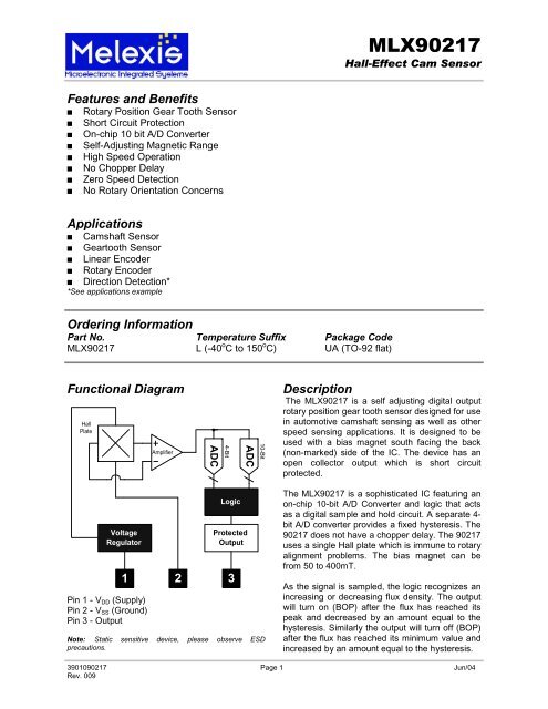
MLX<strong>90217</strong><br />
Hall-Effect Cam Sensor<br />
Features and Benefits<br />
■<br />
■<br />
■<br />
■<br />
■<br />
■<br />
■<br />
■<br />
Rotary Position Gear Tooth Sensor<br />
Short Circuit Protection<br />
On-chip 10 bit A/D Converter<br />
Self-Adjusting Magnetic Range<br />
High Speed Operation<br />
No Chopper Delay<br />
Zero Speed Detection<br />
No Rotary Orientation Concerns<br />
Applications<br />
■<br />
■<br />
■<br />
■<br />
Camshaft Sensor<br />
Geartooth Sensor<br />
Linear Encoder<br />
Rotary Encoder<br />
Direction Detection*<br />
■<br />
*See applications example<br />
Ordering Information<br />
Part No. Temperature Suffix Package Code<br />
MLX<strong>90217</strong> L (-40 o C to 150 o C) UA (TO-92 flat)<br />
Functional Diagram<br />
Hall<br />
Plate<br />
Amplifier<br />
ADC<br />
4-Bit<br />
ADC<br />
10-Bit<br />
Description<br />
The MLX<strong>90217</strong> is a self adjusting digital output<br />
rotary position gear tooth sensor designed for use<br />
in automotive camshaft sensing as well as other<br />
speed sensing applications. It is designed to be<br />
used with a bias magnet south facing the back<br />
(non-marked) side of the IC. The device has an<br />
open collector output which is short circuit<br />
protected.<br />
Voltage<br />
Regulator<br />
Pin 1 - V DD (Supply)<br />
Pin 2 - V SS (Ground)<br />
Pin 3 - Output<br />
Logic<br />
Protected<br />
Output<br />
1 2 3<br />
Note: Static sensitive device, please observe ESD<br />
precautions.<br />
The MLX<strong>90217</strong> is a sophisticated IC featuring an<br />
on-chip 10-bit A/D Converter and logic that acts<br />
as a digital sample and hold circuit. A separate 4-<br />
bit A/D converter provides a fixed hysteresis. The<br />
<strong>90217</strong> does not have a chopper delay. The <strong>90217</strong><br />
uses a single Hall plate which is immune to rotary<br />
alignment problems. The bias magnet can be<br />
from 50 to 400mT.<br />
As the signal is sampled, the logic recognizes an<br />
increasing or decreasing flux density. The output<br />
will turn on (BOP) after the flux has reached its<br />
peak and decreased by an amount equal to the<br />
hysteresis. Similarly the output will turn off (BOP)<br />
after the flux has reached its minimum value and<br />
increased by an amount equal to the hysteresis.<br />
39010<strong>90217</strong> Page 1 Jun/04<br />
Rev. 009
MLX<strong>90217</strong><br />
Hall-Effect Cam Sensor<br />
MLX<strong>90217</strong> Electrical Specifications<br />
DC Operating Parameters T A = -40 o C to 150 o C, V DD = 3.5V to 24V (unless otherwise specified).<br />
Parameter Symbol Test Conditions Min Typ Max Units<br />
Supply Voltage VDD Operating 3.5 - 24 V<br />
Supply Current IDD VDD = 12V 1.5 3.0 4.5 mA<br />
Supply Current IDD VDD = 3.5V to 24V 1 - 6 mA<br />
Leakage Current ILEAK VOUT = 3.5V to 24V - - 10 µA<br />
Output Current IOUT Operating - - 25 mA<br />
Output Saturation Voltage VSAT VDD = 12V, IOUT = 25mA - - 600 mV<br />
Output Short Circuit Current IFAULT Fault 50 100 150 mA<br />
Output Short Circuit Shutdown TFAULT Fault 100 - 200 µS<br />
Clock Frequency fCLK Operating 300 500 800 kHz<br />
Output Rise Time tr VDD=12V R1 = 880W C1 = 20pf - 400 nS<br />
Output Fall Time tf VDD=12V R1 = 880W C1 = 20pf - 400 nS<br />
Bandwidth BW Operating - - 15 kHz<br />
Thermal Resistance RTH Operating - - 200 oC/Watt<br />
MLX<strong>90217</strong> Magnetic Specifications<br />
DC Operating Parameters T A = -40 o C to 150 o C, V DD = 3.5V to 24V (Unless otherwise specified)<br />
Parameter Symbol Test Conditions Min Typ Max Units<br />
Back Bias Range BBIAS Operating -30 - 400 mT<br />
Linear Region VDD = 12V 50 - 500 mT<br />
Hysteresis Bhys VDD = 3.5V to 24V 1.8 3.5 10 mT<br />
Notes: 1 mT = 10 Gauss<br />
39010<strong>90217</strong> Page 2 Jun/04<br />
Rev. 009<br />
j
MLX<strong>90217</strong><br />
Hall-Effect Cam Sensor<br />
Performance Graphs<br />
Absolute Maximum Ratings<br />
Supply Voltage (Operating), VDD<br />
30V<br />
Supply Current (Fault), IDD<br />
50mA<br />
Output Current (Fault), IOUT<br />
30mA<br />
Output Current (Fault), Ifault<br />
50mA<br />
Output Voltage, VOUT<br />
30V<br />
Power Dissipation, PD<br />
100mW<br />
Operating Temperature Range, TA - 40°C to 150°C<br />
Storage Temperature Range, TS - 65°C to 150°C<br />
Maximun Junction Temp, TJ 175°C<br />
39010<strong>90217</strong> Page 3 Jun/04<br />
Rev. 009
MLX<strong>90217</strong><br />
Hall-Effect Cam Sensor<br />
Application Notes<br />
Maximum dynamic range is 500 mT. The<br />
hysteresis is fixed at 5.0 mT. Best angular<br />
accuracy will be obtained when the magnetic<br />
circuit provides peak magnetic flux at the chip<br />
near the high end of the linear range of 500 mT.<br />
EMC protection using external components are<br />
recommended. Two possibilities are shown on<br />
the following page. Normally the South pole faces<br />
the unbranded side of the device. A North pole<br />
will enable a test sequence used in factory<br />
testing.<br />
Unique Features<br />
The output is reset to the high state at power on<br />
(output driver is off) whatever the field is. The<br />
output only changes after the first min is detected.<br />
The reset state holds no information about the<br />
field. If the supply of the chip is raised slowly, the<br />
reset state is not stable. This has been observed<br />
at 0 field but it should be the same with small and<br />
large fields.<br />
Gear tooth sensors often need to be adjusted<br />
after the module is assembled to align the<br />
magnet with differential Hall plates or orient with<br />
teeth. However the MLX<strong>90217</strong> is “self adjusting”<br />
over a wide range of back bias flux eliminating<br />
the need for any trimming in the application. The<br />
magnet may be glued to the back surface (non<br />
branded side) of the IC using a cyanoacrylate<br />
adhesive or suitable epoxy.<br />
39010<strong>90217</strong> Page 4 Jun/04<br />
Rev. 009<br />
j
MLX<strong>90217</strong><br />
Hall-Effect Cam Sensor<br />
Applications Examples<br />
39010<strong>90217</strong> Page 5 Jun/04<br />
Rev. 009
MLX<strong>90217</strong><br />
Hall-Effect Cam Sensor<br />
Physical Characteristics<br />
39010<strong>90217</strong> Page 6 Jun/04<br />
Rev. 009<br />
j
MLX<strong>90217</strong><br />
Hall-Effect Cam Sensor<br />
Reliability Information<br />
This <strong>Melexis</strong> device is classified and qualified regarding soldering technology, solderability and<br />
moisture sensitivity level, as defined in this specification, according to following test methods:<br />
■<br />
■<br />
■<br />
■<br />
■<br />
■<br />
IPC/JEDEC J-STD-020<br />
Moisture/Reflow Sensitivity Classification For Nonhermetic Solid State Surface Mount Devices<br />
(classification reflow profiles according to table 5-2)<br />
EIA/JEDEC JESD22-A113<br />
Preconditioning of Nonhermetic Surface Mount Devices Prior to Reliability Testing<br />
(reflow profiles according to table 2)<br />
CECC00802<br />
Standard Method For The Specification of Surface Mounting Components (SMDs) of<br />
Assessed Quality<br />
EIA/JEDEC JESD22-B106<br />
Resistance to soldering temperature for through-hole mounted devices<br />
EN60749-15<br />
Resistance to soldering temperature for through-hole mounted devices<br />
MIL 883 Method 2003 / EIA/JEDEC JESD22-B102<br />
Solderability<br />
For all soldering technologies deviating from above mentioned standard conditions<br />
(regarding peak temperature, temperature gradient, temperature profile etc) additional classification<br />
and qualification tests have to be agreed upon with <strong>Melexis</strong>.<br />
The application of Wave Soldering for SMD’s is allowed only after consulting <strong>Melexis</strong> regarding<br />
assurance of adhesive strength between device and board.<br />
Based on <strong>Melexis</strong> commitment to environmental responsibility, European legislation<br />
(Directive on the Restriction of the Use of Certain Hazardous substances, RoHS) and customer<br />
requests, <strong>Melexis</strong> has installed a Roadmap to qualify their package families for lead free processes<br />
also.<br />
Various lead free generic qualifications are running, current results on request.<br />
For more information on manufacturability/solderability see quality page at our website:<br />
http://www.melexis.com/html/pdf/MLXleadfree-statement.pdf<br />
ESD Procautions<br />
Electronic semiconductor products are sensitive to Electro Static Discharge (ESD).<br />
Always observe Electro Static Discharge control procedures whenever handling semiconductor<br />
products.<br />
39010<strong>90217</strong> Page 7 Jun/04<br />
Rev. 009
MLX<strong>90217</strong><br />
Hall-Effect Cam Sensor<br />
Disclaimer<br />
Devices sold by <strong>Melexis</strong> are covered by the warranty and patent indemnification provisions appearing<br />
in its Term of Sale. <strong>Melexis</strong> makes no warranty, express, statutory, implied, or by description regarding<br />
the information set forth herein or regarding the freedom of the described devices from patent<br />
infringement. <strong>Melexis</strong> reserves the right to change specifications and prices at any time and without<br />
notice. Therefore, prior to designing this product into a system, it is necessary to check with<br />
<strong>Melexis</strong> for current information. This product is intended for use in normal commercial applications.<br />
Applications requiring extended temperature range, unusual environmental requirements, or high<br />
reliability applications, such as military, medical life-support or life-sustaining equipment are specifically<br />
not recommended without additional processing by <strong>Melexis</strong> for each application.<br />
The information furnished by <strong>Melexis</strong> is believed to be correct and accurate. However, <strong>Melexis</strong> shall<br />
not be liable to recipient or any third party for any damages, including but not limited to personal injury,<br />
property damage, loss of profits, loss of use, interrupt of business or indirect, special incidental<br />
or consequential damages, of any kind, in connection with or arising out of the furnishing, performance<br />
or use of the technical data herein. No obligation or liability to recipient or any third party shall<br />
arise or flow out of <strong>Melexis</strong>’ rendering of technical or other services.<br />
© 2002 <strong>Melexis</strong> NV. All rights reserved.<br />
For the latest version of this document, go to our website at:<br />
www.melexis.com<br />
Or for additional information contact <strong>Melexis</strong> Direct:<br />
Europe and Japan:<br />
All other locations:<br />
Phone: +32 13 67 04 95 Phone: +1 603 223 2362<br />
E-mail: sales_europe@melexis.com E-mail: sales_usa@melexis.com<br />
ISO/TS16949 and ISO14001 Certified<br />
39010<strong>90217</strong> Page 8 Jun/04<br />
Rev. 009<br />
j