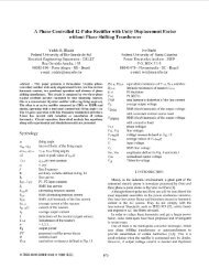
A Three-Phase Buck Rectifier with High-Frequency Isolation - Ivo Barbi
A Three-Phase Buck Rectifier with High-Frequency Isolation - Ivo Barbi
A Three-Phase Buck Rectifier with High-Frequency Isolation - Ivo Barbi

Create successful ePaper yourself
Turn your PDF publications into a flip-book with our unique Google optimized e-Paper software.
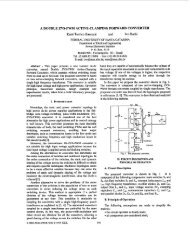
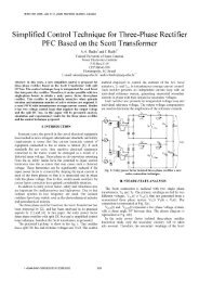
III. OPERATION STATES<br />
The operation states to a sextant of mains angular period<br />
is commented in this section. At each sextant 4 states can be<br />
always identified, in following figures the considered sextant<br />
is between 0 o and 60 o <strong>with</strong> states 1, 2 and 0 involved.<br />
Fig.3 the switches S2 and S3 are enable and the energy<br />
is transfer through transformer to load by Ds diode. Fig.4 the<br />
switches S1 and S2 are enable and the energy transfer through<br />
transformer to load is continued by Ds diode.<br />
iv ca<br />
D1n’<br />
D1p’<br />
Fig. 3.<br />
Ip<br />
D1p<br />
D2p<br />
D3p<br />
Ds Lo<br />
D2n’<br />
D3n’<br />
Ns<br />
Drl<br />
S1<br />
S2<br />
S3 Np<br />
Iv cb Iv cc<br />
D1n<br />
D2p’<br />
First state.<br />
D2n<br />
Estado1<br />
Ip<br />
D1p<br />
D2p<br />
D3p<br />
Ds Lo<br />
D1n’<br />
D2n’<br />
D3n’<br />
Ns<br />
Drl<br />
S1<br />
S2<br />
S3 Np<br />
iv ca Iv cb<br />
Iv cc<br />
D1p’<br />
D2p’<br />
D3p’<br />
D3p’<br />
D3n<br />
Nd<br />
Nd<br />
Dd<br />
Co<br />
Co<br />
Ro<br />
Ro<br />
IV. PROTOTYPE DESIGN AND IMPLEMENTATION<br />
In order to demonstrate the feasibility for the topology an<br />
experimental prototype was designed according the project set:<br />
V line−line = 220V ; f s =30kHz; P o =2.5kW; V o =48V .<br />
A. Input Filter Design<br />
An appropriate design of the AC input filter was carried<br />
out to provide a high power-factor, and T.H.D of line current<br />
intending to complain <strong>with</strong> IEC 61000-3-2 A Class, it was employed<br />
a classical low-pass LC filter which has a capacitance<br />
value defined according to the equation below:<br />
C f ≤<br />
2 · P o<br />
3 · η · ω · Vcf<br />
2 · tan(cos −1 (φ)) = 25μF (2)<br />
The presented parameters at equation 2 are defined as follow:<br />
V cf = 180V peak input filter capacitor voltage; η = 0.8<br />
estimated overall efficiency; φ =0, 99 estimated displacement<br />
factor and ω =2· π · f line frequency. It was decided by<br />
an Epcos polypropylene power capacitor C f = 22μF and<br />
defined a cut frequency for the input filter at 280Hz results<br />
an input filter inductance L s = 190μH.<br />
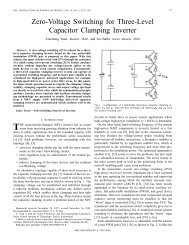
Fig. 4.<br />
D1n<br />
Second state.<br />
D2n<br />
Estado2<br />
D3n<br />
When the switches on the rectifier bridge are disenable the<br />
magnetization is extinct by Dd diode through the load in Fig.5.<br />
In order to assure a complete demagnetization a dead time is<br />
provided by a free-wheel current circulation in the end of 0<br />
state, see Fig.6.<br />
Dd<br />
B. Transformer Design<br />
The design procedure is based on usual equations to design<br />
E core high-frequency transformers where it was defined by<br />
following constrains parameters: ΔB =0.18T esla variation<br />
flux density ; J = 450 A<br />
cm<br />
current density; k 2<br />
p =0.7 winding<br />
fill factor; k w =0.4 spool factor.<br />
AeAw =<br />
2 · P o · 10 4<br />
k p · k w · J · f s · ΔB · η =98cm4 (3)<br />
D1p<br />
D2p<br />
D3p<br />
Ds Lo<br />
D1n’<br />
D2n’<br />
D3n’<br />
Ns<br />
Drl<br />
S1<br />
S2<br />
S3<br />
Np<br />
iv ca Iv cb<br />
Iv cc<br />
D1p’<br />
D2p’<br />
D3p’<br />
Nd<br />
D1n<br />
D2n<br />
D3n<br />
Dd<br />
Estado0<br />
Fig. 5. Demagnetization state.<br />
Co<br />
Ro<br />
It was selected a core E75/IP12 which were associated three<br />
cores in order to exceed the calculated AeAw at equation 3<br />
where it was obtained a AeAw = 125cm 4 and a total crosssectional<br />
area Ae =19.35cm 2 .<br />
The number of turns to each transformer winding are<br />
defined by the following equations where V retmax = 311V<br />
maximum rectified voltage; V retmin = 290V minimum rectified<br />
voltage; D M =0.5 maximum duty cycle and D =0.3<br />
average duty cycle:<br />
D1p<br />
D2p<br />
D3p<br />
Ds Lo<br />
D1n’<br />
D2n’<br />
D3n’<br />
Ns<br />
Drl<br />
S1<br />
S2<br />
S3<br />
Np<br />
iv ca Iv cb<br />
Iv cc<br />
D1p’<br />
D2p’<br />
D3p’<br />
Nd<br />
D1n<br />
D2n<br />
D3n<br />
Dd<br />
Co<br />
Ro<br />
N p = V ret min · 10 4<br />
2 · Ae · ΔB · f s<br />
=14turns (4)<br />
N s =1.1 · Np · (V o +1.5 · D)<br />
D · V retmin<br />
=9turns (5)<br />
Fig. 6.<br />
Free-wheel state.<br />
Estado0<br />
N d = N p ·<br />
V o<br />
V retmax<br />
· (1 − D M )<br />
D M<br />
=2turns (6)<br />
1130<br />
Authorized licensed use limited to: UNIVERSIDADE FEDERAL DE SANTA CATARINA. Downloaded on November 13, 2009 at 06:41 from IEEE Xplore. Restrictions apply.