SA Technical Datasheet v2.1
SA Technical Datasheet v2.1
SA Technical Datasheet v2.1

You also want an ePaper? Increase the reach of your titles
YUMPU automatically turns print PDFs into web optimized ePapers that Google loves.
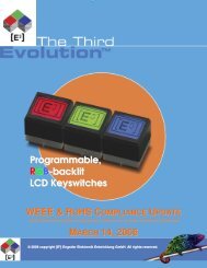
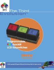
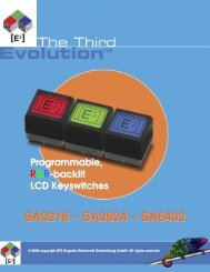
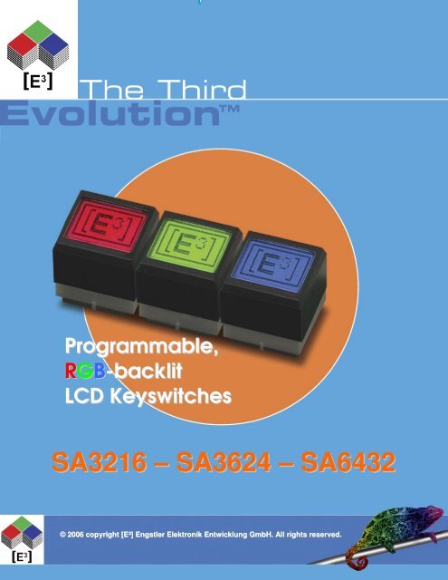
Programmable,<br />
RGB-backlit<br />
LCD Keyswitches<br />
<strong>SA</strong>3216 – <strong>SA</strong>3624 – <strong>SA</strong>6432<br />
© 2006 copyright [E³] Engstler Elektronik Entwicklung GmbH. All rights reserved.<br />
<strong>SA</strong> <strong>Technical</strong> <strong>Datasheet</strong> <strong>v2.1</strong>.doc
<strong>SA</strong>3216 – <strong>SA</strong>3624 – <strong>SA</strong>6432<br />
<strong>Technical</strong> <strong>Datasheet</strong><br />
intentionally left blank<br />
<strong>SA</strong> <strong>Technical</strong> <strong>Datasheet</strong> <strong>v2.1</strong>.doc<br />
2 of 31
<strong>SA</strong>3216 – <strong>SA</strong>3624 – <strong>SA</strong>6432<br />
<strong>Technical</strong> <strong>Datasheet</strong><br />
Table of Content<br />
Table of Content .............................................................................................................................. 3<br />
General Description ......................................................................................................................... 5<br />
Innovative Product Features ............................................................................................................ 5<br />
Resolution .....................................................................................................................................5<br />
RGB Colors ...................................................................................................................................5<br />
Color Calibration............................................................................................................................5<br />
Self-Initialisation ............................................................................................................................5<br />
Legacy Mode .............................................................................................................................5<br />
Low Power Consumption...............................................................................................................5<br />
<strong>Technical</strong> Overview.......................................................................................................................... 6<br />
<strong>SA</strong>3216 – <strong>SA</strong>3624 – <strong>SA</strong>6432........................................................................................................... 7<br />
Dimensions ...................................................................................................................................7<br />
Keyswitch ......................................................................................................................................7<br />
Layout ...........................................................................................................................................8<br />
Drill Masks.....................................................................................................................................8<br />
Mounting Methods.........................................................................................................................9<br />
Liquid Crystal Display..................................................................................................................10<br />
Environmental Specifications.......................................................................................................11<br />
Electrical Specifications...............................................................................................................11<br />
Interfacing <strong>SA</strong>326 - <strong>SA</strong>3624 - <strong>SA</strong>6432........................................................................................... 12<br />
Contact Terminals .......................................................................................................................12<br />
Block Diagram.............................................................................................................................13<br />
Serial Protocols ...........................................................................................................................14<br />
Legacy Mode (<strong>SA</strong>3216 and <strong>SA</strong>3624 only!).......................................................................... 14<br />
Advanced Technology Mode ............................................................................................... 15<br />
Timing Diagram ...................................................................................................................... 15<br />
Command Set .............................................................................................................................17<br />
Synchronous Protocol............................................................................................................. 17<br />
Command and Data Formats.................................................................................................. 17<br />
Commands ............................................................................................................................. 18<br />
<strong>SA</strong> <strong>Technical</strong> <strong>Datasheet</strong> <strong>v2.1</strong>.doc<br />
3 of 31
<strong>SA</strong>3216 – <strong>SA</strong>3624 – <strong>SA</strong>6432<br />
<strong>Technical</strong> <strong>Datasheet</strong><br />
Command Examples............................................................................................................... 20<br />
Bit / Pixel Mapping .................................................................................................................. 22<br />
Color Table ............................................................................................................................. 25<br />
Controlling <strong>SA</strong> Switch Arrays ......................................................................................................... 26<br />
Order Information........................................................................................................................... 27<br />
Change History.............................................................................................................................. 28<br />
Notices........................................................................................................................................... 29<br />
Copyright Notice..........................................................................................................................29<br />
<strong>Technical</strong> Notices ........................................................................................................................29<br />
Life Support Applications.............................................................................................................29<br />
Flammability Ratings ...................................................................................................................29<br />
Warranty Disclaimer ....................................................................................................................30<br />
Contact Information........................................................................................................................ 31<br />
<strong>SA</strong> <strong>Technical</strong> <strong>Datasheet</strong> <strong>v2.1</strong>.doc<br />
4 of 31
<strong>SA</strong>3216 – <strong>SA</strong>3624 – <strong>SA</strong>6432<br />
<strong>Technical</strong> <strong>Datasheet</strong><br />
General Description<br />
The <strong>SA</strong> switch family includes the <strong>SA</strong>3216, <strong>SA</strong>3624 and <strong>SA</strong>6432 LCD Keyswitches with<br />
command driven serial interfaces. They integrate a graphical liquid crystal display with<br />
RGB backlighting in a keyswitch. The <strong>SA</strong> keys are controlled via a serial interface to the<br />
integrated Advanced Technology electronics, which control the interface, display and<br />
backlighting. <strong>SA</strong> keys self-initialise without external setup commands. Data is only needs to<br />
be transmitted when a change is made to the display or background colors. Only six<br />
contact terminals are needed to provide power, clock and data lines as well as switch<br />
contacts. The contact pins of the internal switch are isolated from the internal electronics.<br />
Innovative Product Features<br />
Resolution<br />
Three different resolutions available: <strong>SA</strong>3216 32x16 pixels<br />
<strong>SA</strong>3624 36x24 pixels<br />
<strong>SA</strong>6432 64x32 pixels<br />
RGB Colors<br />
<strong>SA</strong>3216, <strong>SA</strong>3624 and <strong>SA</strong>6432 keys support 64 RGB colors.<br />
Color Calibration<br />
No color sorting due to Advanced Technology electronics. The RGB backlighting of all<br />
keyswitches is calibrated for maximum uniformity.<br />
Self-Initialisation<br />
All keys self-initialise. No external setup commands required.<br />
Legacy Mode<br />
Backward compatibility for use in legacy systems.<br />
Low Power Consumption<br />
Less than 60mA maximum current is needed when bright white backlighting is selected.<br />
Typical value is less than 25mA with one of the RGB colors.<br />
<strong>SA</strong> <strong>Technical</strong> <strong>Datasheet</strong> <strong>v2.1</strong>.doc<br />
5 of 31
<strong>SA</strong>3216 – <strong>SA</strong>3624 – <strong>SA</strong>6432<br />
<strong>Technical</strong> <strong>Datasheet</strong><br />
<strong>Technical</strong> Overview<br />
Features <strong>SA</strong>3216 <strong>SA</strong>3624 <strong>SA</strong>6432<br />
Resolution 32 x 16 36 x 24 64 x 32<br />
RGB backlight colors<br />
Interfaces<br />
Over 10,000 RGB colors<br />
Synchronous serial<br />
8-bit interfaces<br />
(custom protocols available upon request)<br />
Legacy Mode<br />
Synchronous serial<br />
12-bit interface<br />
External clock<br />
Extended<br />
Environmental<br />
Specifications<br />
Self-initialisation<br />
Required;<br />
60 kHz up to 2 MHz<br />
Upon request<br />
Yes<br />
No external clock<br />
required<br />
Hardened MIL-<br />
Spec version<br />
available<br />
(requires custom control<br />
panel development)<br />
Maximum speed<br />
Operating supply<br />
Keyswitch type<br />
Keyswitch life time<br />
Contact resistance<br />
Operating<br />
temperature<br />
2 MBaud<br />
4.9 V to 5.1 V<br />
tactile, 2.0 mm travel<br />
with over travel protection<br />
> 3.0 million cycles<br />
< 200 Ohm<br />
0°C to 55°C<br />
Storage temperature -30°C to 70°C<br />
<strong>SA</strong> <strong>Technical</strong> <strong>Datasheet</strong> <strong>v2.1</strong>.doc<br />
6 of 31
<strong>SA</strong>3216 – <strong>SA</strong>3624 – <strong>SA</strong>6432<br />
<strong>Technical</strong> <strong>Datasheet</strong><br />
<strong>SA</strong>3216 – <strong>SA</strong>3624 – <strong>SA</strong>6432<br />
Dimensions<br />
Dimensions ( X x Y x Z ) 24.5 x 23.5 x 26.0 mm + / - 0,2 mm<br />
Screen size ( X x Y )<br />
20.0 x 16.5 mm + / - 0.1 mm<br />
Keyswitch<br />
Key stroke<br />
Operation force:<br />
Over travel protection:<br />
Lifetime:<br />
2.0 mm +/- 0.1 mm; tactile<br />
1.3 N +/- 0.2 N<br />
yes<br />
> 3 million cycles<br />
Tactile Force Curve<br />
<strong>SA</strong> <strong>Technical</strong> <strong>Datasheet</strong> <strong>v2.1</strong>.doc<br />
7 of 31
<strong>SA</strong>3216 – <strong>SA</strong>3624 – <strong>SA</strong>6432<br />
<strong>Technical</strong> <strong>Datasheet</strong><br />
Layout<br />
Direct PCB Mount<br />
(top view)<br />
Socket Mount<br />
(top view)<br />
Drill Masks<br />
for direct soldering<br />
(top view)<br />
for use with socket pins<br />
(top view)<br />
<strong>SA</strong> <strong>Technical</strong> <strong>Datasheet</strong> <strong>v2.1</strong>.doc<br />
8 of 31
<strong>SA</strong>3216 – <strong>SA</strong>3624 – <strong>SA</strong>6432<br />
<strong>Technical</strong> <strong>Datasheet</strong><br />
Recommended distance for array assembly is 1mm between each key.<br />
Mounting Methods<br />
Socket mountable (see corresponding Drill Mask). Socket pins (SP0000) and socket locks<br />
(SL0000) are used for field-exchangeable mounting.<br />
Through-hole mountable on PCBs with x, y, z mm thickness<br />
Manual soldering: max. 350° C for max. 3.5 seconds per pin<br />
Wave soldering:<br />
260° C for 10 seconds<br />
<strong>SA</strong> <strong>Technical</strong> <strong>Datasheet</strong> <strong>v2.1</strong>.doc<br />
9 of 31
<strong>SA</strong>3216 – <strong>SA</strong>3624 – <strong>SA</strong>6432<br />
<strong>Technical</strong> <strong>Datasheet</strong><br />
Liquid Crystal Display<br />
Screen Size (X x Y)<br />
17.26 mm x 12.14 mm<br />
Pixel Size (X x Y) <strong>SA</strong>3216 0.52 mm x 0.74 mm<br />
<strong>SA</strong>3624 0.46 mm x 0.48 mm<br />
<strong>SA</strong>6432 0.25 mm x 0.36 mm<br />
<strong>SA</strong> <strong>Technical</strong> <strong>Datasheet</strong> <strong>v2.1</strong>.doc<br />
10 of 31
<strong>SA</strong>3216 – <strong>SA</strong>3624 – <strong>SA</strong>6432<br />
<strong>Technical</strong> <strong>Datasheet</strong><br />
Environmental Specifications<br />
Operating temperature 0°C to 55°C<br />
Storage temperature -30°C to 70°C<br />
Humidity up to 75% relative humidity at 70°C<br />
Electrical Specifications<br />
Operating voltage<br />
Current consumption<br />
Contact resistance<br />
Insulating resistance<br />
4.9 V to 5.1 V<br />
max. 60 mA; typ. < 30 mA; min. 8 mA<br />
< 200 Ohm<br />
> 100 MOhm<br />
Symbol Parameter Min. Typ. Max. Unit<br />
V DD * 1) Operating voltage 4.9 5.1 V<br />
I DD * 2) Supply current 8
<strong>SA</strong>3216 – <strong>SA</strong>3624 – <strong>SA</strong>6432<br />
<strong>Technical</strong> <strong>Datasheet</strong><br />
Interfacing <strong>SA</strong>326 - <strong>SA</strong>3624 - <strong>SA</strong>6432<br />
Contact Terminals<br />
Pin Symbol Description<br />
Comment<br />
1 GND negative (ground) power terminal 0.0 V<br />
2 + 5V positive power terminal +4.9 V – +5.1 V<br />
3 CLOCK<br />
4 DATA<br />
clock line to synchronize data write and for<br />
internal use<br />
command and data line to internal Advanced<br />
Technology electronics<br />
60 kHz – 2 MHz<br />
HIGH when inactive;<br />
see data format for details<br />
5 SW1 switch contact<br />
6 SW2 switch contact<br />
contact resistance<br />
< 200 Ohm<br />
contact resistance<br />
< 200 Ohm<br />
Pin View (terminal name and number are also marked on the keyswitch)<br />
<strong>SA</strong> <strong>Technical</strong> <strong>Datasheet</strong> <strong>v2.1</strong>.doc<br />
12 of 31
<strong>SA</strong>3216 – <strong>SA</strong>3624 – <strong>SA</strong>6432<br />
<strong>Technical</strong> <strong>Datasheet</strong><br />
Block Diagram<br />
<strong>SA</strong> <strong>Technical</strong> <strong>Datasheet</strong> <strong>v2.1</strong>.doc<br />
13 of 31
<strong>SA</strong>3216 – <strong>SA</strong>3624 – <strong>SA</strong>6432<br />
<strong>Technical</strong> <strong>Datasheet</strong><br />
Serial Protocols<br />
The <strong>SA</strong>3216, <strong>SA</strong>3624 and <strong>SA</strong>6432 keyswitches are connected to the controlling central<br />
processing unit by a 2 wire serial connection.<br />
Currently, the <strong>SA</strong> switches support two different protocols:<br />
Legacy Mode (<strong>SA</strong>3216 and <strong>SA</strong>3624 only!)<br />
Advanced Technology Mode<br />
Additional protocols are available upon request. Please contact your local [E³]<br />
distributor or [E³] directly at techsupport@e3-keys.com.<br />
Feature<br />
Legacy<br />
Mode<br />
Advanced<br />
Technology<br />
Mode<br />
Clock Frequency 64 kHz to 2 MHz up to 2 MHz<br />
Permanent Clock Yes No<br />
Data Word Size 12 bit 8 bit<br />
Internal Serial Number No Yes*<br />
Internal Failure Detection No Yes*<br />
* To take advantage of these advanced functions your hardware must ensure<br />
that the <strong>SA</strong> keys are actively driving the serial data lines in Advanced<br />
Technology mode.<br />
LEGACY MODE (<strong>SA</strong>3216 AND <strong>SA</strong>3624 ONLY!)<br />
Legacy Mode applies only to the use of <strong>SA</strong>3216 and <strong>SA</strong>3624 keyswitches in legacy<br />
systems. This mode is supported in order to ease the transition to the new possibilities of<br />
the <strong>SA</strong> switches in existing hardware environments. The intelligent electronics of the <strong>SA</strong><br />
switches detect the existing protocol and automatically convert the data into the data<br />
stream that is required for <strong>SA</strong> switches. In order to make a system compatible with the<br />
Legacy Mode it may be necessary to adjust the clock frequency and/or to increase the<br />
transfer bit count per data word.<br />
If you have questions regarding the implementation of Legacy Mode, please contact<br />
your local [E³] distributor or [E³]’s R&D department directly at techsupport@e3-keys.com.<br />
<strong>SA</strong> <strong>Technical</strong> <strong>Datasheet</strong> <strong>v2.1</strong>.doc<br />
14 of 31
<strong>SA</strong>3216 – <strong>SA</strong>3624 – <strong>SA</strong>6432<br />
<strong>Technical</strong> <strong>Datasheet</strong><br />
ADVANCED TECHNOLOGY MODE<br />
This is the standard mode for controlling <strong>SA</strong> keyswitches and provides full access to all<br />
capabilities of the <strong>SA</strong>3216, <strong>SA</strong>3624 and <strong>SA</strong>6432 keys. The details of this control protocol<br />
are documented in the subsequent paragraphs<br />
The Advanced Technology Mode uses a conventional synchronous protocol. A<br />
permanently applied clock is not necessary.<br />
The only difference to a true 8-bit synchronous data transmission is that the data may also<br />
be synchronized to a permanently applied clock. No parity checking/generation is required.<br />
Since it is possible that the clock is applied permanently a StartBit is required to be able to<br />
detect the start of a transmission. To allow for a StartBit in a standard synchronous SPI the<br />
MSB of the DataByte is to be set to 0.<br />
Note: Customer-specific protocols are possible. Future versions will include other types of<br />
interfaces such as I²C bus and asynchronous protocols<br />
TIMING DIAGRAM<br />
Note: Clock and Data lines must be set to HIGH when inactive.<br />
<strong>SA</strong> <strong>Technical</strong> <strong>Datasheet</strong> <strong>v2.1</strong>.doc<br />
15 of 31
<strong>SA</strong>3216 – <strong>SA</strong>3624 – <strong>SA</strong>6432<br />
<strong>Technical</strong> <strong>Datasheet</strong><br />
Symbol Parameter Min Max Unit<br />
t c (CLK) SPI Clock frequency 0.06 2 MHz<br />
t w (CLKH) Clock high time 90 ns<br />
tw(CLKL) Clock low time 90 ns<br />
t su (D) Data input setup time 140 ns<br />
t h (D) Data input hold time 100 ns<br />
t r (CLK) Clock rise time 15 ns<br />
t f (CLK) Clock fall time 15 ns<br />
Note: In order to ensure proper<br />
synchronization to the data, if there<br />
is a permanently applied clock, the<br />
command and data bytes should<br />
follow each other either without a<br />
gap or with a gap of more than 8<br />
clock cycles.<br />
The time between data bytes may<br />
not exceed 1ms or the protocol will<br />
terminate current command.<br />
<strong>SA</strong> <strong>Technical</strong> <strong>Datasheet</strong> <strong>v2.1</strong>.doc<br />
16 of 31
<strong>SA</strong>3216 – <strong>SA</strong>3624 – <strong>SA</strong>6432<br />
<strong>Technical</strong> <strong>Datasheet</strong><br />
Command Set<br />
SYNCHRONOUS PROTOCOL<br />
The command structure is quite simple as you can see in the following table. Due to the<br />
possibility of a permanently applied clock each transmitted data must have a leading “0”. To<br />
distinguish between command and data the sixth bit is reserved. There are three sets of<br />
commands:<br />
Write Data to the LCD Display<br />
Set Backlight Color<br />
Extended Command Set<br />
The first two command sets imply the required data and do not expect a return value from<br />
the key. Some commands in the Extended Command set, however, request information to<br />
be returned by the key. In this case, the Advanced Technology electronics will generate<br />
their own clock signal for the data transmission. For details on this scenario, see the<br />
Applications Notes on our website www.e3-keys.com.<br />
Note:If you are running the keys in a Legacy Mode environment you cannot use the<br />
extended commands since legacy systems do not support returning information from the<br />
keys. This may cause a hardware collision, which may result in damage to your system.<br />
COMMAND AND DATA FORMATS<br />
Command<br />
(binary<br />
representation)<br />
01xxxxxx<br />
Command Name /<br />
Description<br />
Command format<br />
Comments<br />
“xxxxxx” contains command values according to<br />
the Commands table on page 15.<br />
00xxxxxx Data format Data to be sent to the key must always have bit 6<br />
reset.<br />
Note: All commands and data will have bit 7<br />
reset in order to make the protocol compatible<br />
with systems having a permanently applied<br />
clock.<br />
<strong>SA</strong> <strong>Technical</strong> <strong>Datasheet</strong> <strong>v2.1</strong>.doc<br />
17 of 31
<strong>SA</strong>3216 – <strong>SA</strong>3624 – <strong>SA</strong>6432<br />
<strong>Technical</strong> <strong>Datasheet</strong><br />
COMMANDS<br />
Command<br />
(binary<br />
representation)<br />
Command Name /<br />
Description<br />
Comments<br />
All writes to the display must be initiated by this<br />
command. Address pointer is auto-incremented by<br />
data transmission.<br />
The command expects min. 4 data words to follow:<br />
01000000<br />
(0x40)<br />
01000001<br />
(0x41)<br />
01000010<br />
(0x42)<br />
01000011<br />
(0x43)<br />
Set Display Address &<br />
Write Display Data<br />
Set Color<br />
Set RGB Color<br />
End Transmission<br />
0000000A 8<br />
0000A 7 A 6 A 5 A 4<br />
0000A 3 A 2 A 1 A 0<br />
0000D 3 D 2 D 1 D 0<br />
Multiple Data Bytes may follow without<br />
additional addressing in one sequence since<br />
the controller will perform auto-increment<br />
Details are found in the Bit/Pixel Mapping tables<br />
on pages 18-20.<br />
There is one data word to follow:<br />
00R 1 R 0 G 1 G 0 B 1 B 0<br />
Details are found in the Color table on page 21.<br />
There are 3 data bytes to follow:<br />
0D 6 D 5 D 4 D 3 D 2 D 1 D 0<br />
0D 6 D 5 D 4 D 3 D 2 D 1 D 0<br />
0D 6 D 5 D 4 D 3 D 2 D 1 D 0<br />
Note: The lower 10 values on each color<br />
brightness value should only be used for<br />
single color applications due to restrictions<br />
in the color calibration.<br />
These colors may change and should be used with<br />
caution until otherwise noted by [E³]<br />
Ends data transmission to keys and awaits next<br />
command sequence. Transmitted commands are<br />
begin processed and displayed.<br />
This command should be placed at the end of a<br />
sequence.<br />
<strong>SA</strong> <strong>Technical</strong> <strong>Datasheet</strong> <strong>v2.1</strong>.doc<br />
18 of 31
<strong>SA</strong>3216 – <strong>SA</strong>3624 – <strong>SA</strong>6432<br />
<strong>Technical</strong> <strong>Datasheet</strong><br />
01000100<br />
(0x44)<br />
01000101<br />
(0x45)<br />
Read Keyswitch ID<br />
THIS COMMAND<br />
FORCES THE<br />
KEYSWITCH TO<br />
ANSWER ON THE<br />
CLOCK AND DATA<br />
LINE.<br />
(The clock is generated by the<br />
<strong>SA</strong> switch; see Application<br />
Notes at www.e3-keys.com)<br />
Read Serial Number<br />
THIS COMMAND<br />
FORCES THE<br />
KEYSWITCH TO<br />
ANSWER ON THE<br />
CLOCK AND DATA<br />
LINE.<br />
(The clock is generated by the<br />
<strong>SA</strong> switch; see Application<br />
Notes at www.e3-keys.com)<br />
The answer is consisting of ASCII characters<br />
representing the Keyswitch ID and is terminated<br />
with CR (0x0D):<br />
<strong>SA</strong>3216<br />
<strong>SA</strong>3624<br />
<strong>SA</strong>6432<br />
(not supported in Legacy Mode)<br />
The answer is consisting of 4 Bytes which give the<br />
serial Number in the following format and is<br />
terminated with CR (0x0D):<br />
SNYYWW#####<br />
Year (04-99)<br />
Week (01-52)<br />
Number (00000 .. 99999)<br />
(not supported in Legacy Mode)<br />
<strong>SA</strong> <strong>Technical</strong> <strong>Datasheet</strong> <strong>v2.1</strong>.doc<br />
19 of 31
<strong>SA</strong>3216 – <strong>SA</strong>3624 – <strong>SA</strong>6432<br />
<strong>Technical</strong> <strong>Datasheet</strong><br />
COMMAND EXAMPLES<br />
Set display address to point to upper right corner of display:<br />
01000000 00000000 00000000 0000000 (0x40 0x00 0x00 0x00)<br />
Write Data to Display<br />
Binary HEX Comments<br />
01000000 0x40 Set display address & Write to Display<br />
00000000 0x00 Data: 00000 for A 8<br />
00000000 0x00 Data: 00000 for A 7 A 6 A 5 A 4<br />
00000000 0x00 Data: 00000 for A 3 A 2 A 1 A 0<br />
00000101 0x05 Write pattern 0101 to LCD Display and increment address by 1<br />
00000101 0x05 Write pattern 0101 to LCD Display and increment address by 1<br />
00000101 0x05 Write pattern 0101 to LCD Display and increment address by 1<br />
00000101 0x05 Write pattern 0101 to LCD Display and increment address by 1<br />
Set backlighting color to light orange:<br />
01000001 00111000 ( 0x41 0x38)<br />
Binary HEX Comments<br />
01000001 0x41 Set color<br />
00111000 0x38 Red: high intensity, Green medium intensity, Blue off<br />
The 2 individual bits for each color intensity have the following structure:<br />
00 = off<br />
01 = low<br />
10 = medium<br />
11 = high<br />
End transmission and process data:<br />
01000011 (0x43)<br />
Binary HEX Comments<br />
01000011 0x43 End transmission<br />
<strong>SA</strong> <strong>Technical</strong> <strong>Datasheet</strong> <strong>v2.1</strong>.doc<br />
20 of 31
<strong>SA</strong>3216 – <strong>SA</strong>3624 – <strong>SA</strong>6432<br />
<strong>Technical</strong> <strong>Datasheet</strong><br />
Read Keyswitch ID:<br />
01001000 (0x48)<br />
Binary HEX Comments<br />
01001000 0x48 Read Keyswitch ID<br />
The Key will answer by generating its own clock and data signals (see Application Notes at<br />
www.e3-keys.com for details)<br />
The following examples show the answers for the different <strong>SA</strong>xxxx types:<br />
0x53 0x41 0x33 0x32 0x31 0x36 0x0D = <strong>SA</strong>3216 CR<br />
0x53 0x41 0x33 0x36 0x32 0x34 0x0D = <strong>SA</strong>3624 CR<br />
0x53 0x41 0x36 0x34 0x33 0x32 0x0D = <strong>SA</strong>6432 CR<br />
Read Serial Number:<br />
01001001 (0x49)<br />
Binary HEX Comments<br />
01001001 0x49 Read Serial Number (SNYYWW#####)<br />
The Key will answer by generating its own clock and data signals (see Application Notes at<br />
www.e3-keys.com for details)<br />
The following example shows the format of the answer:<br />
0x53 0x4E 0x30 0x34 0x30 0x33 0x30 0x35 0x30 0x39 0x33 0x0D = SN040305093CR<br />
<strong>SA</strong> <strong>Technical</strong> <strong>Datasheet</strong> <strong>v2.1</strong>.doc<br />
21 of 31
<strong>SA</strong>3216 – <strong>SA</strong>3624 – <strong>SA</strong>6432<br />
<strong>Technical</strong> <strong>Datasheet</strong><br />
BIT / PIXEL MAPPING<br />
Display Memory – Internal RAM Structure<br />
The static display RAM holds the data for the LCD display. This data is displayed<br />
automatically and is continuously refreshed without further interference from the host<br />
controller.<br />
The display RAM is organized into 512 x 4 bits and stores the display data in the <strong>SA</strong> switch.<br />
The content of the display RAM is mapped directly to the LCD display. This RAM can be<br />
accessed by the Write LCD Data command, which must be preceded by the Set LCD<br />
Address command. The SET LCD Address command tells the key where to write the data<br />
and where to display it on the LCD. For actual RAM-Display mapping please refer to the<br />
corresponding Bit/Pixel mapping tables below.<br />
Bit/Pixel Mapping Table for <strong>SA</strong>3216<br />
Column 31<br />
Column 30<br />
Column 29<br />
Column 28<br />
…<br />
Column 3<br />
Column 2<br />
Column 1<br />
Column 0<br />
Address 7CH 78H 74H 70H … 0CH 08H 04H 00H<br />
Row 0 D 0 D 0 D 0 D 0 … D 0 D 0 D 0 D 0<br />
Row 1 D 1 D 1 D 1 D 1 … D 1 D 1 D 1 D 1<br />
Row 2 D 2 D 2 D 2 D 2 … D 2 D 2 D 2 D 2<br />
Row 3 D 3 D 3 D 3 D 3 … D 3 D 3 D 3 D 3<br />
Address 7DH 79H 75H 71H … 0DH 09H 05H 01H<br />
Row 4 D 0 D 0 D 0 D 0 … D 0 D 0 D 0 D 0<br />
Row 5 D 1 D 1 D 1 D 1 … D 1 D 1 D 1 D 1<br />
Note:<br />
The display can also be<br />
inscribed by using 0x0f<br />
as data in the not<br />
available positions.<br />
Example:<br />
0x40 0x00 0x00<br />
0x00 0xyy 0xzz<br />
0xaa 0xbb 0x0f<br />
0x0f 0xcc 0xdd<br />
0xee 0xff<br />
Row 6 D 2 D 2 D 2 D 2 … D 2 D 2 D 2 D 2<br />
Row 7 D 3 D 3 D 3 D 3 … D 3 D 3 D 3 D 3<br />
Address 7EH 7AH 76H 72H … 0EH 0AH 06H 02H<br />
Row 8 D 0 D 0 D 0 D 0 … D 0 D 0 D 0 D 0<br />
Row 9 D 1 D 1 D 1 D 1 … D 1 D 1 D 1 D 1<br />
Row 10 D 2 D 2 D 2 D 2 … D 2 D 2 D 2 D 2<br />
Row 11 D 3 D 3 D 3 D 3 … D 3 D 3 D 3 D 3<br />
Address 7FH 7BH 77H 73H … 0FH 0BH 07H 03H<br />
Row 12 D 0 D 0 D 0 D 0 … D 0 D 0 D 0 D 0<br />
Row 13 D 1 D 1 D 1 D 1 … D 1 D 1 D 1 D 1<br />
This has the same<br />
result as<br />
0x40 0x00 0x00<br />
0x00 0xyy 0xzz<br />
0xaa 0xbb 0x40<br />
0x00 0x00 0x06<br />
0xcc 0xdd 0xee<br />
0xff<br />
Row 14 D 2 D 2 D 2 D 2 … D 2 D 2 D 2 D 2<br />
Row 15 D 3 D 3 D 3 D 3 … D 3 D 3 D 3 D 3<br />
<strong>SA</strong> <strong>Technical</strong> <strong>Datasheet</strong> <strong>v2.1</strong>.doc<br />
22 of 31
<strong>SA</strong>3216 – <strong>SA</strong>3624 – <strong>SA</strong>6432<br />
<strong>Technical</strong> <strong>Datasheet</strong><br />
Bit/Pixel Mapping Table for <strong>SA</strong>3624<br />
Column 35<br />
Column 34<br />
Column 33<br />
Address 11EH 116H 10EH … 1EH 16H 0EH 06H<br />
Row 16 D 0 D 0 D 0 … D 0 D 0 D 0 D 0<br />
Row 17 D 1 D 1 D 1 … D 1 D 1 D 1 D 1<br />
Row 18 D 2 D 2 D 2 … D 2 D 2 D 2 D 2<br />
Row 19 D 3 D 3 D 3 … D 3 D 3 D 3 D 3<br />
Address 11FH 117H 10FH … 1FH 17H 0FH 07H<br />
Row 20 D 0 D 0 D 0 … D 0 D 0 D 0 D 0<br />
Row 21 D 1 D 1 D 1 … D 1 D 1 D 1 D 1<br />
Row 22 D 2 D 2 D 2 … D 2 D 2 D 2 D 2<br />
Row 23 D 3 D 3 D 3 … D 3 D 3 D 3 D 3<br />
Address 118H 110H 108H ... 18H 10H 08H 00H<br />
Row 0 D 0 D 0 D 0 ... D 0 D 0 D 0 D 0<br />
Row 1 D 1 D 1 D 1 … D 1 D 1 D 1 D 1<br />
Row 2 D 2 D 2 D 2 … D 2 D 2 D 2 D 2<br />
Row 3 D 3 D 3 D 3 … D 3 D 3 D 3 D 3<br />
Address 119H 111H 109H … 19H 11H 09H 01H<br />
Row 4 D 0 D 0 D 0 … D 0 D 0 D 0 D 0<br />
Row 5 D 1 D 1 D 1 … D 1 D 1 D 1 D 1<br />
Row 6 D 2 D 2 D 2 … D 2 D 2 D 2 D 2<br />
Row 7 D 3 D 3 D 3 … D 3 D 3 D 3 D 3<br />
Address 11AH 112H 10AH … 1AH 12H 0AH 02H<br />
Row 8 D 0 D 0 D 0 … D 0 D 0 D 0 D 0<br />
Row 9 D 1 D 1 D 1 … D 1 D 1 D 1 D 1<br />
Row 10 D 2 D 2 D 2 … D 2 D 2 D 2 D 2<br />
Row 11 D 3 D 3 D 3 … D 3 D 3 D 3 D 3<br />
Address 11BH 113H 10BH … 1BH 13H 0BH 03H<br />
Row 12 D 0 D 0 D 0 … D 0 D 0 D 0 D 0<br />
Row 13 D 1 D 1 D 1 … D 1 D 1 D 1 D 1<br />
Row 14 D 2 D 2 D 2 … D 2 D 2 D 2 D 2<br />
Row 15 D 3 D 3 D 3 … D 3 D 3 D 3 D 3<br />
…<br />
Column 3<br />
Column 2<br />
Column 1<br />
Column 0<br />
<strong>SA</strong> <strong>Technical</strong> <strong>Datasheet</strong> <strong>v2.1</strong>.doc<br />
23 of 31
<strong>SA</strong>3216 – <strong>SA</strong>3624 – <strong>SA</strong>6432<br />
<strong>Technical</strong> <strong>Datasheet</strong><br />
Bit/Pixel Mapping Table for <strong>SA</strong>6432<br />
Column 63<br />
Column 62<br />
Column 61<br />
Column 60<br />
…<br />
Column 3<br />
Column 2<br />
Column 1<br />
Column 0<br />
Address 1FCH 1F4H 1ECH 1E4H … 1CH 14H 0CH 04H<br />
Row 16 D 0 D 0 D 0 D 0 … D 0 D 0 D 0 D 0<br />
Row 17 D 1 D 1 D 1 D 1 … D 1 D 1 D 1 D 1<br />
Row 18 D 2 D 2 D 2 D 2 … D 2 D 2 D 2 D 2<br />
Row 19 D 3 D 3 D 3 D 3 … D 3 D 3 D 3 D 3<br />
Address 1FDH 1F5H 1EDH 1E5H … 1DH 15H 0DH 05H<br />
Row 20 D 0 D 0 D 0 D 0 … D 0 D 0 D 0 D 0<br />
Row 21 D 1 D 1 D 1 D 1 … D 1 D 1 D 1 D 1<br />
Row 22 D 2 D 2 D 2 D 2 … D 2 D 2 D 2 D 2<br />
Row 23 D 3 D 3 D 3 D 3 … D 3 D 3 D 3 D 3<br />
Address 1FEH 1F6H 1EEH 1E6H … 1EH 16H 0EH 06H<br />
Row 24 D 0 D 0 D 0 D 0 … D 0 D 0 D 0 D 0<br />
Row 25 D 1 D 1 D 1 D 1 … D 1 D 1 D 1 D 1<br />
Row 26 D 2 D 2 D 2 D 2 … D 2 D 2 D 2 D 2<br />
Row 27 D 3 D 3 D 3 D 3 … D 3 D 3 D 3 D 3<br />
Address 1FFH 1F7H 1EFH 1E7H … 1FH 17H 0FH 07H<br />
Row 28 D 0 D 0 D 0 D 0 … D 0 D 0 D 0 D 0<br />
Row 29 D 1 D 1 D 1 D 1 … D 1 D 1 D 1 D 1<br />
Row 30 D 2 D 2 D 2 D 2 … D 2 D 2 D 2 D 2<br />
Row 31 D 3 D 3 D 3 D 3 … D 3 D 3 D 3 D 3<br />
Address 1F8H 1F0H 1E8H 1E0H ... 18H 10H 08H 00H<br />
Row 0 D 0 D 0 D 0 D 0 ... D 0 D 0 D 0 D 0<br />
Row 1 D 1 D 1 D 1 D 1 … D 1 D 1 D 1 D 1<br />
Row 2 D 2 D 2 D 2 D 2 … D 2 D 2 D 2 D 2<br />
Row 3 D 3 D 3 D 3 D 3 … D 3 D 3 D 3 D 3<br />
Address 1F9H 1F1H 1E9H 1E1H … 19H 11H 09H 01H<br />
Row 4 D 0 D 0 D 0 D 0 … D 0 D 0 D 0 D 0<br />
Row 5 D 1 D 1 D 1 D 1 … D 1 D 1 D 1 D 1<br />
Row 6 D 2 D 2 D 2 D 2 … D 2 D 2 D 2 D 2<br />
Row 7 D 3 D 3 D 3 D 3 … D 3 D 3 D 3 D 3<br />
Address 1FAH 1F2H 1EAH 1E2H … 1AH 12H 0AH 02H<br />
Row 8 D 0 D 0 D 0 D 0 … D 0 D 0 D 0 D 0<br />
Row 9 D 1 D 1 D 1 D 1 … D 1 D 1 D 1 D 1<br />
Row 10 D 2 D 2 D 2 D 2 … D 2 D 2 D 2 D 2<br />
Row 11 D 3 D 3 D 3 D 3 … D 3 D 3 D 3 D 3<br />
Address 1FBH 1F3H 1EBH 1E3H … 1BH 13H 0BH 03H<br />
Row 12 D 0 D 0 D 0 D 0 … D 0 D 0 D 0 D 0<br />
Row 13 D 1 D 1 D 1 D 1 … D 1 D 1 D 1 D 1<br />
Row 14 D 2 D 2 D 2 D 2 … D 2 D 2 D 2 D 2<br />
Row 15 D 3 D 3 D 3 D 3 … D 3 D 3 D 3 D 3<br />
<strong>SA</strong> <strong>Technical</strong> <strong>Datasheet</strong> <strong>v2.1</strong>.doc<br />
24 of 31
<strong>SA</strong>3216 – <strong>SA</strong>3624 – <strong>SA</strong>6432<br />
<strong>Technical</strong> <strong>Datasheet</strong><br />
COLOR TABLE<br />
The color command 01000001 (0x41) initiates the color settings of the <strong>SA</strong> keyswitches with<br />
two bits for the color intensity setting of each color.<br />
The color approximations for <strong>SA</strong>3216, <strong>SA</strong>3624 & <strong>SA</strong>6432 keys are shown in following color<br />
table. This table is intended for illustration purposes only. The actual display colors on the<br />
LCD display with LED backlighting may be different.<br />
<strong>SA</strong> <strong>Technical</strong> <strong>Datasheet</strong> <strong>v2.1</strong>.doc<br />
25 of 31
<strong>SA</strong>3216 – <strong>SA</strong>3624 – <strong>SA</strong>6432<br />
<strong>Technical</strong> <strong>Datasheet</strong><br />
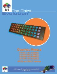
Controlling <strong>SA</strong> Switch Arrays<br />
Below are sample schematics for controlling one or sixteen <strong>SA</strong> keyswitches in an array<br />
using a PIC16F62X controller to illustrate the simplicity of the control circuitry. Further<br />
descriptions including sources are available under the Application Notes at our website at<br />
www.e3-keys.com.<br />
For additional technical support with your own design implementation, please contact your<br />
local [E³] distributor or [E³] at techsupport@e3-keys.com.<br />
In the above examples the clock and data signals are generated on the corresponding I/O<br />
pins of the PIC controller.<br />
<strong>SA</strong> <strong>Technical</strong> <strong>Datasheet</strong> <strong>v2.1</strong>.doc<br />
26 of 31
<strong>SA</strong>3216 – <strong>SA</strong>3624 – <strong>SA</strong>6432<br />
<strong>Technical</strong> <strong>Datasheet</strong><br />
Order Information<br />
Part Number<br />
<strong>SA</strong>3216-B<br />
<strong>SA</strong>3624-B<br />
<strong>SA</strong>6432-B<br />
Description<br />
<strong>SA</strong> pushbutton keyswitch with 32x16 pixel display<br />
Backlit in 64 RGB colors<br />
Black housing (RAL 9005)<br />
<strong>SA</strong> pushbutton keyswitch with 36 x 24 pixel display<br />
Backlit in 64 RGB colors<br />
Black housing (RAL 9005)<br />
<strong>SA</strong> pushbutton keyswitch with 64 x 32 pixel display<br />
Backlit in 64 RGB colors<br />
Black housing (RAL 9005)<br />
SP0000<br />
Socket pin set for use with the <strong>SA</strong>xxxx switches<br />
DS0000<br />
DemoBoard for use with 2 <strong>SA</strong>xxxx keys with RS232 interface<br />
Keys are not included.<br />
Full documentation and software available at www.e3-keys.com.<br />
Other housing colors available on request<br />
<strong>SA</strong> <strong>Technical</strong> <strong>Datasheet</strong> <strong>v2.1</strong>.doc<br />
27 of 31
<strong>SA</strong>3216 – <strong>SA</strong>3624 – <strong>SA</strong>6432<br />
<strong>Technical</strong> <strong>Datasheet</strong><br />
Change History<br />
Version Date Comments<br />
0.1 10/06/03 Initial draft document<br />
0.2 11/13/03 Updated draft document<br />
0.3 11/14/03 Final draft document<br />
1.0 11/19/03 <strong>Technical</strong> <strong>Datasheet</strong> v1.0<br />
1.1 02/25/04<br />
1.2 04/07/04<br />
2.0 01/27/06<br />
Correction of typographical errors<br />
Tactile force curve illustration updated<br />
Layout illustration updated<br />
Supply voltage 4.9 to 5.1 V<br />
Bit/Pixel Mapping Table for <strong>SA</strong>6432 changed<br />
Bit/Pixel Mapping Table for <strong>SA</strong>3624 changed<br />
Clock phase corrected compatibility reasons to Legacy<br />
Legacy Mode and Advanced Technology Mode protocols<br />
updated<br />
Application Notes reference added<br />
Table page references added<br />
Change History added<br />
Clock rise and fall time corrected<br />
Page 21 color command is 0x41 not 0x42<br />
Comment to command 0x43 added<br />
<strong>Technical</strong> update v2.0<br />
Life support application notice added<br />
Flammability ratings added<br />
2.1 07/03/07 Reduced I/O data pin capacitance value changed<br />
<strong>SA</strong> <strong>Technical</strong> <strong>Datasheet</strong> <strong>v2.1</strong>.doc<br />
28 of 31
<strong>SA</strong>3216 – <strong>SA</strong>3624 – <strong>SA</strong>6432<br />
<strong>Technical</strong> <strong>Datasheet</strong><br />
Notices<br />
Copyright Notice<br />
© 2003-2006 Copyright [E³] Engstler Elektronik Entwicklung GmbH. All<br />
rights reserved.<br />
[E³], The Third Evolution and Legacy Mode are trademarks of [E³]. The<br />
Keys to Intelligence is a trademark of I/O Universal Technologies, Inc.<br />
used with permission. All other trademarks are property of their<br />
respective owners.<br />
No part of this publication may be copied, photocopied, reproduced,<br />
translated or reduced to any electronic medium or machine-readable form<br />
without the expressed written consent of [E³] Engstler Elektronik<br />
Entwicklung GmbH.<br />
<strong>Technical</strong> Notices<br />
This datasheet is intended for technically qualified personnel trained in<br />
the field of electronics.<br />
The knowledge of electronics and the technically correct implementation<br />
of the content of this datasheet are required for problem free<br />
installation, implementation and safe operation of the described product.<br />
Only qualified personnel have the required know-how to implement the<br />
specifications given in this data sheet.<br />
For clarity, not all details regarding the product or its implementation,<br />
installation, operation, or maintenance have been included. Should you<br />
require additional information or further assistance, please contact your<br />
local [E³] distributor or [E³] Engstler Elektronik Entwicklung GmbH at<br />
techsupport@e3-keys.com. You may also visit our website at www.e3-keys.com.<br />
Life Support Applications<br />
The products discussed in this document are not designed for use in life<br />
support appliances, devices, or systems where malfunction of these<br />
products can reasonably be expected to result in personal injury. [E³]<br />
customers using or selling these products for use in such applications do<br />
so at their own risk and agree to fully indemnify [E³] for any damages<br />
resulting from such improper use or sale.<br />
Flammability Ratings<br />
The <strong>SA</strong>xxxx base is rated UL94-V0; all other plastics are rated UL94-HB.<br />
<strong>SA</strong> <strong>Technical</strong> <strong>Datasheet</strong> <strong>v2.1</strong>.doc<br />
29 of 31
<strong>SA</strong>3216 – <strong>SA</strong>3624 – <strong>SA</strong>6432<br />
<strong>Technical</strong> <strong>Datasheet</strong><br />
Warranty Disclaimer<br />
[E³] ENGSTLER ELEKTRONIK ENTWICKLUNG GMBH grants no warranty with respect<br />
to this data sheet, neither explicit nor implied, and it is not liable<br />
for direct or indirect damages. Some states do not grant the exclusion of<br />
incidental or consequential damages and, therefore, this statement may<br />
not be valid in such cases.<br />
This data sheet has been produced with all due care. However, since<br />
errors cannot be excluded, [E³] Engstler Elektronik Entwicklung GmbH does<br />
not grant any warranty or accept any legal responsibility or liability in<br />
any form for erroneous statements herein.<br />
<strong>SA</strong> <strong>Technical</strong> <strong>Datasheet</strong> <strong>v2.1</strong>.doc<br />
30 of 31
<strong>SA</strong>3216 – <strong>SA</strong>3624 – <strong>SA</strong>6432<br />
<strong>Technical</strong> <strong>Datasheet</strong><br />
Contact Information<br />
[E³]<br />
Engstler<br />
Elektronik<br />
Entwicklung<br />
GmbH<br />
Industriering 7<br />
63868 Grosswallstadt<br />
Germany<br />
Phone: +49 (0) 6022 262570<br />
Fax: +49 (0) 6022 262571<br />
E-Mail: info@e3-keys.com<br />
<strong>SA</strong> <strong>Technical</strong> <strong>Datasheet</strong> <strong>v2.1</strong>.doc<br />
31 of 31