Increase Bandwidth for Circular Microstrip Patch Antenna
Increase Bandwidth for Circular Microstrip Patch Antenna
Increase Bandwidth for Circular Microstrip Patch Antenna

You also want an ePaper? Increase the reach of your titles
YUMPU automatically turns print PDFs into web optimized ePapers that Google loves.
ISSN 2249-6343<br />
International Journal of Computer Technology and Electronics Engineering (IJCTEE)<br />
Volume 2, Issue 1<br />
<strong>Increase</strong> <strong>Bandwidth</strong> <strong>for</strong> <strong>Circular</strong> <strong>Microstrip</strong> <strong>Patch</strong> <strong>Antenna</strong><br />
Sonali Jain, Rajesh Nema<br />
Abstract— In this paper a design and per<strong>for</strong>mance of a<br />
circularly microstrip patch antenna, <strong>for</strong> the application in<br />
Wireless Local Area Network (WLAN), are reported here. The<br />
antenna is a proximity coupled microstrip patch antenna where<br />
the radiating patch is loadedby a V-slot. This miniaturized<br />
microstrip antenna has wide bandwidth in the frequency band<br />
of WLAN and exhibits circularly far field with very good axial<br />
ratio bandwidth. The simulated results using IE3D software are<br />
verified by measurement.<br />
I. INTRODUCTION<br />
This article introduces some of the basic concepts of patch<br />
antennas. The main focus will be on explaining the general<br />
properties of patch antennas by using the simple rectangular<br />
probefed patch. It will cover topics including: principles of<br />
operation, impedance matching, radiationpattern and related<br />
aspects, bandwidth, and efficiency.<strong>Microstrip</strong> antennas have<br />
profound applications especially in the field of medical,<br />
military, mobile and satellite communications. Their<br />
utilization has become diverse because of their small size and<br />
light weight. Rapid and cost effective fabrication is especially<br />
important when it comes to the prototyping of antennas <strong>for</strong><br />
their per<strong>for</strong>mance evaluation. As wireless applications<br />
require more and more bandwidth, the demand <strong>for</strong> wideband<br />
antennas operating at higher frequencies becomes inevitable.<br />
Inherently microstrip antennas have narrow bandwidth and<br />
low efficiency and their per<strong>for</strong>mance greatly depends on the<br />
substrate parameters i.e. its dielectric constant, uni<strong>for</strong>mity<br />
and loss tangent.<br />
<strong>Microstrip</strong> patch antennas are attractive <strong>for</strong> their<br />
well-known efficient features such as compatibility with<br />
monolithic microwave integrated circuits (MMIC), light<br />
weight, less fragile, low profile etc. The main disadvantage<br />
associated with microstrip patch antennas is the narrow<br />
bandwidth, which is due to the resonant characteristics of the<br />
patch structure. But on the other hand modern<br />
communication systems, such as those <strong>for</strong> wireless local area<br />
networks (WLAN), as well as emerging applications such as<br />
satellite links (vehicular, GPS,etc.) often require antennas<br />
with low cost and compactness, thus requiring planar<br />
technology. Due to the light weight of the microstrip patch<br />
antennas, they are appropriate <strong>for</strong> the systems to be mounted<br />
on the airborne plat<strong>for</strong>ms such as synthetic aperture radars<br />
(SAR) and scatterometers. Because of these applications of<br />
the microstrip patch antenna, a new motivation is evolved <strong>for</strong><br />
research and development on indigenous solutions that<br />
overcome the bandwidth limitations of the patch antennas.<br />
In applications in which bandwidth enhancement is<br />
required <strong>for</strong> the operation of two separate subbands, an<br />
appropriate alternative to the broadening of the total<br />
bandwidth is represented by dual-frequency microstrip<br />
antenna, which exhibits a dual-resonant behavior in a single<br />
radiating element. The radius of the antenna is 100 mm.<br />
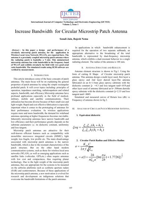
II. ANTENNA STRUCTURE AND RESULTS<br />
<strong>Antenna</strong> element structure is shown in Fig.1. Using the<br />
<strong>for</strong>m of cutting H Shape of <strong>Circular</strong> microstrip patch<br />
antenna. This antenna design a multi layer used, first layer a<br />
glass epoxy and 2nd layer duroid layer.The antenna<br />
fabricated on an h=1.5mm glass eproxy substrate with the<br />
dielectric constant ξr =4.3 and loss tangent tanδ=.019.and<br />
other layer used of antenna fabricated an h=.508mm duroide<br />
epoxy substrate with the dielectric constant ξr=2.33 and loss<br />
tangent tanδ=.0005.<br />
Simulated and measured curves of Return loss (db) vs<br />
Frequency of antenna shown in fig 2.<br />
III. ANALYSIS OF CIRCULAR PATCH MICROSTRIP ANTENNA.<br />
1. Equivalent dielectric<br />
<br />
r1 r2( h1 h2<br />
)<br />
eq<br />
<br />
h ( h h )<br />
r1 r2 1 1 2<br />
2. <strong>Circular</strong> <strong>Patch</strong> Radius and Effective Radius<br />
K<br />
a <br />
2<br />
f<br />
a<br />
e<br />
nm<br />
C<br />
<br />
eq<br />
2h<br />
a<br />
a{1 [ln( ) 1.7726]}<br />
a 2h<br />
eq<br />
1<br />
2<br />
169
ISSN 2249-6343<br />
International Journal of Computer Technology and Electronics Engineering (IJCTEE)<br />
Volume 2, Issue 1<br />
Fig1. Geometry of <strong>Circular</strong> <strong>Microstrip</strong> <strong>Patch</strong> <strong>Antenna</strong><br />
170
ISSN 2249-6343<br />
International Journal of Computer Technology and Electronics Engineering (IJCTEE)<br />
Volume 2, Issue 1<br />
Conductance<br />
The conductance due to the radiated power of the circular<br />
microstrip patch antenna can be computed based on the the<br />
radiated power expressed as;<br />
<br />
2 2 2<br />
V0 ( K0ae<br />
) 2 2 2<br />
Prad<br />
<br />
[ J '<br />
02<br />
cos J02]sind<br />
960<br />
<br />
0<br />
K 0 is the free space phase constant. The conductance across<br />
the gap between the patch and the ground plane at φ’=0o is<br />
given as<br />
2<br />
( Ka<br />
0 e) 3 2 2 1 4 4 7 6 6<br />
3 3 10<br />
Grad<br />
{[1 sin sin sin ]<br />
480 2 32 122<br />
3 2 2 1 4 4 7 6 6<br />
0.333[1 sin sin sin ]}<br />
3 3 10<br />
2 32 122<br />
Grad accounts <strong>for</strong> radiation and dielectric losses and are<br />
expressed as<br />
3 3<br />
2<br />
c<br />
m0 0 r 10 0 e<br />
2<br />
G ( ( f ) ) [( K a ) ]<br />
G<br />
d<br />
tan<br />
<br />
4 ( )<br />
m0<br />
2<br />
[( Kae) ]<br />
0h fr<br />
10<br />
as where G c is the conductance due to conduction losses, G d<br />
is the conductance due to dielectric losses and f r is the<br />
resonant frequency of the dominant mode. The total<br />
conductance can be expressed<br />
Gt Grad Gc Gd<br />
4.Directivity<br />
D<br />
0<br />
( Ka<br />
0 e)<br />
<br />
120G<br />
2<br />
rad<br />
This directivity is not strongly influenced by height of<br />
substrate as long as it is maintained electrically small. It is a<br />
function of patch radius.<br />
III.<br />
RESONANT INPUT IMPEDANCE<br />
The input impedance of a circular patch at resonance is real<br />
and the input power is independent of the feed point position<br />
on the circumference (Balanis, 1982). Taking the reference of<br />
the feed point at , the input resistance at any radial distance<br />
from the center of the patch can be written as (Balanis, 1982)<br />
J ( K<br />
)<br />
Rin <br />
G J Ka<br />
2<br />
1 [<br />
m 0<br />
2 ]<br />
t m( e)<br />
For the circular patch antenna, the resonant input resistance<br />
with an inset feed is<br />
2<br />
m<br />
in( ' 0) <br />
in( ' <br />
e)<br />
2<br />
Jm<br />
R R a<br />
J<br />
( K0)<br />
( Ka )<br />
PROGRAM DESIGN AND SIMULATION<br />
The program written in FORTRAN using WATFORT g77<br />
compiler was developed based on equations (17) to (35). The<br />
program was run on the DOS mode and results exported to<br />
Microsoft word.The main program reads in the microstrip<br />
parameters then determines the ideal radiation characteristics<br />
Input Parameters<br />
ξ eq = dielectric constant<br />
h= height of substrate<br />
C = Speed due to free space<br />
Output Parameters<br />
a = radius of patch<br />
a e = effective radius of patch<br />
G rad = Conductance between gap & ground<br />
G d = conductance due to dielectric<br />
G t = total conductance<br />
D 0 = directivity of slot<br />
R in = resonant of input resistance<br />
The calculate parameters <strong>for</strong> different antennas designed at<br />
various feeding point at a 5Ghz frequency are given in table:-<br />
<strong>Circular</strong> microstrip patch antenna results in table<br />
S.NO<br />
Co-Ordinates Result in dB <strong>Bandwidth</strong> Directivity<br />
1 -170,-292 -12db 7.6% 9.33db<br />
2 -122,-307 -18db 12% 6.88db<br />
3 -301,-149 -16db 12% 7.76db<br />
4 92,-2 -22db 28% 5.95db<br />
5 -140,-360 -14db 12% 9.57db<br />
6 -68,-323 -14db 22% 7.34db<br />
7 -81,-328 -14db 23% 6.71db<br />
8 95,0 -30db 34% 8.33db<br />
e<br />
171
ISSN 2249-6343<br />
International Journal of Computer Technology and Electronics Engineering (IJCTEE)<br />
Volume 2, Issue 1<br />
IV. RESULTS<br />
The simulated results of the antenna comprise of return loss(db).Fabricated antenna at frequency 5GHz.<br />
simulated<br />
Frequency GHz<br />
Fig2.-GHz <strong>Antenna</strong> Results<br />
Fig3.-Simulated VSWR vs.Frequency of antenna<br />
172
ISSN 2249-6343<br />
International Journal of Computer Technology and Electronics Engineering (IJCTEE)<br />
Volume 2, Issue 1<br />
V. CONCLUSION<br />
This study provided an insight in determining the<br />
per<strong>for</strong>mance of microstrip patch antenna. From the results<br />
presented it is observed that glass epoxy and duroid epoxy<br />
<strong>for</strong> X-band antenna designs . However,first theoretically<br />
calculated parametric dimensions and simulated results<br />
should be properly analyzed. Then based on the<br />
analysis,predesign calibrating corrections may be<br />
incorporated in the bandwidth development<br />
process.predesign bandwidth are maximum 15% and this<br />
paper of bandwidth 34% .It means 19%bandwidth<br />
improvement this paper.<br />
ACKNOWLEDGEMENTS<br />
The authors, <strong>for</strong> this work, deeply acknowledge the<br />
professional guidance provided by Mr. Rajesh Nema , and<br />
financial support by NIIST. The authors also sincerely<br />
recognize technical help and day to day supported.<br />
REFERENCES<br />
[1]. Al-Zoubi, F. Yang, and A. Kishk, “A broadband center-fed<br />
circular patch-ring antenna with a monopole like radiation<br />
pattern,” IEEE Trans. <strong>Antenna</strong>s Propag., vol. 57, pp.<br />
789–792, 2009.<br />
[2]. M. John and M. J. Ammann, “Wideband printed monopole<br />
design using a genetic algorithm,” IEEE <strong>Antenna</strong>s Wireless<br />
Propag. Lett. vol.6, pp. 447–449, 2007.<br />
[3]. S. K. Oh, H. S. Yoon, and S. O. Park, “A PIFA-type<br />
varactor-tunable slim antenna with a PIL patch feed <strong>for</strong><br />
multiband applications,” IEEE <strong>Antenna</strong>s Wireless Propag.<br />
Lett., vol. 6, pp. 103–105, 2007.<br />
[4]. C. H. Chang and K. L. Wong, “Printed -PIFA <strong>for</strong> penta-band<br />
WWAN operation in the mobile phone,” IEEE Trans.<br />
<strong>Antenna</strong>s Propag., vol. 57, pp. 1373–1381, 2009.<br />
[5]. Nasimuddin and Z. N. Chen, “Wideband multilayered<br />
microstrip antennas fed by coplanar waveguide-loop with<br />
and without via combinations,” IET Microw. <strong>Antenna</strong>s<br />
Propag., vol. 3, pp. 85–91, 2009.<br />
[6]. W. C. Liu, “Design of a multiband CPW-fed monopole<br />
antenna using a particle swarm optimization approach,”<br />
IEEE Trans. <strong>Antenna</strong>s Propag., vol. 53, pp. 3273–3279,<br />
2005.<br />
173