SJ300 & L300P Series Inverters Service Manual : Hitachi America, Ltd.
SJ300 & L300P Series Inverters Service Manual : Hitachi America, Ltd.
SJ300 & L300P Series Inverters Service Manual : Hitachi America, Ltd.

Create successful ePaper yourself
Turn your PDF publications into a flip-book with our unique Google optimized e-Paper software.
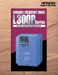
HITACHI INVERTER<br />
<strong>SJ300</strong> / <strong>L300P</strong> SERIES<br />
SERVICE MANUAL<br />
After reading this manual , keep it hand for future reference.<br />
H I T A C H I<br />
NBS611CX
Revision History Table<br />
No.<br />
Revision Contents<br />
The Date<br />
of Issue<br />
Operation<br />
<strong>Manual</strong> No.<br />
1 Japanese font was removed. Nov. 2000 NBS611BX<br />
2 The specification of the capacity 75-132kW and more was added. Mar. 2001 NBS611CX
Table of contents<br />
1. Investigation of the inverter<br />
1.1 Specification label(Model name , Manufacturing number ; MFG)<br />
1.1.1 Model name <br />
1-1<br />
1.1.2 MFG number <br />
1-1<br />
1.2 Inverter specification<br />
1.2.1 <strong>SJ300</strong> <br />
1-2<br />
1.2.2 <strong>L300P</strong> <br />
1-10<br />
2. Trouble shooting<br />
2.1 INV trip contents , remedy , advice <br />
2-1<br />
2.2 Option error<br />
2.2.1 Feed-back board (SJ-FB) <br />
2-3<br />
2.2.2 Digital-input option board (SJ-DG)<br />
2-3<br />
2.2.3 Device-Net option board (SJ-DN)<br />
2-3<br />
2.3 Check of the trip monitor contents <br />
2-4<br />
2.4 Confirmation of the warning monitor contents <br />
2-5<br />
2.5 Return to an initialization setup (Factory-shipment state) <br />
2-6<br />
3. Debug mode<br />
3.1 Monitor mode <br />
3-1<br />
3.2 Function mode<br />
3-2<br />
3.3 Parameter settings for inverter <br />
3-3<br />
4. The check of control power supply voltage and a control signal<br />
4.1 Control power supply voltage <br />
4-1<br />
4.2 Control signal <br />
4-1<br />
5. Maintenance and Inspection<br />
5.1 Maintenance and Inspection<br />
5.1.1 Daily inspection <br />
5-1<br />
5.1.2 Cleaning <br />
5-1<br />
5.1.3 Periodical inspection <br />
5-1<br />
5.2 Daily and annual maintenance <br />
5-2<br />
5.3 Megger test <br />
5-3<br />
5.4 Withstand voltage test <br />
5-3<br />
5.5 How to check inverter , converter , BR and Thyristor portion <br />
5-4<br />
5.6 Parts replacement <br />
5-5<br />
5.7Unit replacement <br />
5-8<br />
Appendix<br />
Circuit Diagram<br />
Internal block diagram<br />
Structure figure
1. Investigation of the inverter<br />
1.1 Specification label (Model name, Manufacturing number ; MFG)<br />
• There are 2 specification label attached to the inverter as shown in Fig 1-1.<br />
Specification label<br />
Fig 1-1 Specification label location<br />
• Please confirm the model name and MFG number from the specification label as follows.<br />
Model name<br />
Applicable motor<br />
Input ratings<br />
Output ratings<br />
MFG number<br />
1.1.1 Model name<br />
<strong>SJ300</strong>-055 H F (R)<br />
Fig 1-2 contents of specification label<br />
R : with POT meter<br />
F : with digital operator<br />
Model name<br />
L : 3 φ 200V class<br />
H : 3 φ 400V class<br />
Applicable motor (055 : 5.5kW)<br />
1.1.2 MFG number<br />
94 A T12345 9 0001<br />
Serial No. (0001 ~ 9999)<br />
Year of production (9 : 1999)<br />
Production No.<br />
REV. No.(1 character or 2 characters)<br />
Production year & month (94 : 1999 / April)<br />
1-1
1.2 Inverter specification<br />
1.2.1 <strong>SJ300</strong><br />
Monitor Mode<br />
Display<br />
code<br />
d001<br />
d002<br />
d003<br />
d004<br />
d005<br />
d006<br />
Function name<br />
Output frequency<br />
monitor<br />
Output current<br />
monitor<br />
Operation direction<br />
monitor<br />
PID feedback<br />
monitor<br />
Intelligent input<br />
terminal monitor<br />
Intelligent output<br />
terminal monitor<br />
<strong>SJ300</strong> monitor or data range<br />
(digital operator)<br />
Initial<br />
data<br />
0.00-99.99/100.0-400.0(Hz) -<br />
0.0-999.9(A) -<br />
F(forward)/o(stop)/r(reverse) -<br />
0.00-99.99/100.0-999.9/1000. – 9999. /<br />
1000-9999/ 100- 999 (10000-99900)<br />
8<br />
FW<br />
7 6<br />
(Example) FW, terminal 7,2, 1: ON<br />
Terminal 8,6,5,4,3:OFF<br />
ON<br />
OFF<br />
5 4 3 2 1<br />
AL 15 14 13 12<br />
(Example) Terminal 12,11:ON<br />
AL, 15,14,13:OFF<br />
ON<br />
d007<br />
Frequency<br />
0.00-99.99/100.0-999.9/1000. – 9999. /<br />
conversion monitor 1000-3996<br />
-<br />
d012 torque monitor -300.-+300.% -<br />
d013<br />
Output voltage<br />
monitor<br />
0.0-600.0 V -<br />
d014<br />
Input electric power<br />
monitor<br />
0.0-999.9 kW -<br />
Accumulated time<br />
d016 monitor during 0.-9999./1000-9999/ 100- 999 h -<br />
RUN<br />
d017<br />
Power ON time<br />
monitor<br />
0.-9999./1000-9999/ 100- 999 h -<br />
d080<br />
Number of trip time<br />
monitor<br />
0.-9999./1000-6553(10000-65530) (time) -<br />
d081 Trip monitor 1 -<br />
d082 Trip monitor 2 -<br />
d083 Trip monitor 3 Trip Code, frequency(Hz), current(A), -<br />
d084 Trip monitor 4 voltage(V),RUN time(h) power ON time(h) -<br />
d085 Trip monitor 5 -<br />
d086 Trip monitor 6<br />
-<br />
d090 Warning monitor Warning code -<br />
F001<br />
Output frequency 0.0, starting frequency-Max. frequency<br />
setting<br />
(2 nd max. 3 rd max. frequency)(Hz)<br />
0.00<br />
F002 1 st acceleration time 0.01-99.99/100.0-999.9/1000. -3600.(s) 30.00<br />
F202 2 nd acceleration time 0.01-99.99/100.0-999.9/1000. -3600.(s) 30.00<br />
F302 3 rd acceleration time 0.01-99.99/100.0-999.9/1000. -3600.(s) 30.00<br />
F003 1 st deceleration time 0.01-99.99/100.0-999.9/1000. -3600.(s) 30.00<br />
F203 2 nd deceleration time 0.01-99.99/100.0-999.9/1000. -3600.(s) 30.00<br />
F303 3 rd deceleration time 0.01-99.99/100.0-999.9/1000. -3600.(s) 30.00<br />
F004<br />
Operation direction<br />
selection<br />
00(forward)/01(reverse) 00<br />
(Note1) Change mode during run by selection of b031 (software lock selection).<br />
(Note2) Do not forget to press “STR” key when you change the display.<br />
OFF<br />
-<br />
-<br />
-<br />
(Note1)<br />
Note<br />
1–2
Function Mode<br />
Base setting<br />
Analog input setting<br />
Multistage speed,jogging frequency setting<br />
Direct current braking<br />
V/f characteristic<br />
Code Function name <strong>SJ300</strong> Setting range<br />
Initial data<br />
-FE/-FU/-F<br />
A001 Frequency setting selection 01(terminal)/02(operator)/03(RS485)/04(option1)/05(option2) 01/01/02<br />
A002 Operation setting selection 01(terminal)/02(operator)/03(RS485)/04(option1)/05(option2) 01/01/02<br />
A003 Base frequency 30. - Maximum. frequency(Hz) 50./60./60.<br />
A203 Base frequency, 2nd motor 30. – 2nd Maximum. frequency (Hz) 50./60./60.<br />
A303 Base frequency, 3rd motor 30. - 3rd Maximum. frequency (Hz) 50./60./60.<br />
A004 Maximum frequency 30. – 400. (Hz) 50./60./60.<br />
A204 Maximum frequency, 2nd motor 30. – 400. (Hz) 50./60./60.<br />
A304 Maximum frequency, 3rd motor 30. – 400. (Hz) 50./60./60.<br />
A005 AT terminal selection<br />
00( Changing of O and OI with AT terminal)/<br />
01(Changing of O and O2 with AT terminal)<br />
00<br />
A006 02 selection<br />
00(single)/01(auxiliary speed of O, OI) [no reversible] /<br />
02(auxiliary speed of O, OI [reversible]<br />
00<br />
A011 0 start 0.00-99.99/100.0-400.0 (Hz) 0.00<br />
A012 0 end 0.00-99.99/100.0-400.0 (Hz) 0.00<br />
A013 0 start rate 0.-100.0 (%) 0.<br />
A014 0 end rate 0.-100.0(%) 100.<br />
A015 0 start selection 00 (external starting frequency)/01(0Hz) 01<br />
A016 O, OI, O2 sampling 1.-30.(times) 8.<br />
A019 Multi-speed selection<br />
00(binary : range is to 16 stage speed with 4 terminals)/<br />
01(bit : range is to 8 stage speed with 7 terminals)<br />
00<br />
A020 Multi-speed 0 0.00, starting frequency-maximum. frequency(Hz) 0.00<br />
A220 Multi-speed 0, 2 nd motor 0.00, starting frequency-2 nd maximum frequency(Hz) 0.00<br />
A320 Multi-speed 0, 3 rd motor 0.00, starting frequency-3 rd maximum frequency(Hz) 0.00<br />
A021 Multi-speed1 0.00, starting frequency-maximum frequency(Hz) 0.00<br />
A022 Multi-speed2 0.00, starting frequency-maximum frequency(Hz) 0.00<br />
A023 Multi-speed3 0.00, starting frequency-maximum frequency(Hz) 0.00<br />
A024 Multi-speed4 0.00, starting frequency-maximum frequency(Hz) 0.00<br />
A025 Multi-speed5 0.00, starting frequency-maximum frequency(Hz) 0.00<br />
A026 Multi-speed6 0.00, starting frequency-maximum frequency(Hz) 0.00<br />
A027 Multi-speed7 0.00, starting frequency-maximum frequency(Hz) 0.00<br />
A028 Multi-speed8 0.00, starting frequency-maximum frequency(Hz) 0.00<br />
A029 Multi-speed9 0.00, starting frequency-maximum frequency(Hz) 0.00<br />
A030 Multi-speed10 0.00, starting frequency-maximum frequency(Hz) 0.00<br />
A031 Multi-speed11 0.00, starting frequency-maximum frequency(Hz) 0.00<br />
A032 Multi-speed12 0.00, starting frequency-maximum frequency(Hz) 0.00<br />
A033 Multi-speed13 0.00, starting frequency-maximum frequency(Hz) 0.00<br />
A034 Multi-speed14 0.00, starting frequency-maximum frequency(Hz) 0.00<br />
A035 Multi-speed15 0.00, starting frequency-maximum frequency(Hz) 0.00<br />
A038 Jogging frequency 0.00, starting frequency-9.99(Hz) 1.00<br />
A039 Jogging selection<br />
00(free-run on JG stop / invalid on running) / 01(stop decelerating on<br />
JG stop / invalid on running) / 02(DC braking on JG stop/invalid on<br />
running) / 03(free-run on JG stop/valid on running[JG after stop 00<br />
decelerating]) / 04 (stop decelerating on JG stop/valid on running) / 05<br />
(DC braking on JG stop/valid on operating)<br />
A041 Torque boost selection 00 (manual torque boost) / 01 (automatic torque boost) 00<br />
A241<br />
Torque boost selection, 2 nd<br />
motor<br />
00 (manual torque boost) / 01 (automatic torque boost) 00<br />
A042 <strong>Manual</strong> torque boost 0.0-20.0(%) 1.0<br />
A242 <strong>Manual</strong> torque boost, 2 nd motor 0.0-20.0(%) 1.0<br />
A342 <strong>Manual</strong> torque boost, 3 rd motor 0.0-20.0(%) 1.0<br />
A043 <strong>Manual</strong> torque boost point 0.0-50.0(%) 5.0<br />
A243<br />
<strong>Manual</strong> torque boost point, 2 nd<br />
motor<br />
0.0-50.0(%) 5.0<br />
A343<br />
<strong>Manual</strong> torque boost point, 3 rd<br />
motor<br />
0.0-50.0(%) 5.0<br />
A044 1 st control<br />
00/(VC)/01(VP1.7power)/02(free V/f setting)/03(SLV)/<br />
04(0Hz-SLV)/05(V2)<br />
00<br />
A244 2 nd control 00/(VC)/01(VP1.7power)/02(free V/f setting) /03(SLV)/04(0Hz-SLV) 00<br />
A344 3 rd control 00/(VC)/01(VP1.7power) 00<br />
A045 Output voltage gain 20. - 100. 100.<br />
A051 DC braking selection 00(invalid)/01(valid) 00<br />
A052 DC braking frequency 0.00-60.00(Hz) 0.50<br />
A053 DC braking wait time 0.0 - 5.0(s) 0.0<br />
A054 DC braking power 0. - 100. (%) 0.<br />
A055 DC braking time 0.0 - 60.0(s) 0.0<br />
A056 DC braking edge/level selection 00(edge action)/01(level action) 01<br />
A057 DC braking power (starting time) 0. - 100. (%) 0.<br />
A058 DC braking time(starting time) 0.00-60.0(s) 0.0<br />
A059 DC carrier frequency 0.5-15(kHz) Derating 5.0<br />
(Note) < > indicate the setting range of 75 to 150kW<br />
Note<br />
1- 3
Upper and lower limiter,jump<br />
frequency<br />
PID control<br />
AVR<br />
Operation mode/ adjustable function<br />
External frequency<br />
adjustment<br />
Accel,<br />
Decel<br />
Instantaneous power failure<br />
restart<br />
Function Mode<br />
Initial data<br />
Code Function name <strong>SJ300</strong> Setting range<br />
-FE/-FU/-F<br />
A061 1 st frequency maximum limiter 0.00, 1 st frequency lower limitter - maximum frequency(Hz) 0.00<br />
A261 2 nd frequency maximum limiter 0.00, 2 nd frequency lower limiter-2 nd setting maximum frequency(Hz) 0.00<br />
A062 1 st frequency minimum limiter 0.00, start frequency-maximum frequency(Hz) 0.00<br />
A262 2 nd frequency minimum limiter 0.00, start frequency-2 nd setting maximum frequency(Hz) 0.00<br />
A063 Jump frequency1 0.00-99.99/100.0-400.0(Hz) 0.00<br />
A064 Jump frequency Width 1 0.00-10.00(Hz) 0.50<br />
A065 Jump frequency2 0.00-99.99/100.0-400.0(Hz) 0.00<br />
A066 Jump frequency Width 2 0.00-10.00(Hz) 0.50<br />
A067 Jump frequency3 0.00-99.99/100.0-400.0(Hz) 0.00<br />
A068 Jump frequency Width 3 0.00-10.00(Hz) 0.50<br />
A069 Acceleration stop frequency 0.00-99.99/100.0-400.0(Hz) 0.00<br />
A070 Acceleration stop time 0.00-60.0(s) 0.0<br />
A071 PID selection 00(invalid)/01(valid) 00<br />
A072 PID-P gain 0.2-5.0 1.0<br />
A073 PID-I gain 0.0-3600.(s) 1.0<br />
A074 PID-D gain 0.00-100.0(s) 0.00<br />
A075 PID scale 0.01-99.99(%) 1.00<br />
A076 PID feedback selection 00(feedback : OI)/01(feedback : O) 00<br />
A081 AVR selection 00(ON always)/01(OFF always)/02(OFF on decelerating) 00/00/02<br />
(230/400)/<br />
A082 Motor voltage selection 200/215/220/230/240, 380/400/415/440/460/480<br />
(230/460)/<br />
(200/400)<br />
A085 Operation mode selection 00(normal operation)/01(energy-saving operation)/02(Fuzzy) 00<br />
A086<br />
Energy-saving responseaccuracy<br />
adjustment<br />
0.0-100.0 50.0<br />
A092 Acceleration time2 0.01-99.99/100.0-999.9/1000.-3600.(s) 15.00<br />
A292 Acceleration time2(2 nd motor) 0.01-99.99/100.0-999.9/1000.-3600.(s) 15.00<br />
A392 Acceleration time2(3 rd motor) 0.01-99.99/100.0-999.9/1000.-3600.(s) 15.00<br />
A093 Deceleration time2 0.01-99.99/100.0-999.9/1000.-3600.(s) 15.00<br />
A293 Deceleration time2(2 nd motor) 0.01-99.99/100.0-999.9/1000.-3600.(s) 15.00<br />
A393 Deceleration time2(3 rd motor) 0.01-99.99/100.0-999.9/1000.-3600.(s) 15.00<br />
A094 2 nd stage adjustable selection 00(change with 2CH terminal)/01(change with setting) 00<br />
A294<br />
2 nd stage adjustable<br />
selection(2 nd motor)<br />
00(change with 2CH terminal)/01(change with setting) 00<br />
A095 2 nd acceleration frequency 0.00-99.99/100.0-400.0(Hz) 0.00<br />
A295<br />
2 nd acceleration<br />
frequency(2 nd motor)<br />
0.00-99.99/100.0-400.0(Hz) 0.00<br />
A096 2 nd deceleration frequency 0.00-99.99/100.0-400.0(Hz) 0.00<br />
A296<br />
2 nd deceleration frequency<br />
(2 nd motor)<br />
0.00-99.99/100.0-400.0(Hz) 0.00<br />
A097 Acceleration pattern selection 00(straight line)/01(S-curve)/02(U-curve)/03(reverse U-curve) 00<br />
A098 Deceleration pattern selection 00(straight line)/01(S-curve)/02(U-curve)/03(reverse U-curve) 00<br />
A101 OI start 0.00-99.99/100.0-400.0(Hz) 0.00<br />
A102 OI end 0.00-99.99/100.0-400.0(Hz) 0.00<br />
A103 OI start rate 0.-100. (%) 20.<br />
A104 OI end rate 0.-100. (%) 100.<br />
A105 OI start selection 00(external start frequency)/01(0Hz) 01<br />
A111 O2 start -400.--100./-99.9-0.00-99.9/100.-400.(Hz) 0.00<br />
A112 O2 end -400.--100./-99.9-0.00-99.9/100.-400.(Hz) 0.00<br />
A113 O2 start rate -100. - 100. (%) -100.<br />
A114 O2 end rate -100. - 100. (%) 100.<br />
A131 Acceleration curve constant 01(small swelling)-10(large swelling) 02<br />
A132 Deceleration curve constant 01(small swelling-10(large swelling) 02<br />
b001 Retry selection<br />
00(trip)/01(0Hz start)/02(start after equal frequency)/<br />
03(trip after equaling frequency and deceleration stop)<br />
00<br />
b002<br />
Allowable under-voltage power<br />
failure time<br />
0.3-1.0(s) 1.0<br />
b003 Retry wait time 0.3-100.(s) 1.0<br />
b004<br />
Instantaneous power failure/ 00(invalid/01(valid)/02(invalid during stop and deceleration by stop<br />
under-voltage trip during stop<br />
command)<br />
00<br />
b005<br />
Instantaneous power failure/<br />
under-voltage retry time<br />
00(16 times)/01(free) 00<br />
selection<br />
b006 Open-phase selection 00(invalid)/01(valid) 00<br />
b007 Frequency setting to match 0.00-99.99/100.0-400.0(Hz) 0.00<br />
Note<br />
1- 4
Electronic thermal<br />
Intelligent input terminal setting Free V/f setting<br />
Overload limit<br />
Function mode<br />
Code Function name <strong>SJ300</strong> Setting range<br />
b012 Electronic thermal level 0.2*constant current-1.20*constant current(A)<br />
b212<br />
b312<br />
b013<br />
b213<br />
b313<br />
b015<br />
b016<br />
b017<br />
b018<br />
b019<br />
b020<br />
b021<br />
Electronic thermal level<br />
(2 nd motor)<br />
Electronic thermal level<br />
(3 rd motor)<br />
1 st electronic thermal<br />
characteristic selection<br />
2 nd electronic thermal<br />
characteristic selection<br />
3 rd electronic thermal<br />
characteristic selection<br />
Free electronic thermal<br />
frequency 1<br />
Free electronic thermal<br />
current 1<br />
Free electronic thermal<br />
frequency 2<br />
Free electronic thermal<br />
current 2<br />
Free electronic thermal<br />
frequency 3<br />
Free electronic thermal<br />
current 3<br />
Overload restriction selection<br />
0.2*constant current-1.20*constant current(A)<br />
0.2*constant current-1.20*constant current(A)<br />
00(reduced characteristic)/ 01(constant torque characteristic)/<br />
02(free setting)<br />
00(reduced characteristic)/ 01(constant torque characteristic)/<br />
02(free setting)<br />
00/(reduced characteristic)01(constant torque characteristic)/<br />
02(free setting)<br />
Initial data<br />
-FE/-FU/-F<br />
Rated<br />
Current of<br />
inverter<br />
Rated<br />
Current of<br />
Inverter<br />
Rated<br />
current of<br />
inverter<br />
01/01/00<br />
01/01/00<br />
01/01/00<br />
0.-400.(Hz) 0.<br />
0.0-1000.(A) 0.0<br />
0.-400.(Hz) 0.<br />
0.0-1000. (A) 0.0<br />
0.-400.(Hz) 0.<br />
0.0-1000.(A) 0.0<br />
00(invalid)/01(enabled on acceleration / constant speed)/<br />
02(enabled on constant speed)/03(enabled on acceleration / constant<br />
speed (speed increasing at regenerating mode))<br />
b022 Overload restriction level 0.50* rated current-2.00* rated current(A) <br />
b023<br />
b024<br />
Overload restriction limit<br />
constant<br />
Overload restriction 2<br />
selection<br />
01<br />
Rated current<br />
of Inverter<br />
x 1.50<br />
0.10-30.00(s) 1.00<br />
00(invalid)/01(enabled on acceleration / constant speed)/<br />
02(enabled on constant speed)/03(enabled on acceleration / constant<br />
speed (speed increasing at regenerating mode))<br />
b025 Overload restriction level 2 0.50*rated current-2.00*rated current(A) <br />
b026<br />
b031<br />
Overload restriction constant<br />
2<br />
Software lock mode selection<br />
01<br />
Rated current<br />
of inverter<br />
x1.50<br />
0.10-30.00(s) 1.00<br />
00(impossible to change the data except this item when SFT terminal is<br />
ON)/01(impossible to change the data except setting frequency item<br />
when SFT terminal is ON)/02(impossible to change the data except this<br />
item)/<br />
03(impossible to change the data except setting frequency item)/<br />
10(possible to change data on operating)<br />
b100 Free V/f frequency 1 0.- Free V/f frequency2(Hz) 0.<br />
b101 Free V/f voltage 1 0.-800.0(V) 0.0<br />
b102 Free V/f frequency 2 0.- Free V/f frequency3(Hz) 0.<br />
b103 Free V/f voltage 2 0.-800.0(V) 0.0<br />
b104 Free V/f frequency 3 0.- Free V/f frequency4(Hz) 0.<br />
b105 Free V/f voltage 3 0.-800.0(V) 0.0<br />
b106 Free V/f frequency 4 0.- Free V/f frequency5(Hz) 0.<br />
b107 Free V/f voltage 4 0.-800.0(V) 0.0<br />
b108 Free V/f frequency 5 0.- Free V/f frequency6(Hz) 0.<br />
b109 Free V/f voltage 5 0.-800.0(V) 0.0<br />
b110 Free V/f frequency 6 0.- Free V/f frequency7(Hz) 0.<br />
b111 Free V/f voltage 6 0.-800.0(V) 0.0<br />
b112 Free V/f frequency 7 0.-400.(Hz) 0.<br />
b113 Free V/f voltage 7 0.-800.0(V) 0.0<br />
01/(RV:Reverse is valid)/02(CF1:Multi-speed1)/ 03(CF2:Multi-speed2)/<br />
C001 Intelligent input 1 setting<br />
04(CF3:Multi-speed3)/ 05(CF4:Multi-speed4)/ 06(JG:Jogging)/<br />
18<br />
07( DB:External DC braking)/ 08(SET:2 nd control)/<br />
C002 Intelligent input 2 setting<br />
09(2CH:two-stage adjustable speed)/ 11( FRS:Free-run)/ 12( EXT:External trip)/<br />
16<br />
13( USP:Unattended start protection)/ 14(CS:commercial change)/<br />
15(SFT:software lock)/ 16(AT:Analog input voltage/current select)/<br />
C003 Intelligent input 3 setting 17(SET3:3 rd control)/ 18(RS:Reset inverter)/ 20(STA:3wire run)/<br />
06<br />
21(STP:3wire keep)/ 22(F/R:3wire forward/reverse)/<br />
23(PID:PID selection valid/invalid)/ 24(PIDC:PID integrating reset)/<br />
C004 Intelligent input 4 setting 26( CAS:Control gain switch function)/ 27( UP:Remote control UP function)/ 11<br />
28( DWN:Remote control DOWN function)/29( UDC:Remote control data clear)/<br />
31( OPE:Operating by operator select)/ 32(SF1:Multi-speed bit1)/<br />
C005 Intelligent input 5 setting 33(SF2:Multi-speed bit2)/ 34(SF3:Multi-speed bit3)/ 35(SF4:Multi-speed bit4)/ 09<br />
36(SF5:Multi speed bit5)/ 37(SF6:Multi-speed bit6)/ 38(SF7:Multi-speed bit7)/<br />
C006 Intelligent input 6 setting 39( OLR:Overload restriction change) / 40(TL:Torque limit select)/<br />
03/13/03<br />
41(TRQ1:Torque limit switch 1)/ 42(TRQ2:Torque limit switch 2)/<br />
C007 Intelligent input 7 setting 43((PPI:P/PI switch)/ 44(BOK:Braking comformation)/ 45( ORT:Orientation)/ 02<br />
C008 Intelligent input 8 setting<br />
46(LAC:LAD cancel)/ 47(PCLR:Position error clear)/<br />
48(STAT:Permission of pulse train)/ no(NO:No assign)<br />
01<br />
(Note) < > indicate the setting range of 75 to 150kW<br />
01<br />
Note<br />
1- 5
Input terminal setting<br />
intelligent<br />
Communication<br />
Output terminal state<br />
Analog meter setting function adjustment<br />
setting,Output level setting<br />
Intelligent output terminal setting<br />
Function mode<br />
Code Function name <strong>SJ300</strong> Setting range<br />
Initial data<br />
-FE/-FU/-F<br />
C011<br />
Intelligent input 1 a/b<br />
(NO/NC) selection<br />
00(NO)/01(NC) 00<br />
C012<br />
Intelligent input 2 a/b<br />
(NO/NC) selection<br />
00(NO)/01(NC) 00<br />
C013<br />
Intelligent input 3 a/b<br />
(NO/NC) selection<br />
00(NO)/01(NC) 00<br />
C014<br />
Intelligent input 4 a/b<br />
(NO/NC) selection<br />
00(NO)/01(NC) 00<br />
C015<br />
Intelligent input 5 a/b<br />
(NO/NC) selection<br />
00(NO)/01(NC) 00<br />
C016<br />
Intelligent input 6 a/b<br />
(NO/NC) selection<br />
00(NO)/01(NC) 00/01/00<br />
C017<br />
Intelligent input 7a/b<br />
(NO/NC) selection<br />
00(NO)/01(NC) 00<br />
C018<br />
Intelligent input 8 a/b<br />
(NO/NC) selection<br />
00(NO)/01(NC) 00<br />
C019<br />
Input FW a/b (NO/NC)<br />
Selection<br />
00(NO)/01(NC) 00<br />
00(RUN:running)/01(FA1:Frequency arrival type1 signal)/<br />
C021 Intelligent output 11 setting 02(FA2:over setting frequency)/03( OL:Overload advance notice signal)/ 01<br />
C022 Intelligent output 12 setting<br />
04( OD:Output deviation for PID control)/05( AL:Alarm signal)/<br />
06(FA3:Only setting frequency)/07( OTQ:Over-torque signal)/<br />
08( IP:On instantaneous stop)/09(UV:Under voltage)/<br />
00<br />
C023 Intelligent output 13 setting<br />
10(TRQ:Torque limit)/11(RNT:RUN time over/12(ONT:ON time over)/<br />
13(THM:thermal caution)/19(BRK:Brake release signal)/<br />
03<br />
C024 Intelligent output 14 setting<br />
20( BER:Brake error signal)/21(ZS:Zero speed detect signal)/<br />
22(DSE:Speed error over signal)/23(POK:Positioning completion signal)<br />
07<br />
C025 Intelligent output 15 setting<br />
24(FA4:Over frequency 2 signal)/25(FA5:Only setting frequency)/<br />
26(OL2: Overload advance notice signal 2)<br />
08<br />
C026 Alarm relay output<br />
(Intelligent output terminal 11-13 or 11-14 becomes AC0-AC2 or AC0-AC3<br />
(Can:Alarm cord output) forcibly when alarm cord output is selected in 05<br />
C062)<br />
C027 FM selection<br />
00(Output frequency)/01(Output current) /02(Output torque)/<br />
03(Digital output frequency)/04(Output voltage)/<br />
00<br />
05(Input electric power)/06(thermal load rate)/07(LAD frequency)<br />
C028 AM selection<br />
00(Output frequency)/01(Output current)/02(Output torque)/<br />
04(Output voltage)/05(Input electric power)/06(thermal load rate)/<br />
00<br />
07(LAD frequency)<br />
C029 AMI selection<br />
00(Output frequency)/01(Output current)/02(Output torque)/<br />
04(Output voltage)/05(Input electric power)/<br />
00<br />
06(Thermal load rate)/07(LAD frequency)<br />
C031 Intelligent output 11 a/b 00(NO)/01(NC) 00<br />
C032 Intelligent output 12 a/b 00(NO)/01(NC) 00<br />
C033 Intelligent output 13 a/b 00(NO)/01(NC) 00<br />
C034 Intelligent output 14 a/b 00(NO)/01(NC) 00<br />
C035 Intelligent output 15 a/b 00(NO)/01(NC) 00<br />
C036 Alarm relay output a/b 00(NO)/01(NC) 01<br />
C040<br />
Overload advance notice<br />
signal output mode<br />
00(On accel. And decel, constant speed)/01(Only constant speed) 01<br />
C041<br />
Overload advance notice<br />
Inverter<br />
0.0-2.0*rated current(A)<br />
level<br />
rated current<br />
C042<br />
Frequency arrival setting for<br />
acceleration.<br />
0.00-99.99/100.0-400.0(Hz) 0.00<br />
C043<br />
Arrival frequency setting for<br />
deceleration.<br />
0.00-99.99/100.0-400.0(Hz) 0.00<br />
C044 PID deviation setting level 0.0-100.0(%) 3.0<br />
C045<br />
Frequency arrival setting for<br />
acceleration 2.<br />
0.00-99.99/100.0-400.0(Hz) 0.00<br />
C046<br />
Arrival frequency setting for<br />
deceleration 2.<br />
0.00-99.99/100.0-400.0(Hz) 0.00<br />
C055<br />
Over torque level setting<br />
(Forward-driving)<br />
0.-200.(%) 100.<br />
C056<br />
Over torque level setting<br />
(Reverse-regenerating)<br />
0.-200.(%) 100.<br />
C057<br />
Over torque level setting<br />
(Reverse-driving)<br />
0.-200.(%) 100.<br />
C058<br />
Over torque level setting<br />
(Forward-regenerating)<br />
0.-200.(%) 100.<br />
C061<br />
Thermal warning level<br />
setting<br />
0.-100.(%) 80.<br />
C062 Alarm code selection 00(Invalid)/01(3bit)/02(4bit) 00<br />
C063<br />
Zero speed detection level<br />
setting<br />
0.00-99.99/100.(Hz) 0.00<br />
C070 Data command 02(operator)/03(RS485)/04(option1)/05(option2) 02<br />
C071<br />
Communicating transmission<br />
02(loop-back test)<br />
speed<br />
03(2400bps)/04(4800bps)/05(9600bps)/06(19200bps)<br />
04<br />
C072 Communication code 1. -32. 1.<br />
C073 Communication bit 7(7bit)/8(8bit) 7<br />
C074 Communication parity 00(no parity name)/01(even parity)/02(odd parity) 00<br />
C075 Communication stop bit 1(bit)/2(bit) 1<br />
C078 Communication waiting time 0.-1000.(ms) 0.<br />
C081 O adjustment 0.-9999./1000-6553(10000-65530)<br />
Setting on<br />
forwarding<br />
C082 OI adjustment 0.-9999./1000-6553(10000-65530)<br />
Setting on<br />
forwarding<br />
C083 O2 adjustment 0.-9999./1000-6553(10000-65530)<br />
Setting on<br />
forwarding<br />
C085 Thermistor adjustment 0.0 - 1000. 105.0<br />
C086 AM offset adjustment 0.0 - 10.0(V) 0.0<br />
C087 AMI adjustment 0. - 255. 80<br />
C088 AMI offset adjustment 0. - 20.0( mA) 4.0<br />
(Note) < > indicate the setting range of 75 to 150kW<br />
Note<br />
1- 6
The others<br />
Function mode<br />
Code Function name <strong>SJ300</strong> Setting range<br />
Initial data<br />
-FE/-FU/-F<br />
b034 RUN time/Power ON time level 0.-9999./1000-6553(10000-65530)hr 0.<br />
b035 Operation direction restrict 00(Reverse is valid)/01(Only forward)/02(Only reverse) 00<br />
b036 Start reduced voltage 00(Start reduced voltage time small)-06(Start reduced voltage time large) 06<br />
b037 Display selection 00(all display)/01(each function display)/02(User setting / main setting) 00<br />
b040 Torque limit mode selection<br />
00(4 quadrant mode)/01(Terminal operation)/<br />
02(Analog input)/03(Option1)/04(Option2)<br />
00<br />
b041<br />
Torque limit level 1 setting<br />
(Forward-driving at<br />
0.-200.(%)/no(Invalid) 150.<br />
4 quadrant mode)<br />
b042<br />
Torque limit level 2 setting<br />
(Reverse-regenerating at<br />
0.-200.(%)/no(Invalid) 150.<br />
4 quadrant mode)<br />
b043<br />
Torque limit level 3 setting<br />
(Reverse-driving at<br />
0.-200.(%)/no(Invalid) 150.<br />
4 quadrant mode)<br />
b044<br />
Torque limit level 4 setting<br />
(Forward-regenerating at<br />
0.-200.(%)/no(Invalid) 150.<br />
4 quadrant mode)<br />
b045 Torque LAD-STOP selection 00(Invalid)/01(Valid) 00<br />
b046<br />
Reverse run prevention<br />
selection<br />
00(Invalid)/01(Valid) 00<br />
Selection of non-stop<br />
b050 function at instantaneous<br />
00(Invalid)/01(Valid) 00<br />
power failure<br />
b051<br />
Start voltage of non-stop<br />
function setting<br />
0.0-1000.(V) 0.0<br />
b052<br />
OV LAD-STOP level of nonstop<br />
function setting<br />
0.0-1000.(V) 0.0<br />
b053<br />
Deceleration time of nonstop<br />
function setting<br />
0.01-99.99/100.0-999.9/1000.-3600.(s) 1.00<br />
b054<br />
Deceleration frequency width<br />
of non-stop function setting<br />
0.00-10.00(Hz) 0.00<br />
b080 AM adjustment 0. - 255. 180<br />
b081 FM adjustment 0. - 255. 60<br />
b082 Start frequency adjustment 0.10-9.99(Hz) 0.50<br />
b083 Carrier frequency setting 0.5-15.0(kHz) Derating enable, 5.0 <br />
b084 Initialize mode<br />
00(Trip history clear)/01(Data initialization)/<br />
02(Trip history clear + data initialization)<br />
00<br />
b085 Country code for initialization 00(Interior)/01(EC)/02(USA) 01/02/00<br />
b086<br />
Frequency scalar conversion<br />
factor<br />
0.1-99.9 1.0<br />
b087 STOP key enable 00(valid)/01(invalid) 00<br />
b088<br />
Resume on FRS cancellation<br />
mode<br />
00(0Hz start)/01(Start f-equaling) 00<br />
b090 BRD usage ratio 0.0-100.0(%) 0.0<br />
b091 Stop mode selection 00(deceleration stop)/01(Free-run stop) 00<br />
b092 Cooling fan control<br />
00(Always ON)/<br />
01(ON during run, After power ON, then for 5 minutes on stop is implied.)<br />
00<br />
b095 BRD selection 00(invalid)/01(valid)/02(valid) 00<br />
b096 BRD ON level 330-380/660-760(V) 360/720<br />
b098 Thermistor selection 00(invalid)/01(Positive temperature coefficient enable)/02 (NTC enable) 00<br />
b099 Thermistor error level 0. - 9999. (ohm) 3000.<br />
b120 Braking control selection 00(Invalid)/01(valid) 00<br />
b121<br />
Waiting time for releasing<br />
braking conformation<br />
0.00-5.00(s) 0.00<br />
b122 Waiting time for acceleration 0.00-5.00(s) 0.00<br />
b123 Waiting time for stop 0.00-5.00(s) 0.00<br />
b124<br />
Waiting time for signal<br />
conformation<br />
0.00-5.00(s) 0.00<br />
b125 Releasing frequency 0.00-99.99/100.0-400.0(Hz) 0.00<br />
b126 Releasing current 0.00*rated current-2.00*rated current(A)<br />
Rated<br />
current of<br />
inverter<br />
C091 Debug mode selection 00(No display)/01(Display) 00<br />
C101 UP/DWN selection 00(No frequency data)/01(Keep frequency data) 00<br />
C102 Reset selection<br />
00(Trip cancel during ON)/01(Trip cancel during OFF)/<br />
02(Valid only during trip)<br />
00<br />
C103<br />
Reset f frequency matching<br />
selection<br />
00(0Hz start)/01(Start f-equaling) 00<br />
C111<br />
Overload advance notice<br />
level<br />
0.0-2.0*rated current(A)<br />
C121 O zero adjustment 0.-9999./1000-6553(10000-65530)<br />
C122 OI zero adjustment 0.-9999./1000-6553(10000-65530)<br />
C123 O2 zero adjustment 0.-9999./1000-6553(10000-65530)<br />
(Note) < > indicate the setting range of 75 to 150kW<br />
Inverter<br />
rated<br />
current<br />
Set on<br />
forwarding<br />
Set on<br />
forwarding<br />
Set on<br />
forwarding<br />
Note<br />
1- 7
The others<br />
Function mode<br />
Code Function name <strong>SJ300</strong> Setting range<br />
Initial data<br />
-FE/-FU/-F<br />
H001 Autotuning selection<br />
00(Invalid)/01(Valid(the motor does not rotate))/<br />
02( Valid(the motor rotates))<br />
00<br />
H002 1 st motor constant selection<br />
00(<strong>Hitachi</strong> general purpose motor data)/01(Autotuning data)/<br />
02( Autotuning data with online autotuning)<br />
00<br />
H202 2 nd motor constant selection<br />
00(<strong>Hitachi</strong> general purpose motor data)/01(Autotuning data)/<br />
02( Autotuning data with online autotuning)<br />
00<br />
H003 1 st allowable motor selection 0.20-75.0(kW) <br />
Set on<br />
forwarding<br />
H203 2 nd allowable motor selection 0.20-75.0(kW) <br />
Set on<br />
forwarding<br />
H004 1 st motor pole selection 2/4/6/8(pole) 4<br />
H204 2 nd motor pole selection 2/4/6/8(pole) 4<br />
H005 1 st speed response setting 0.001-9.999/10.00-65.53 1.590<br />
H205 2 nd speed response setting 0.001-9.999/10.00-65.53 1.590<br />
H006 1 st stabilized factor 0. - 255. 100.<br />
H206 2 nd stabilized factor 0. - 255. 100.<br />
H306 3 rd stabilized factor 0. - 255. 100.<br />
H020 1 st Set on<br />
motor constant R1 0.000-9.999/10.00-65.53(ohm)<br />
forwarding<br />
H220 2 nd Set on<br />
motor constant R1 0.000-9.999/10.00-65.53(ohm)<br />
forwarding<br />
H021 1 st Set on<br />
motor constant R2 0.000-9.999/10.00-65.53(ohm)<br />
forwarding<br />
H221 2 nd Set on<br />
motor constant R2 0.000-9.999/10.00-65.53(ohm)<br />
forwarding<br />
H022 1 st Set on<br />
motor constant L 0.00-99.99/100.0-655.3( mH)<br />
forwarding<br />
H222 2 nd Set on<br />
motor constant L 0.00-99.99/100.0-655.3( mH)<br />
forwarding<br />
H023 1 st Set on<br />
motor constant I 0 0.00-99.99/100.0-655.3(A)<br />
forwarding<br />
H223 2 nd Set on<br />
motor constant I0 0.00-99.99/100.0-655.3(A)<br />
forwarding<br />
H024 1 st motor constant J 0.001-9.999/10.00-99.99/100.0-9999.( kgm 2 Set on<br />
)<br />
forwarding<br />
H224 2 nd motor constant J 0.001-9.999/10.00-99.99/100.0-9999.( kgm 2 Set on<br />
)<br />
forwarding<br />
H030<br />
1 st motor constant R1<br />
Set on<br />
0.000-9.999/10.00-65.53(ohm)<br />
(Autotuning data)<br />
forwarding<br />
H230<br />
2 nd motor constant R1<br />
Set on<br />
0.000-9.999/10.00-65.53(ohm)<br />
(Autotuning data)<br />
forwarding<br />
H031<br />
1 st motor constant R2<br />
Set on<br />
0.000-9.999/10.00-65.53(ohm)<br />
(Autotuning data)<br />
forwarding<br />
H231<br />
2 nd motor constant R2<br />
Set on<br />
0.000-9.999/10.00-65.53(ohm)<br />
(Autotuning data)<br />
forwarding<br />
H032<br />
1 st motor constant L<br />
Set on<br />
0.00-99.99/100.0-655.3( mH)<br />
(Autotuning data)<br />
forwarding<br />
H232<br />
2 nd motor constant L<br />
Set on<br />
0.00-99.99/100.0-655.3( mH)<br />
(Autotuning data)<br />
forwarding<br />
H033<br />
1 st motor constant I 0<br />
Set on<br />
0.00-99.99/100.0-655.3(A)<br />
(Autotuning data)<br />
forwarding<br />
H233<br />
2 nd motor constant I0<br />
Set on<br />
0.00-99.99/100.0-655.3(A)<br />
(Autotuning data)<br />
forwarding<br />
H034 1 st motor constant J 0.001-9.999/10.00-99.99/100.0-9999.( kgm 2 Set on<br />
)<br />
forwarding<br />
H234 2 nd motor constant J 0.001-9.999/10.00-99.99/100.0-9999.( kgm 2 Set on<br />
)<br />
forwarding<br />
H050<br />
1 st PI-control proportion gain<br />
setting<br />
0.00-99.99/100.0-999.9/1000.(%) 100.0<br />
H250<br />
2 nd PI-control proportion gain<br />
setting<br />
0.00-99.99/100.0-999.9/1000.(%) 100.0<br />
H051<br />
1 st PI-control integration gain<br />
setting<br />
0.00-99.99/100.0-999.9/1000.(%) 100.0<br />
H251<br />
2 nd PI-control integration gain<br />
setting<br />
0.00-99.99/100.0-999.9/1000.(%) 100.0<br />
H052<br />
1 st P-control proportion gain<br />
setting<br />
0.01-10.00 1.00<br />
H252<br />
2 nd P-control proportion gain<br />
setting<br />
0.01-10.00 1.00<br />
H060 1 st 0Hz-SLV limiter setting 0.-100.(%) 100.<br />
H260 2 nd 0Hz-SLV limiter setting 0.-100.(%) 100.<br />
H070<br />
PI-control proportion gain for<br />
switching<br />
0.00-99.99/100.0-999.9/1000.(%) 100.0<br />
H071<br />
PI-control integration gain for<br />
switching<br />
0.00-99.99/100.0-999.9/1000.(%) 100.0<br />
H072<br />
P-control proportion gain for<br />
switching<br />
0.00-10.00 1.00<br />
(Note) < > indicate the setting range of 75 to 150kW<br />
Note<br />
1- 8
User selection Option<br />
Function mode<br />
Code Function name <strong>SJ300</strong> Setting range<br />
Initial data<br />
-FE/-FU/-F<br />
P001<br />
Option1 operation selection<br />
on error<br />
00(TRP)/01(RUN) 00<br />
P002<br />
Option2 operation selection<br />
on error<br />
00(TRP)/01(RUN) 00<br />
P010 Feed-back option selection 00(Invalid)/01(Valid) 00<br />
P011<br />
Encoder pulse number<br />
setting<br />
128.-9999./1000-6500(10000-65000) (pulse) 1024<br />
P012 Control mode selection 00(ASR mode)/01(APR mode) 00<br />
P013<br />
Pulse train input mode<br />
selection<br />
00(Mode 0)/01(Mode 1)/02(Mode 2)/03(Mode 3) 00<br />
P014<br />
Orientation stop position<br />
setting<br />
0.-4095. 0.<br />
P015 Orientation speed setting 0.00-99.99/100.0-120.0(Hz) 5.00<br />
P016<br />
Orientation direction<br />
selection<br />
00(Forward)/01(Reverse) 00<br />
P017<br />
Orientation completion range<br />
setting<br />
0.-9999./1000(10000) (pulse) 5<br />
P018<br />
Orientation completion delay<br />
time setting<br />
0.00-9.99(s) 0.00<br />
P019<br />
Electronic gear position<br />
selection<br />
00(Feedback)/01(Reference) 00<br />
P020<br />
Electronic gear numerator of<br />
ratio setting<br />
0.-9999. 1.<br />
P021<br />
Electronic gear denominator<br />
of ratio setting<br />
0.-9999. 1.<br />
P022<br />
Position control feed-forward<br />
gain setting<br />
0.00-99.99/100.0-655.3 0.00<br />
P023<br />
Position control loop gain<br />
setting<br />
0.00-99.99/100.0 0.50<br />
P025<br />
Compensation of secondary<br />
resistor selection<br />
00(Invalid)/01(Valid) 00<br />
P026<br />
Over-speed detect level<br />
setting<br />
0.00-99.99/100.0-150.0(%) 135.0<br />
P027<br />
Speed-error over detect level<br />
setting<br />
0.00-99.99/100.0-120.0(Hz) 7.50<br />
P031<br />
Digital input option input<br />
mode selection (Acc/Dec)<br />
00(operator)/01(option1)/02(option2) 00<br />
Stop position setting for<br />
P032 orientation input mode<br />
00(operator)/01(option1)/02(option2) 00<br />
selection<br />
P044<br />
DeviceNet running order of<br />
monitoring timer setting<br />
0.00-99.99s 1.00<br />
P045<br />
Setting in action of abnormal<br />
00(trip)/01(trip after deceleration stop)/02(invalid)/<br />
communication<br />
03(free-run)04(deceleration stop)<br />
0.<br />
P046<br />
Output assemble instance<br />
Number setting<br />
20,21,100 21<br />
P047<br />
Input assemble instance<br />
Number setting<br />
70,71,101 71<br />
P048<br />
Detect of idol mode for<br />
00(trip)/01(trip after deceleration stop)/02(invalid)/<br />
motion setting<br />
03(free-run)04(deceleration stop)<br />
01<br />
P049 Pole setting of rotation speed 0-38(even only) 0<br />
U001 User1 selection no/d001-P049 no<br />
U002 User2 selection no/d001-P049 no<br />
U003 User3 selection no/d001-P049 no<br />
U004 User4 selection no/d001-P049 no<br />
U005 User5 selection no/d001-P049 no<br />
U006 User6 selection no/d001-P049 no<br />
U007 User7 selection no/d001-P049 no<br />
U008 User8 selection no/d001-P049 no<br />
U009 User9 selection no/d001-P049 no<br />
U010 User10 selection no/d001-P049 no<br />
U011 User11 selection no/d001-P049 no<br />
U012 User12 selection no/d001-P049 no<br />
Note<br />
(Note 1) P044-P049 are displayed on a 0.4-55kW model.<br />
1- 9
1.2.2 <strong>L300P</strong><br />
Monitor code<br />
Display<br />
code<br />
d001<br />
d002<br />
d003<br />
d004<br />
d005<br />
d006<br />
Function name<br />
Output frequency<br />
monitor<br />
Output current<br />
monitor<br />
Operation direction<br />
monitor<br />
PID feedback<br />
monitor<br />
Intelligent input<br />
terminal monitor<br />
Intelligent output<br />
terminal monitor<br />
<strong>L300P</strong> monitor or data range<br />
(digital operator)<br />
Initial<br />
data<br />
0.00-99.99/100.0-400.0(Hz) -<br />
0.0-999.9(A) -<br />
F(forward)/o(stop)/r(reverse) -<br />
0.00-99.99/100.0-999.9/1000. -9999. /<br />
1000-9999/ 100- 999 (10000-99900)<br />
FW<br />
(Example) FW, terminal2, and 1: ON<br />
Terminal 5, 4, 3 :OFF<br />
ON<br />
d007<br />
Frequency<br />
0.00-99.99/100.0-999.9/1000. – 9999. /<br />
conversion monitor 1000-3996<br />
-<br />
d013<br />
Output voltage<br />
monitor<br />
0.0-600.0 V -<br />
d014<br />
Electric power<br />
monitor<br />
0.0-999.9 kW -<br />
d016<br />
Accumulated time<br />
monitor during RUN<br />
0.-9999./1000-9999/ 100- 999 h -<br />
d017<br />
Power ON time<br />
monitor<br />
0.-9999./1000-9999/ 100- 999 h -<br />
d080<br />
Number of trip time<br />
monitor<br />
0.-9999./1000-6553(10000-65530) (time) -<br />
d081 Trip monitor 1<br />
Trip Code, frequency(Hz), current(A),<br />
voltage(V),RUN time(h) power ON time(h)<br />
-<br />
d082 Trip monitor 2<br />
Trip Code, frequency(Hz), current(A),<br />
voltage(V),RUN time(h) power ON time(h)<br />
-<br />
d083 Trip monitor 3<br />
Trip Code, frequency(Hz), current(A),<br />
voltage(V),RUN time(h) power ON time(h)<br />
-<br />
d084 Trip monitor 4<br />
Trip Code, frequency(Hz), current(A),<br />
voltage(V),RUN time(h) power ON time(h)<br />
-<br />
d085 Trip monitor 5<br />
Trip Code, frequency(Hz), current(A),<br />
voltage(V),RUN time(h) power ON time(h)<br />
-<br />
d086 Trip monitor 6<br />
Trip Code, frequency(Hz), current(A),<br />
voltage(V),RUN time(h) power ON time(h)<br />
-<br />
d090 Warning monitor Warning code -<br />
F001<br />
Output frequency 0.0, starting frequency-Max. frequency<br />
setting<br />
(2 nd max. frequency)(Hz)<br />
0.00<br />
F002 1 st acceleration time 0.01-99.99/100.0-999.9/1000.-3600.(s) 30.00<br />
F202 2 nd acceleration time 0.01-99.99/100.0-999.9/1000. -3600. (s) 30.00<br />
F003 1 st deceleration time 0.01-99.99/100.0-999.9/1000. -3600. (s) 30.00<br />
F203 2 nd deceleration time 0.01-99.99/100.0-999.9/1000. -3600. (s) 30.00<br />
F004<br />
Operation direction<br />
selection<br />
00(forward)/01(reverse) 00<br />
(Note1) Change mode during run by selection of b031 (software lock selection).<br />
(Note2) Do not forget to press “STR” key when you change the display.<br />
AL<br />
OFF<br />
5 4 3 2 1<br />
(Example) Terminal2, 1:ON<br />
AL :OFF<br />
ON<br />
12 11<br />
OFF<br />
-<br />
-<br />
-<br />
Note<br />
1 -10
Function Mode<br />
Base setting<br />
Direct current braking V/f characteristic<br />
Multistage speed,jogging frequency setting<br />
Analog input setting<br />
Code Function name <strong>L300P</strong> Setting range<br />
A001<br />
Frequency setting selection<br />
00(VR)/01(terminal)/02(operator)/03(RS485)/<br />
04(option1)/05(option2)<br />
Initial data<br />
-FE/-FU/-FR<br />
01/01/00<br />
A002 Operation setting selection 01(terminal)/02(operator)/03(RS485)/04(option1)/05(option2) 01/01/02<br />
A003 Base frequency 30. - Maximum. frequency(Hz) 50./60./60.<br />
A203 Base frequency, 2nd motor 30. - 2 nd Maximum. frequency (Hz) 50./60./60.<br />
A004 Maximum frequency 30. - 400. (Hz) 50./60./60.<br />
A204<br />
A005<br />
A006<br />
Maximum frequency, 2nd<br />
motor<br />
AT terminal selection<br />
02 selection<br />
30. - 400. (Hz) 50./60./60.<br />
00( Changing of O and OI with AT terminal)/01(Changing of O and O2<br />
with AT terminal)<br />
00(single)/01(auxiliary speed of O, OI) [no reversible]<br />
/02(auxiliary speed of O, OI [reversible]<br />
A011 0 start 0.00-99.99/100.0-400.0 (Hz) 0.00<br />
A012 0 end 0.00-99.99/100.0-400.0 (Hz) 0.00<br />
A013 0 start rate 0.-100.0 (%) 0.<br />
A014 0 end rate 0.-100.0(%) 100.<br />
A015 0 start selection 00 (external starting frequency)/01( OHz) 01<br />
A016 O, OI, O2 sampling 1.-30.(times) 8.<br />
A019<br />
Multi-speed selection<br />
00(binary : range is to 16 stage speed with 4 terminals)/01(bit : range<br />
is to 6 stage speed with 5 terminals)<br />
A020 Multi-speed 0 0.00, starting frequency-maximum. frequency(Hz) 0.00<br />
A220 Multi-speed 0, 2 nd motor 0.00, starting frequency-2 nd maximum frequency(Hz) 0.00<br />
A021 Multi-speed1 0.00, starting frequency-maximum frequency(Hz) 0.00<br />
A022 Multi-speed2 0.00, starting frequency-maximum frequency(Hz) 0.00<br />
A023 Multi-speed3 0.00, starting frequency-maximum frequency(Hz) 0.00<br />
A024 Multi-speed4 0.00, starting frequency-maximum frequency(Hz) 0.00<br />
A025 Multi-speed5 0.00, starting frequency-maximum frequency(Hz) 0.00<br />
A026 Multi-speed6 0.00, starting frequency-maximum frequency(Hz) 0.00<br />
A027 Multi-speed7 0.00, starting frequency-maximum frequency(Hz) 0.00<br />
A028 Multi-speed8 0.00, starting frequency-maximum frequency(Hz) 0.00<br />
A029 Multi-speed9 0.00, starting frequency-maximum frequency(Hz) 0.00<br />
A030 Multi-speed10 0.00, starting frequency-maximum frequency(Hz) 0.00<br />
A031 Multi-speed11 0.00, starting frequency-maximum frequency(Hz) 0.00<br />
A032 Multi-speed12 0.00, starting frequency-maximum frequency(Hz) 0.00<br />
A033 Multi-speed13 0.00, starting frequency-maximum frequency(Hz) 0.00<br />
A034 Multi-speed14 0.00, starting frequency-maximum frequency(Hz) 0.00<br />
A035 Multi-speed15 0.00, starting frequency-maximum frequency(Hz) 0.00<br />
A038 Jogging frequency 0.00, starting frequency-9.99(Hz) 1.00<br />
A039<br />
Jogging selection<br />
00(free-run on JG stop / invalid on running) / 01(stop decelerating on<br />
JG stop / invalid on running) / 02(DC braking on JG stop/invalid on<br />
running) / 03(free-run on JG stop/valid on running[JG after stop<br />
decelerating]) / 04 (stop decelerating on JG stop/valid on running) /<br />
05 (DC braking on JG stop/valid on operating)<br />
A041 Torque boost selection 00 (manual torque boost) / 01 (automatic torque boost) 00<br />
A241<br />
Torque boost selection, 2 nd<br />
motor<br />
00 (manual torque boost) / 01 (automatic torque boost) 00<br />
A042 <strong>Manual</strong> torque boost 0.0-20.0(%) 1.0<br />
A242 <strong>Manual</strong> torque boost, 2 nd motor 0.0-20.0(%) 1.0<br />
A043 <strong>Manual</strong> torque boost point 0.0-50.0(%) 5.0<br />
A243<br />
<strong>Manual</strong> torque boost point, 2 nd<br />
motor<br />
0.0-50.0(%) 5.0<br />
A044 1 st control 00/(VC)/01(VP1.7power)/02(free V/f setting) 00<br />
A244 2 nd control 00/(VC)/01(VP1.7power)/02(free V/f setting) 00<br />
A045 Output voltage gain 20. - 100. (%) 100.<br />
A051 DC braking selection 00(invalid)/01(valid) 00<br />
A052 DC braking frequency 0.00-60.00(Hz) 0.50<br />
A053 DC braking wait time 0.0 - 5.0(s) 0.0<br />
A054 DC braking power 0. - 70. (%) 0.<br />
A055 DC braking time 0.0 - 60.0(s) 0.0<br />
A056<br />
A057<br />
A058<br />
DC braking edge/level<br />
selection<br />
DC braking power<br />
(starting time)<br />
DC braking time<br />
(starting time)<br />
00(edge action)/01(level action) 01<br />
0. - 70. (%) 0.<br />
0.00-60.0(s) 0.0<br />
A059 DC carrier frequency 0.5-12(kHz) Derating 3.0<br />
(Note) < > indicate the setting range of 90 to 132kW<br />
00<br />
00<br />
00<br />
00<br />
N o t e<br />
1- 11
Upper and lower limiter / jump<br />
frequency<br />
PID control<br />
AVR<br />
Operation mode/ adjustable function<br />
External frequency<br />
adjustment<br />
Accel<br />
Decel<br />
Instantaneous power failure<br />
restart<br />
Electronic thermal<br />
Function Mode<br />
Code Function name <strong>L300P</strong> Setting range<br />
Initial data<br />
-FE/-FU/-FR<br />
A061 1 st frequency upper limiter 0.00, 1 st frequency lower limiter-maximum frequency(Hz) 0.00<br />
A261 2 nd frequency upper limiter 0.00, 2 nd frequency lower limiter-2 nd setting maximum<br />
frequency(Hz)<br />
0.00<br />
A062 1 st frequency lower limiter 0.00, start frequency-maximum frequency(Hz) 0.00<br />
A262 2 nd frequency lower limiter 0.00, start frequency-2 nd setting maximum frequency(Hz) 0.00<br />
A063 Jump frequency1 0.00-99.99/100.0-400.0(Hz) 0.00<br />
A064 Jump frequency Width 1 0.00-10.00(Hz) 0.50<br />
A065 Jump frequency2 0.00-99.99/100.0-400.0(Hz) 0.00<br />
A066 Jump frequency Width 2 0.00-10.00(Hz) 0.50<br />
A067 Jump frequency3 0.00-99.99/100.0-400.0(Hz) 0.00<br />
A068 Jump frequency Width 3 0.00-10.00(Hz) 0.50<br />
A069 Acceleration stop frequency 0.00-99.99/100.0-400.0(Hz) 0.00<br />
A070 Acceleration stop time 0.00-60.0(s) 0.0<br />
A071 PID selection 00(invalid)/01(valid) 00<br />
A072 PID-P gain 0.2-5.0 1.0<br />
A073 PID-I gain 0.0-3600.(s) 1.0<br />
A074 PID-D gain 0.00-100.0(s) 0.00<br />
A075 PID scale 0.01-99.99 1.00<br />
A076 PID feedback selection 00(feedback : OI)/01(feedback : O) 00<br />
A081 AVR selection 00(ON always)/01(OFF always)/02(OFF on decelerating) 00/00/02<br />
A082 Motor voltage selection 200/215/220/230/240, 380/400/415/440/460/480<br />
(230/400)<br />
(230/460)<br />
(200/400)<br />
A085 Operation mode selection 00(normal operation)/01(energy-saving operation) 00<br />
A086<br />
Energy-saving responseaccuracy<br />
adjustment<br />
0.0-100.0 50.0<br />
A092 Acceleration time2 0.01-99.99/100.0-999.9/1000.-3600.(s) 15.00<br />
A292 2 nd acceleration time2 0.01-99.99/100.0-999.9/1000.-3600.(s) 15.00<br />
A093 Deceleration time2 0.01-99.99/100.0-999.9/1000.-3600.(s) 15.00<br />
A293 2 nd deceleration time2 0.01-99.99/100.0-999.9/1000.-3600.(s) 15.00<br />
A094 2 nd stage adjustable selection 00(change with 2CH terminal)/01(change with setting) 00<br />
A294<br />
2 nd stage adjustable<br />
00(change with 2CH terminal)/01(change with setting) 00<br />
selection(2 nd motor)<br />
A095 2 nd acceleration frequency 0.00-99.99/100.0-400.0(Hz) 0.00<br />
A295<br />
2 nd acceleration<br />
0.00-99.99/100.0-400.0(Hz) 0.00<br />
frequency(2 nd motor)<br />
A096 2 nd deceleration frequency 0.00-99.99/100.0-400.0(Hz) 0.00<br />
A296<br />
2 nd deceleration frequency<br />
0.00-99.99/100.0-400.0(Hz) 0.00<br />
(2 nd motor)<br />
A097 Acceleration pattern selection 00(straight line)/01(S-curve)/02(U-curve)/03(reverse U-curve) 00<br />
A098 Deceleration pattern selection 00(straight line)/01(S-curve)/02(U-curve)/03(reverse U-curve) 00<br />
A101 OI start 0.00-99.99/100.0-400.0(Hz) 0.00<br />
A102 OI end 0.00-99.99/100.0-400.0(Hz) 0.00<br />
A103 OI start rate 0.-100. ( %) 20.<br />
A104 OI end rate 0.-100. ( %) 100.<br />
A105 OI start selection 00(external start frequency)/01(0Hz) 01<br />
A111 O2 start -400.--100./-99.9-0.00-99.9/100.-400.(Hz) 0.00<br />
A112 O2 end -400.--100./-99.9-0.00-99.9/100.-400.(Hz) 0.00<br />
A113 O2 start rate -100. - 100. (%) -100.<br />
A114 O2 end rate -100. - 100. (%) 100.<br />
A131 Acceleration curve constant 01(small swelling)-10(large swelling) 02<br />
A132 Deceleration curve constant 01(small swelling-10(large swelling) 02<br />
b001 Retry selection<br />
00(trip)/01(0Hz start)/02(start after equal frequency)/<br />
03(trip after equaling frequency and deceleration stop)<br />
00<br />
b002<br />
Allowable under-voltage<br />
power failure time<br />
0.3-1.0(s) 1.0<br />
b003 Retry wait time 0.3-100.(s) 1.0<br />
b004<br />
Instantaneous powerfailure/under-voltage<br />
trip<br />
00(invalid/01(valid)/<br />
02(invalid during stop and deceleration by stop command)<br />
during stop<br />
00<br />
Instantaneous powerfailure/under-voltage<br />
b005<br />
00(16 times)/01(free) 00<br />
retry time selection<br />
b006 Open-phase selection 00(invalid)/01(valid) 00<br />
b007 Frequency setting to match 0.00-99.99/100.0-400.0(Hz) 0.00<br />
b012 Electronic thermal level 0.2*constant current-1.20*constant current(A)<br />
Rated<br />
Current of<br />
inverter<br />
b212<br />
b013<br />
b213<br />
b015<br />
b016<br />
b017<br />
b018<br />
b019<br />
b020<br />
Electronic thermal level<br />
(2 nd motor)<br />
Electronic thermal<br />
characteristic selection<br />
Electronic thermal<br />
characteristic selection<br />
(2 nd motor)<br />
Free electronic thermal<br />
frequency 1<br />
Free electronic thermal<br />
current 1<br />
Free electronic thermal<br />
frequency 2<br />
Free electronic thermal<br />
current 2<br />
Free electronic thermal<br />
frequency 3<br />
Free electronic thermal<br />
current 3<br />
0.2*constant current-1.20*constant current(A)<br />
00/(reduced characteristic)01(constant torque characteristic)/<br />
02(free setting)<br />
00/(reduced characteristic)01(constant torque characteristic)/<br />
02(free setting)<br />
Rated<br />
Current of<br />
inverter<br />
01/01/00<br />
01/01/00<br />
0.-400.(Hz) 0.<br />
0.0-1000.(A) 0.0<br />
0.-400.(Hz) 0.<br />
0.0-1000. (A) 0.0<br />
0.-400.(Hz) 0.<br />
0.0-1000.(A) 0.0<br />
N o t e<br />
1- 12
Overload limit<br />
Lock<br />
Free V/f setting<br />
Intelligent input terminal setting<br />
Input terminal setting<br />
intelligent<br />
Output terminal state setting,<br />
Intelligent output terminal setting<br />
Output level setting<br />
Function Mode<br />
Code Function name <strong>L300P</strong> Setting range<br />
b021<br />
Overload restriction<br />
selection<br />
00(invalid)/01(enabled on acceleration / constant speed)/02(enabled<br />
on constant speed)<br />
b022 Overload restriction level 0.50* rated current-1.50* rated current(A)<br />
b023<br />
b024<br />
Overload restriction limit<br />
constant<br />
Overload restriction 2<br />
selection<br />
Initial data<br />
-FE/-FU/-FR<br />
01<br />
Rated<br />
current of<br />
inverter<br />
x 1.20<br />
0.10-30.00(s) 1.00<br />
00(invalid)/01(valid on acceleration / constant speed)/02(valid on<br />
constant speed)<br />
b025 Overload restriction level 2 0.50*rated current-1.50*rated current(A)<br />
b026<br />
b031<br />
Overload restriction<br />
constant 2<br />
Software lock mode<br />
selection<br />
01<br />
Rated<br />
current of<br />
inverter<br />
x1.20<br />
0.10-30.00(s) 1.00<br />
00(impossible to change the data except this item when SFT terminal<br />
is ON)/01(impossible to change the data except setting frequency<br />
item when SFT terminal is ON)/02(impossible to change the data<br />
except this item)/03(impossible to change the data except setting<br />
frequency item)/10(possible to change data on operating)<br />
b100 Free V/f frequency 1 0.- Free V/f frequency2(Hz) 0.<br />
b101 Free V/f voltage 1 0.-800.0(V) 0.0<br />
b102 Free V/f frequency 2 0.- Free V/f frequency3(Hz) 0.<br />
b103 Free V/f voltage 2 0.-800.0(V) 0.0<br />
b104 Free V/f frequency 3 0.- Free V/f frequency4(Hz) 0.<br />
b105 Free V/f voltage 3 0.-800.0(V) 0.0<br />
b106 Free V/f frequency 4 0.- Free V/f frequency5(Hz) 0.<br />
b107 Free V/f voltage 4 0.-800.0(V) 0.0<br />
b108 Free V/f frequency 5 0.- Free V/f frequency6(Hz) 0.<br />
b109 Free V/f voltage 5 0.-800.0(V) 0.0<br />
b110 Free V/f frequency 6 0.- Free V/f frequency7(Hz) 0.<br />
b111 Free V/f voltage 6 0.-800.0(V) 0.0<br />
b112 Free V/f frequency 7 0.-400.(Hz) 0.<br />
b113 Free V/f voltage 7 0.-800.0(V) 0.0<br />
C001 Intelligent input 1 setting<br />
01/(RV:Reverse is valid)/02(CF1:Multi-speed1)/ 03(CF2:Multi-speed2)/<br />
04(CF3:Multi-speed3)/ 05(CF4:Multi-speed4)/ 06(JG:Jogging)/<br />
18<br />
C002 Intelligent input 2 setting<br />
07(DB:External DC braking)/08(SET:2 nd control)/<br />
09(2CH:two-stage adjustable speed)/11(FRS:Free-run)/<br />
12(EXT:External trip)/13(USP:Unattended start protection)/<br />
14(CS:commercial change)/15(SFT:software lock)/<br />
16<br />
C003 Intelligent input 3 setting<br />
16(AT:Analog input voltage/current select)/18(RS:Reset inverter)/<br />
20(STA:3wire run)/ 21(STP:3wire keep)/22(F/R:3wire forward/reverse)/<br />
23(PID:PID selection valid/invalid)/24(PIDC:PID integrating reset)/<br />
03/13/03<br />
C004 Intelligent input 4 setting<br />
27(UP:Remote control UP function)/<br />
28(DWN:Remote control DOWN function)/<br />
29(UDC:Remote control data clear)/31(OPE:Force operate ope)/<br />
32(SF1:Multi-speed bit1)/<br />
02<br />
C005 Intelligent input 5 setting<br />
33(SF2:Multi-speed bit2)/34(SF3:Multi-speed bit3)/<br />
35(SF4:Multi-speed bit4)/36(SF5:Multi speed bit5)/<br />
37(SF6:Multi-speed bit6)/38(SF7:Multi-speed bit7)/<br />
01<br />
39(OLR:Overload restriction change)/no(NO:No assign)<br />
C011<br />
Intelligent input1 a/b<br />
(NO/NC) selection<br />
00(NO)/01(NC) 00<br />
C012<br />
Intelligent input2 a/b<br />
(NO/NC) selection<br />
00(NO)/01(NC) 00<br />
C013<br />
Intelligent input3 a/b<br />
(NO/NC) selection<br />
00(NO)/01(NC) 00/01/00<br />
C014<br />
Intelligent input4 a/b<br />
(NO/NC) selection<br />
00(NO)/01(NC) 00<br />
C015<br />
Intelligent input5 a/b<br />
(NO/NC) selection<br />
00(NO)/01(NC) 00<br />
C019<br />
Input FW a/b (NO/NC)<br />
Selection<br />
00(NO)/01(NC) 00<br />
C021 Intelligent output 11 setting 00(RUN:running)/01(FA1:Frequency arrivaltype1 signal)/<br />
02(FA2:frequency arrival type2 signal)/03(OL:Overload advance<br />
01<br />
C022 Intelligent output 12 setting notice signal)/04(OD:Output deviation for PID control)/05(AL:Alarm 00<br />
C026 Alarm relay output<br />
signal)/06(FA3:Only setting frequency)/08(IP:On instantaneous stop/<br />
09(UV:Under voltage)/11(RNT:RUN time over)/12(ONT:ON time 05<br />
C027 FM selection<br />
over)/<br />
13(THM:thermal 00(Output frequency)/01(Output caution) current) /<br />
03(Digital output frequency)/04(Output voltage)/<br />
00<br />
05(Input electric power)/06(thermal load rate)/07(LAD frequency)<br />
C028 AM selection<br />
00(Output frequency)/01(Output current)/04(Output voltage)/<br />
05(Input electric power)/06(thermal load rate)/07(LAD frequency)<br />
00<br />
C029 AMI selection<br />
00(Output frequency)/01(Output current)/04(Output voltage)/<br />
05(Input electric power)/06(Thermal load rate)/07(LAD frequency)<br />
00<br />
C031 Intelligent output 11 a/b 00(NO)/01(NC) 00<br />
C032 Intelligent output 12 a/b 00(NO)/01(NC) 00<br />
C036 Alarm relay output a/b 00(NO)/01(NC) 01<br />
C040<br />
Overload advance notice<br />
signal output mode<br />
00(On accel. And decel, constant speed)/01(Only constant speed) 01<br />
C041<br />
Overload advance notice<br />
0.0-2.0*rated current(A)<br />
Inverter<br />
level<br />
rated current<br />
C042<br />
Frequency arrival setting<br />
for acceleration.<br />
0.00-99.99/100.0-400.0(Hz) 0.00<br />
C043<br />
Arrival frequency setting for<br />
deceleration.<br />
0.00-99.99/100.0-400.0(Hz) 0.00<br />
C044 PID deviation setting level 0.0-100.0(%) 3.0<br />
01<br />
N o t e<br />
1- 13
Communication<br />
function<br />
Analog meter setting<br />
The others<br />
Function Mode<br />
Code Function name <strong>L300P</strong> Setting range<br />
Initial data<br />
-FE/-FU/-FR<br />
C070 Data command 02(operator)/03(RS485)/04(option1)/05(option2) 02<br />
C071<br />
Communicating<br />
02(loop-back test)/03(2400bps)/04(4800bps)/<br />
transmission speed<br />
05(9600bps)/06(19200bps)<br />
04<br />
C072 Communication code 1. - 32. 1.<br />
C073 Communication bit 7(7bit)/8(8bit) 7<br />
C074 Communication parity 00(no parity name)/01(even parity)/02(odd parity) 00<br />
C075 Communication stop bit 1(bit)/2(bit) 1<br />
C078<br />
Communication waiting<br />
time<br />
0.-1000.(ms) 0.<br />
Setting on<br />
C081 O adjustment 0.-9999./1000-6553(10000-65530)<br />
forwarding<br />
Setting on<br />
C082 OI adjustment 0.-9999./1000-6553(10000-65530)<br />
forwarding<br />
Setting on<br />
C083 O2 adjustment 0.-9999./1000-6553(10000-65530)<br />
forwarding<br />
C085 Thermistor adjustment 0.0 - 1000. 105.0<br />
C086 AM offset adjustment 0.0 - 10.0(V) 0.0<br />
C087 AMI adjustment 0. - 255. 80<br />
C088 AMI offset adjustment 0. - 20.0( mA) 4.0<br />
RUN time/Power ON time<br />
b034<br />
level<br />
0.-9999./1000-6553(10000-65530)hr 0.<br />
b035 Operation direction restrict 00(Reverse is valid)/01(Only forward)/02(Only reverse) 00<br />
b036 Start reduced voltage<br />
00(Start reduced voltage time small)<br />
-06(Start reduced voltage time large)<br />
06<br />
b037 Display selection<br />
00(all display)/01(each function display)/<br />
02(User setting / main setting)<br />
00<br />
b080 AM adjustment 0. - 255. 180<br />
b081 FM adjustment 0. - 255. 60<br />
b082 Start frequency adjustment 0.10-9.99(Hz) 0.50<br />
b083 Carrier frequency setting 0.5-12.0(kHz) Derating enable, 3.0<br />
b084 Initialize mode<br />
00(Trip history clear)/01(Data initialization)/<br />
02(Trip history clear + data initialization)<br />
00<br />
b085<br />
Country code for<br />
initialization<br />
00(Interior)/01(EC)/02(USA) 01/02/00<br />
b086<br />
Frequency scalar<br />
conversion factor<br />
0.1-99.9 1.0<br />
b087 STOP key enable 00(valid)/01(invalid) 00<br />
b088<br />
Resume on FRS<br />
cancellation mode<br />
00(0Hz start)/01(Start f-equaling) 00<br />
b090 BRD usage ratio 0.0-100.0(%) 0.0<br />
b091 Stop mode selection 00(deceleration stop)/01(Free-run stop) 00<br />
b092 Cooling fan control<br />
00(Always ON)/01(ON during run, After power ON, then for 5 minutes<br />
on stop is implied.)<br />
00<br />
b095 BRD selection<br />
00(invalid)/01(valid)/<br />
02(valid)<br />
00<br />
b096 BRD ON level 330-380/660-760(V) 360/720<br />
b098 Thermistor selection<br />
00(invalid)/01(Positive temperature coefficient enable)/<br />
02 (NTC enable)<br />
00<br />
b099 Thermistor error level 0. – 9999. ( ohm) 3000.<br />
C061 Thermal warning level 0. – 100. ( %) 80<br />
C091 Debug mode selection 00(No display)/01(Display) 00<br />
C101 UP/DWN selection 00(No frequency data)/01(Keep frequency data) 00<br />
C102 Reset selection<br />
00(Trip cancel during ON)/01(Trip cancel during OFF)/<br />
02(Valid only during trip)<br />
00<br />
C103<br />
Reset f frequency matching<br />
selection<br />
00(0Hz start)/01(Start f-equaling) 00<br />
Set on<br />
C121 O zero adjustment 0.-9999./1000-6553(10000-65530)<br />
forwarding<br />
Set on<br />
C122 OI zero adjustment 0.-9999./1000-6553(10000-65530)<br />
forwarding<br />
Set on<br />
C123 O2 zero adjustment 0.-9999./1000-6553(10000-65530)<br />
forwarding<br />
H003<br />
1 st allowable motor<br />
Set on<br />
0.20-90.0(kW) <br />
selection<br />
forwarding<br />
H203<br />
2 nd allowable motor<br />
Set on<br />
0.20-90.0(kW) <br />
selection<br />
forwarding<br />
H004 1 st motor pole selection 2/4/6/8(pole) 4<br />
H204 2 nd motor pole selection 2/4/6/8(pole) 4<br />
H006 1 st stabilized factor 0. - 255. 100.<br />
H206 2 nd stabilized factor 0. - 255. 100.<br />
P001<br />
Option1 operation selection<br />
on error<br />
00(TRP)/01(RUN) 00<br />
P002<br />
Option2 operation selection<br />
on error<br />
00(TRP)/01(RUN) 00<br />
P031<br />
Digital input option input<br />
mode selection(Acc/Dec)<br />
00(operation)/01(option1)/02(option2) 00<br />
P044<br />
DeviceNet running order of<br />
monitoring timer setting<br />
0.00-99.99s 1.00<br />
P045<br />
Setting in action of<br />
00(trip)/01(trip after deceleration stop)/02(invalid)/<br />
abnormal communication<br />
03(free-run)04(deceleration stop)<br />
0.<br />
P046<br />
Output assemble instance<br />
Number setting<br />
20,21,100 21<br />
P047<br />
Input assemble instance<br />
Number setting<br />
70,71,101 71<br />
P048<br />
Detect of idol mode for<br />
00(trip)/01(trip after deceleration stop)/02(invalid)/<br />
motion setting<br />
03(free-run)04(deceleration stop)<br />
01<br />
P049<br />
Pole setting of rotation<br />
speed<br />
0-38(even only) 0<br />
(Note) < > indicate the setting range of 90 to 132kW<br />
(Note1)P044-P049 are displayed on a 0.4-75kW model.<br />
N o t e<br />
1- 14
User selection<br />
Function Mode<br />
Code Function name <strong>L300P</strong> Setting range<br />
Initial data<br />
-FE/-FU/-FR<br />
U001 User1 selection no/d001-P040 no<br />
U002 User2 selection no/d001-P040 no<br />
U003 User3 selection no/d001-P040 no<br />
U004 User4 selection no/d001-P040 no<br />
U005 User5 selection no/d001-P040 no<br />
U006 User6 selection no/d001-P040 no<br />
U007 User7 selection no/d001-P040 no<br />
U008 User8 selection no/d001-P040 no<br />
U009 User9 selection no/d001-P040 no<br />
U010 User10 selection no/d001-P040 no<br />
U011 User11 selection no/d001-P040 no<br />
U012 User12 selection no/d001-P040 no<br />
(Note) < > indicate the setting range of 90 to 132kW<br />
N o t e<br />
1- 15
2. TROUBLE SHOOTING<br />
2.1 Inverter trip contents, remedy, advice<br />
Trip<br />
Over current detection at<br />
output stage<br />
Over load detection at<br />
output stage(with motor)<br />
Over voltage detection<br />
after BRD %ED was run<br />
out<br />
Over voltage detection (DC<br />
bus voltage)<br />
EEPROM (contradiction)<br />
contents<br />
It’s one of INV failure by locked<br />
motor, fast ACC/DEC because big<br />
current will be flown.<br />
By over current detection, INV will<br />
shut the output by the hardware.<br />
This detection will be done by AC<br />
CT.<br />
Over current will be detected about<br />
200% of rated level on <strong>SJ300</strong>.<br />
Over current will be detected about<br />
150% of rated level on <strong>L300P</strong>.<br />
While<br />
speed<br />
While<br />
constant<br />
deceleration<br />
While<br />
acceleration<br />
others<br />
INV is monitoring the output current, if the connected<br />
motor was overload conditions, INV will detect the<br />
overload, if the level was exceeded preset level, INV<br />
will shut the output.<br />
(E-thermal characteristic has deleting characteristic by<br />
the output freq. If the freq. Is less than 5Hz, it has more<br />
chance to have the trip.<br />
Over current will be detected about 200% of rated level<br />
on <strong>SJ300</strong>.<br />
If the load has big inertia moment, while ACC, there is a<br />
possibility to disturb the ACC by the detection.<br />
In this case, adjust torque boost if v/f control is<br />
selected.<br />
This detection is over voltage detection, but the<br />
condition is different from the normal over voltage trip.<br />
The difference is below. If the preset BRD %ED<br />
level(d090) was run out, BRD circuit can not work and if<br />
DC bus voltage will detect the over voltage level, INV<br />
will shut the output.<br />
If DC bus voltage is exceeded specific level by<br />
generating energy from the connected motor, high<br />
incoming AC voltage, INV will shut the output.<br />
The DC bus voltage level is<br />
About 400VDC (200V class)<br />
About 800VDC (400V class)<br />
INV uses EEPROM to preset parameters, if the<br />
EEPROM was affected by external noise, abnormal<br />
heat, micro processor will detect the contradiction such<br />
as sum check , INV will shut the output.<br />
Digital<br />
operator<br />
display<br />
Remedy, advice<br />
Load changed rapidly.<br />
Short circuit or earth contact (ground<br />
fault) in the motor or the motor cable.<br />
If fast deceleration is happening<br />
preset Decel time longer<br />
If fast acceleration is happening<br />
preset Accel time longer<br />
Any motor locked, check the wires<br />
High preset torque boost, reduce the<br />
value<br />
Is the preset DC injection brake level<br />
high<br />
Any CT malfunction, any noise<br />
Too heavy load<br />
Thermal level proper ?<br />
Perform above adjustment referring<br />
to d104, to reduce the electronic<br />
thermal level.<br />
Any fast decel<br />
Busy running cycle<br />
Preset BRD%ED proper ? low ?<br />
Perform above adjustment referring<br />
to d103, to reduce the BRD usage<br />
ratio.<br />
Any fast decel<br />
Earth contact (ground fault) in the<br />
motor or the motor cable.<br />
Any back energy from the load<br />
Perform above adjustment referring<br />
to d102, so that the DC bus voltage<br />
does not exceed the trip level.<br />
Any big noise near the INV<br />
Ambient temp. is too high.<br />
Under voltage(DC bus<br />
voltage)<br />
CT offset<br />
CPU(micro processor misoperation)<br />
External(customer’s<br />
selection)<br />
USP(US version default or<br />
customer’s selection)<br />
Ground default at power on<br />
at output stage<br />
Incoming over voltage<br />
detection<br />
If DC bus voltage is low, INV can’t work properly<br />
especially control circuit, in this case, INV will shut the<br />
output.<br />
The DC bus voltage level is<br />
About 200VDC or less(200V class)<br />
About 400VDC or less(400V class)<br />
INV uses CT to detect motor current, if the CT outputs<br />
unusual offset level while INV stop, INV will shut the<br />
output.<br />
The voltage level is about 0.6V or more.<br />
If built in Micro processor works improper, if it detects<br />
failure, INV will shut the output.<br />
If the intelligent terminal detects the input signal from<br />
external devices, INV will shut the output. This<br />
function/trip is customer’s selection. If EXT function is<br />
not selected, there is no chance to have the trip.<br />
If INV is ready to start at power on, INV will shut the<br />
output. This function/trip is customer’s selection. If USP<br />
function is not selected, there is no chance to have the<br />
trip.<br />
Only at power on, INV will detect ground fault between<br />
INV and the connected motor, INV will shut the output. If<br />
the motor remaining voltage exists, this detection<br />
doesn’t work.<br />
If DC bus voltage is continuously exceeding specific<br />
level more than 30 sec, INV will shut the output.<br />
The DC bus voltage level is<br />
About 380VDC or above (200V class)<br />
About 760VDC or above (400V class)<br />
Any incoming AC V drop<br />
Sufficient power capacity<br />
Any thyristor failure<br />
Perform above adjustment referring<br />
to d102, so that the DC bus voltage<br />
does not exceed the trip level.<br />
Any high offset signal of the CT<br />
Any big noise near the INV<br />
Micro processor failure<br />
Check the configuration, signal,<br />
wiring, conditions<br />
Check the configuration,signal, wiring,<br />
conditions<br />
Earth contact (ground fault) in the<br />
motor or the motor cable., IGBT<br />
failure<br />
Any high incoming voltage except<br />
deceleration<br />
implement input ACL<br />
2- 1
Trip<br />
contents<br />
Digital<br />
operator<br />
display<br />
Remedy, advice<br />
Instant power failure<br />
detection<br />
Over heat detection<br />
Gate array(INV domestic<br />
problem)<br />
Input phase failure<br />
detection<br />
IGBT over current<br />
detection (equivalent as<br />
power module)<br />
Thermister(customer’s<br />
selection)<br />
Brake error (customer’s<br />
selection)<br />
Option board 1 error 0–9<br />
If Instant power failure 15ms or more happened, INV<br />
will shut the output. If the instant power failure is longer<br />
than preset allowable time or affordable control supply<br />
voltage time, INV will work as normal power off. This<br />
means INV will re-start with the run command after the<br />
long instant power failure.<br />
If main circuit temp. was exceeded specific level such<br />
as high ambient temp., fan failure, INV will shut the<br />
output.<br />
The temp. is detected at heat sink over 100 Celsius.<br />
If there was any communication error between micro<br />
processor and gate array, or if gate array can’t detect<br />
IGBT’s turn on/off such as IGBT failure.<br />
If one of incoming 3 phase voltage was missed, INV will<br />
shut the output if the detect function was preset.<br />
The detection delay is about 1 sec.<br />
If instant over current happened between INV and the<br />
connected motor, INV will shut the output.<br />
Under this INV trip, the detected phase is possible to<br />
refer at d105 display.<br />
Even retry function is preset, INV can not retry after this<br />
detection.<br />
If motor over temp. happened by integrated thermistor’s<br />
resistor value in the motor, INV will shut the output.<br />
After INV output brake release signal, INV couldn’t<br />
detect brake on/off within b124(waiting time for brake<br />
operation. (if b120(brake control switch) was preset<br />
“01”)<br />
Detection of connected option card 1. For more details,<br />
refer to the instruction manual of the card.<br />
-<br />
Any incoming AC V drop<br />
No contact failure in MCB,Mg?<br />
Any cooling fan failure, disturbance of<br />
the cooling such as dusty fin.<br />
Installation vertical<br />
Ambient temp. high<br />
Any big noise near the INV<br />
Any IGBT failure<br />
Connection of flat cable/ribbon cable<br />
Any missing phase<br />
No contact failure in MCB,Mg?<br />
Short circuit or earth contact (ground<br />
fault) in the motor or the motor cable<br />
Any IGBT failure<br />
Any loose connection on main circuit<br />
such as power board<br />
Check the motor temp.<br />
Any thermistor failure in the motor<br />
Any noise in the thermistor signal<br />
Is the brake working ON/OFF<br />
Preset B124 too short<br />
Brake signal/connection OK<br />
Make sure the connection of the card<br />
1 Make sure if the usage is proper<br />
Option boad 2 error 0-9<br />
Detection of connected option card 2. For more details,<br />
refer to the instruction manual of the card.<br />
-<br />
Make sure the connection of the card<br />
2 Make sure if the usage is proper<br />
Power off/ waiting from AC<br />
incoming voltage recovery<br />
Stand by condition because of low DC bus voltage such<br />
as power off, INV will shut the output.<br />
The detection level is same as under voltage trip.<br />
Any incoming AC V drop<br />
No contact failure in MCB,Mg?<br />
Check the DC bus voltage<br />
Perform above adjustment referring to<br />
d102, so that the DC bus voltage does<br />
not exceed the trip level.<br />
2- 2
2.2 Option error<br />
2.2.1 Feed-back board (SJ-FB)<br />
Trip<br />
Encorder wire cut<br />
Over speed<br />
Positioning error<br />
Cnnection error<br />
Contents<br />
ü Wire break and/or loose connection of the encoder signal.<br />
ü Encoder failure or used the encoder which is not line driver<br />
output.<br />
ü Used encoder without Z phase signal.<br />
Detect when the motor rotation exceeds<br />
(Maximum frequency) × (over speed detection level (P026))<br />
Detects when the deviation between actual position and position<br />
command exceeds 1,000,000 pulses.<br />
It displays, when the poor connection with SJ-FB is detected.<br />
Digital<br />
operator<br />
display<br />
Remedy, advice<br />
ü Check the wiring.<br />
ü Replace recommended encoder.<br />
ü Set SWENC-2 “OFF” on the card.<br />
ü Tune Kp and J parameters which are<br />
related to ASR to reduce the speed<br />
overshoot.<br />
ü Increase position loop gain of APR.<br />
ü Decrease the input pulses per second of<br />
the pulse train input.<br />
ü Make sure the connection of the board<br />
ü Make sure if the usage is proper<br />
2.2.2 Digital-input option board (SJ-DG)<br />
Trip<br />
contents<br />
Digital<br />
operator<br />
display<br />
Remedy, advice<br />
Option card error<br />
To detect the option card error(failure)<br />
Make sure the connection of the board<br />
Make sure if the usage is proper<br />
2.2.3 Device- Net option board (SJ-DN)<br />
The error display at the time of device network option board (SJ-DN) connection<br />
Trip<br />
DeviceNet communication error<br />
contents<br />
It displays, when connection cutting and the timeout by<br />
Bus-Off etc. occur at the time of operation by DeviceNet<br />
instructions. (Trip by setup of P045 and P048)<br />
Digital<br />
display<br />
operator<br />
Display of remote<br />
operator<br />
ERR1<br />
OP1-0<br />
OP2-0<br />
Duplication MAC ID<br />
External trip<br />
It is shown that the apparatus of the same MAC ID<br />
exists in the same network.<br />
OP1-1 OP2-1<br />
The instance of Control Supervisor object 1 and Force<br />
by the attribute 17 Fault/Trip It displays, when set to 1.<br />
OP1-2 OP2-2<br />
Communication error of inverter<br />
It displays, when a timeout occurs by the<br />
communication between an inverter and a DeviceNet<br />
option board.<br />
OP1-9<br />
OP2-9<br />
2- 3
2.3 Check of the trip monitor contents<br />
(1) Trip cause / Display explanation<br />
1<br />
(2) Output frequency at trip (Hz)<br />
1<br />
Trip cause.<br />
Refer to 4.4.1<br />
Inverter status at tripping<br />
: While reset<br />
: While standstill<br />
: While deceleration<br />
(3) Output current at trip (A)<br />
1<br />
: While constant speed<br />
: While acceleration<br />
(4) DC bus voltage at trip (V)<br />
1<br />
: Running command ON while 0Hz command.<br />
: While start procedure<br />
: While DC injection braking<br />
(5) Accumulated running time until tripping (h)<br />
: While overload limitation<br />
1<br />
(6) Accumulated power ON time until tripping (h)<br />
1<br />
2- 4
2.4 Check of the warning monitor contents<br />
Warning message is come out when there is any contradiction.<br />
Program lamp “PRG” is turned ON while warning (until the data are corrected).<br />
Warning message and automatic rewriting<br />
Warning<br />
Related parameters<br />
001/ 201 Frequency upper limiter A061/A261 ><br />
002/ 202 Frequency lower limiter A062/A262 ><br />
004/ 204 Base frequency A003/A203 ><br />
005/ 205 Output frequency F001, Multistage speed 0 A020/A220 ><br />
006/ 206 Multistage speed 1-15 A021-A035 ><br />
009 Orientation speed setting P015 ><br />
condit<br />
ion<br />
012/ 212 Frequency lower limiter A062/A262 ><br />
015/ 215 Output frequency F001, Multistage speed 0 A020/A220 ><br />
016/ 216 Multistage speed 1-15 A021 - A035 ><br />
021/ 221 Frequency upper limiter A061/A261 <<br />
025/ 225 Output frequency F001 , Multi stage speed 0 A020/A220 <<br />
031/ 231 Frequency upper limiter A061/A261 <<br />
032/ 232 Frequency lower limiter A062/A262 <<br />
035/ 235 Output frequency F001 , Multi stage speed 0 A020/A220 <<br />
036 Multi stage speed 1-15 A021-A035 <<br />
037 Jogging frequency A038 <<br />
085/ 285 Output frequency F001 , Multi stage speed 0 A020/A220 <br />
086 Multi stage speed 1-15 A021-A035 <br />
091/ 291 Frequency upper limiter A061/A261 ><br />
092/ 292 Frequency lower limiter A062/A262 ><br />
095/ 295 Output frequency F001 , Multi stage speed 0 A020/A220 ><br />
Base<br />
Maximum<br />
frequency A004/A204<br />
Frequency upper limiter<br />
A061/A261<br />
Frequency lower limiter<br />
A062/A262<br />
Start frequency b082<br />
Jump freq.<br />
1/2/3 +/- Jump width<br />
A063 +/ - A064<br />
A065 +/- A066<br />
A067 +/- A068 (note 1)<br />
Free v/f 7 b112<br />
096 Multi stage speed 1-15 A021-A035 ><br />
Free v/f frequency 1-6 b100,b102,b104,b106,b108,b110 > Free v/f 1 b100<br />
Free v/f frequency 2-6 b102,b104,b106,b108,b110 < Free v/f 1 b100<br />
Free v/f frequency 1 b100 > Free v/f 2 b102<br />
Free v/f frequency 3-6 b104,b106,b108,b110 < Free v/f 3 b104<br />
Free v/f frequency 1,2 b100,b102 > Free v/f 3 b104<br />
110 Free v/f frequency 4-6 b106,b108,b110 < Free v/f 4 b106<br />
Free v/f frequency 1-3 b100,b102,b104 > Free v/f 4 b106<br />
Free v/f frequency 5,6 b108,b110 < Free v/f 5 b108<br />
Free v/f frequency 1-4 b100,b102,b104,b106 > Free v/f 5 b108<br />
Free v/f frequency 6 b110 < Free v/f 6 b110<br />
Free v/f frequency 1-5 b100,b102,b104,b106,b108 > Free v/f 6 b110<br />
Free electronic thermal frequency 2,3 b017,b019 <<br />
Free electronic thermal<br />
frequency 1 b015<br />
Free electronic thermal frequency 1 b015 > Free electronic thermal<br />
120<br />
Free electronic thermal frequency 3 b019 < frequency 2 b017<br />
Free electronic thermal frequency 1,2 b015,b017 ><br />
Free electronic thermal<br />
frequency 3 b019<br />
Warning is cleared when the setting fulfils the above condition.<br />
Date will be changed automatically to the basic code.<br />
(note 1)The jump frequency will be automaically re-written to the lowest jump frequency<br />
(=jump frequency - jump width)<br />
2- 5
2.5 Return to an initialization setup (Factory-shipment state)<br />
The rewritten setting value is initialized and it can return to the state at the time of factory shipments.<br />
The career of a trip is clearable.<br />
The contents of initialization are as follows.<br />
RUN time and power supply ON time are unclearable.<br />
Item FNC mode Data Contents<br />
00 Only a trip career is cleared.<br />
Only initialization of setting value is carried out.<br />
Initialization<br />
b084 01 Setting value will be in the state at the time of<br />
selection<br />
factory shipments.<br />
02 A clearance of a trip career and a setup are<br />
initialized.<br />
00 Initial cofiguration value for inside of Japan<br />
Initial data b085 01 Initial cofiguration value for Europe<br />
selection<br />
02 Initial cofiguration value for USA<br />
(The initialization method)<br />
Please initialize by the following methods after setting up the above and a setting item.<br />
<br />
<br />
HITACHI<br />
<br />
<br />
<br />
<br />
<br />
<br />
<br />
<br />
<br />
HITACH<br />
<br />
<br />
<br />
<br />
<br />
<br />
<br />
<br />
<br />
HITACHI<br />
<br />
<br />
<br />
<br />
<br />
<br />
<br />
<br />
<br />
<br />
<br />
<br />
<br />
<br />
<br />
<br />
<br />
<br />
<br />
<br />
<br />
<br />
<br />
<br />
<br />
<br />
<br />
<br />
<br />
<br />
<br />
<br />
<br />
<br />
<br />
<br />
<br />
(1) Where a function key, a<br />
rise key, and a down key<br />
are pushed simultaneously,<br />
please push stop/reset key.<br />
If a display blinks, please<br />
detach a stop/reset.<br />
Then, please detach a<br />
function key, a rise key, and<br />
a down key.<br />
(2) Under initialization<br />
The above-mentioned<br />
display is for the inside<br />
of Japan. Others are as<br />
follows.<br />
(3)When displayed on a<br />
monitor part as "d001",<br />
it is the completion of<br />
initialization.<br />
Under initialization for Europe<br />
Under initialization for USA<br />
Under trip career initialization<br />
A display turns around a left end.<br />
2- 6
3.Debug Mode<br />
Additional displays as follows can be seen by turning Debug mode ON (C091 ->1).<br />
3.1 Monitor mode<br />
No Functional Display code <strong>SJ300</strong>/<strong>L300P</strong> A Monitor or data range<br />
1 Control frequency monitor d101 0.00-99.99/100.0-400.0Hz<br />
2 Direct-current voltage monitor d102 0.0-999.9V<br />
3 BRD on-monitor d103 0.00-99.99/100.0s<br />
4 Electronic thermal monitor d104 0.00-99.99/100.0%<br />
5 Gate array trip factor monitor d105 00-FF<br />
6 MCU No. monitor d106 0000-9999<br />
d101 ( Output frequency monitor (Hz)): Monitor of the output frequency of the inverter.<br />
d102 ( DC bus voltage monitor (V)): Monitor of the DC bus voltage (VPN) of the inverter.<br />
d103 ( BRD ON monitor (s)): There is an integrated BRD circuit on 11kW and less for <strong>SJ300</strong>, and 15kW and less<br />
for <strong>L300P</strong> series. You can find accumulated turning ON time for the integrated BRD<br />
transistor.<br />
d104 ( Electronic thermal monitor (%)):You can find the usage ratio of electronic thermal performance as %.<br />
d105 (Trip cause monitor of gate array):There are 8 items of trips which are detected by the internal gate array<br />
and these items are transmitted to MCU.<br />
Bit7 bit6 Bit5 bit4 bit3 bit2 bit1 bit0<br />
Gate array<br />
error<br />
(E23)<br />
IGBT error<br />
W phase<br />
(E30)<br />
IGBT error<br />
V phase<br />
(E30)<br />
Over<br />
temperature<br />
(E21)<br />
Over voltage<br />
(E07)<br />
Under voltage<br />
(E09)<br />
IGBT error<br />
U phase<br />
(E30)<br />
Option<br />
Ground fault<br />
(E14)<br />
Contents of d105 are expressed in HEX.<br />
(Example 1)<br />
20<br />
20 (HEX) = 00100000 (BIN)<br />
bit5 = “1” -> IGBT error (V phase)<br />
(Example 1)<br />
62<br />
62 (HEX) = 01100010 (BIN)<br />
bit1, bit5, bit6 = “1” -> IGBT error (U, V, W phase)<br />
d106(MCU No monitor): Display the software management number of MCU incorporated.<br />
3- 1
3.2 Function mode<br />
Inverter (logic board) settings can be done as follows.<br />
NO. Functional Display code <strong>SJ300</strong>/<strong>L300P</strong> A monitor or data range<br />
6 For factory adjustment (change prohibition) C170 to C194 change prohibition<br />
JP(for Japan)/EU(for EC)/USA(for<br />
18 Inverter area code selection C195<br />
USA)<br />
19 Inverter capacity code selection C196 0.2(0.2)-55.0(75.0)<br />
20 Inverter voltage class code selection C197 200(200V class)/400(400V class)<br />
21 Inverter mode change selection C198 00(<strong>SJ300</strong>)/01(<strong>L300P</strong>)<br />
Be sure to perform initialization according to the instruction manual after change the data above.<br />
Parameter b085 is prior to C195.<br />
3- 2
3.3 A setup of an inverter<br />
The logic board of 55 or less kW’s is common by each capacity (0.4-55kW) and the voltage class (200/400V).<br />
Please check that name plate of logic is after <strong>SJ300</strong>P-L K.<br />
However, it is necessary to unite with an inverter main part and to set up a logic board.<br />
3.3.1 Setting procedure<br />
(1) Preparation before switching on a power supply<br />
(1)-1 Please connect a digital operator.<br />
(2) Please carry out a power supply injection.<br />
(3) Each code of an inverter use area, output capacity, and voltage class and model selection, and initial data is<br />
set up.<br />
(3)-1 It is made the debug mode.<br />
(The setting method) Please display C091, push FUNC key, input 01 and push STR key.<br />
(3)-2 A use area code is set up.<br />
(The setting method) Please display C195, push FUNC key, choose either of the codes (JP, EU, USA)<br />
(3)-3 An output capacity code is set up.<br />
shown in Table 3, and push STR key.<br />
(The setting method) Please push FUNC key after displaying C196. Please push a FUNC key and choose<br />
the code <strong>SJ300</strong> was shown in Table 1 and <strong>L300P</strong> was indicated to be to Table 2. Then,<br />
please push STR key.<br />
(3)-4 A voltage class code is set up.<br />
(The setting method) Please push FUNC key after displaying C197. Please push a FUNC key and choose<br />
the code <strong>SJ300</strong> was shown in Table 1 and <strong>L300P</strong> was indicated to be to Table 2. Then,<br />
please push STR key.<br />
(3)-5 A model selection code is set up.<br />
(The setting method) Please push FUNC key after displaying C198. Please push a FUNC key and choose<br />
(3)-6 Data is initialized.<br />
the code indicated to be to Table 4. Then, please push STR key.<br />
(The setting method) Please display b085, push FUNC key, choose either of the codes (00, 01, 02) shown in<br />
(4) An initial data code is set up.<br />
Table 3, and push STR key.<br />
(4)-1 Initialization selection is performed. (see the 2-5 clause)<br />
(The setting method) Please display b084, push FUNC key, input the 02 and push STR key.<br />
Then, where a function key, a rise key, and a down key are pushed simultaneously,<br />
please push a stop key. Please detach a stop key, if a display blinks.<br />
Then, please detach a function key, a rise key, and a down key.<br />
It checks whether the set-up use area code is displayed during initialization.<br />
(for Japan : JP , for Europe : EU , for USA : USA)<br />
(5) Please carry out power supply interception after an initialization end (after displaying d001 again).<br />
(6) Please re-switch on a power supply.<br />
3.3.2 Initial cofiguration completion check procedure<br />
(1) A setup of the voltage class is checked.<br />
(The check method) Please display A082, push FUNC key and check that it is ***.<br />
* Please check having become as shown below about a display of the portion of ***.<br />
Model Display<br />
-LF/LFR -> 200<br />
-LFU -> 230<br />
Model Display<br />
-HF/HFR -> 400<br />
-HFE -> 400<br />
-HFU -> 460<br />
3- 3
(2) A setup of output capacity is checked.<br />
(The check method) Please display H003, push FUNC key and check that it is ***.<br />
* Please check having become as shown in H003 of Table 1 and Table 2 about a display of the portion of ***.<br />
(3) Model selection of Sj300/<strong>L300P</strong> is checked.<br />
(The check method) Please display H-- and check that the displays when pushing FUNC key once are<br />
<strong>SJ300</strong>:H001 and <strong>L300P</strong>:H003.<br />
Table1. The correspondence table by the setting code model of <strong>SJ300</strong><br />
Code C196 C197 H003<br />
Code<br />
(Output (Voltage (motor<br />
Model<br />
capacity) class) capacity)<br />
-004LF/LFU 0.4 200 0.4<br />
-007LF/LFU 0.75 200 0.75<br />
-015LF/LFU 1.5 200 1.5<br />
-022LF/LFU 2.2 200 2.2<br />
-037LF/LFU 3.7 200 3.7<br />
-055LF/LFU 5.5 200 5.5<br />
-075LF/LFU 7.5 200 7.5<br />
-110LF/LFU 11.0 200 11.0<br />
-150LF/LFU 15.0 200 15.0<br />
-185LF/LFU 18.5 200 18.5<br />
-220LF/LFU 22.0 200 22.0<br />
-300LF/LFU 30.0 200 30.0<br />
-370LF/LFU 37.0 200 37.0<br />
-450LF/LFU 45.0 200 45.0<br />
-550LF/LFU 55.0 200 55.0<br />
C196<br />
(Output<br />
capacity)<br />
C197<br />
(Voltage<br />
class)<br />
H003<br />
(motor<br />
capacity)<br />
Model<br />
-007HF/HFE/HFU 0.75 400 0.75<br />
-015HF/ HFE/HFU 1.5 400 1.5<br />
-022HF HFE/HFU 2.2 400 2.2<br />
-037HF/HFU 3.7 400 3.7<br />
-040HFE 3.7 400 4.0<br />
-055HF/HFE/HFU 5.5 400 5.5<br />
-075HF/HFE/HFU 7.5 400 7.5<br />
-110HF/HFE/HFU 11.0 400 11.0<br />
-150HF/HFE/HFU 15.0 400 15.0<br />
-185HF/HFE/HFU 18.5 400 18.5<br />
-220HF/HFE/HFU 22.0 400 22.0<br />
-300HF/HFE/HFU 30.0 400 30.0<br />
-370HF/HFE/HFU 37.0 400 37.0<br />
-450HF/HFE/HFU 45.0 400 45.0<br />
-550HF/HFE/HFU 55.0 400 55.0<br />
Table2. The correspondence table by the setting code model of <strong>L300P</strong><br />
Code C196<br />
(Output<br />
C197<br />
(Voltage<br />
H003<br />
(motor<br />
Code C196<br />
(Output<br />
C197<br />
(Voltage<br />
H003<br />
(motor<br />
Model<br />
capacity) class) capacity) Model<br />
capacity) class) capacity)<br />
-110LFR/LFU 11.0 200 11.0 -110HFR/HFE/HFU 11.0 400 11.0<br />
-150LFR/LFU 15.0 200 15.0<br />
-185LFR/LFU 18.5 200 18.5<br />
-220LFR/LFU 22.0 200 22.0<br />
-300LFR/LFU 30.0 200 30.0<br />
-370LFR/LFU 37.0 200 37.0<br />
-450LFR/LFU 45.0 200 45.0<br />
-550LFR/LFU 55.0 200 55.0<br />
-150HFR/HFE/HFU 15.0 400 15.0<br />
-185HFR/HFE/HFU 18.5 400 18.5<br />
-220HFR/HFE/HFU 22.0 400 22.0<br />
-300HFR/HFE/HFU 30.0 400 30.0<br />
-370HFR/HFE/HFU 37.0 400 37.0<br />
-450HFR/HFE/HFU 45.0 400 45.0<br />
-550HFR/HFE/HFU 55.0 400 55.0<br />
Table3. Use area code<br />
Local selection<br />
code<br />
C195<br />
(Use area)<br />
For Japan JP 00<br />
For EU EU 01<br />
For USA USA 02<br />
b085<br />
(Initial data)<br />
Table4. Model selection code<br />
Model selection C198<br />
code (Model selection)<br />
<strong>SJ300</strong> 00<br />
<strong>L300P</strong> 01<br />
3- 4
4. The check of control power supply voltage and a control signal<br />
4.1 Control power supply<br />
Item<br />
Tolerance level<br />
Measurement place<br />
+ -<br />
PV5 +5V power supply 4.5V - 5.5V J1 connector 25,16pin Control terminal L<br />
PV12 +12V power supply 10.8V - 13.2V J1 connector 7pin Control terminal L<br />
NV12 -12V power supply -13.2V - -10.8V J1 connector 5pin Control terminal L<br />
PV24 24V power supply 21.6V - 26.4V<br />
J1 connector 3,4pin,<br />
Control terminal P24<br />
Control terminal CM1<br />
4.2 Control signal<br />
Signal Measurement place The contents of operation Observation waveform<br />
VDC<br />
J1 connector 12pin-L<br />
A main circuit direct-current voltage<br />
detected signal<br />
VDC=6.396V/400V*VPN(200Vclass)<br />
VDC=6.396V/800V*VPN(400Vclass)<br />
Direct-current voltage<br />
IUF<br />
IWF<br />
J1 connector 9pin-L<br />
J1 connector 8pin-L<br />
A motor current detected signal<br />
At the time of inverter rated load: About<br />
3.3 V peak<br />
3.3V<br />
0V<br />
-3.3V<br />
TRIP<br />
PHF<br />
IPL<br />
GS<br />
J1 connector 21pin-L<br />
J1 connector 22pin-L<br />
J1 connector 11pin-L<br />
J1 connector 20pin-L<br />
The signal at the time of carrying out a<br />
trip by the trip factor which a gate array<br />
judges (P3-1 reference)<br />
Normal : 5V(H)<br />
Inside of a trip : about 0.3V(L)<br />
Phase failure protection detected<br />
signal<br />
Normal :5V(H)<br />
Phase failure detection :about0.5V(L)<br />
The instantaneous power failure signal<br />
of R0-T0 part<br />
Power On : about0.5V(L)<br />
Power Off : 5V(H)<br />
Power-module protection<br />
Under operation : about 5V(H)<br />
Under a stop : about 0.5V(L)<br />
Direct-current voltage<br />
Direct-current voltage<br />
Direct-current voltage<br />
Direct-current voltage<br />
US<br />
VS<br />
WS<br />
J1 connector 17pin-L<br />
J1 connector 18pin-L<br />
J1 connector 19pin-L<br />
PWM signal<br />
Upper arm ON : about 3.5V(L)<br />
lower arm ON : about 5V(H)<br />
5V<br />
3.5V<br />
0V<br />
Upper arm ON Lower arm ON<br />
GS<br />
J1 connector 30pin-L<br />
The trip distinguished by GA is canceled.<br />
Normal : about 5V(H)<br />
Under reset : about 0.5V(L)<br />
5V<br />
0.5V<br />
0V<br />
Reset<br />
Reset<br />
4-1
5. Maintenance and Inspection<br />
5.1 Maintenance and Inspection<br />
5.1.1 Daily inspection<br />
Main check points to be done while operation are as follows.<br />
(1) Whether the motor rotates as expected.<br />
(2) Whether the installation condition have no problem.<br />
(3) Whether there is no problem in cooling.<br />
(4) Whether there is any abnormal vibration and noise.<br />
(5) Whether there is any abnormal temperature rising and change in color.<br />
(6) Whether there is any abnormal smell.<br />
Measure the input voltage of the inverter by a tester while operation to confirm the followings.<br />
(1) No frequent voltage fluctuation.<br />
(2) All line voltages are balanced and stable.<br />
5.1.2 Cleaning<br />
Always keep the inverter clean.<br />
Use soft cloth dipped with neutrality detergent or ethanol and wipe the dirty portion with care.<br />
(note) Do not use such as acetone, benzene, toluene or alcohol which may damage the coating of the<br />
inverter.<br />
5.1.3 Periodical inspection<br />
Check the portions where the inverter must not be in operation.<br />
Please contact HITACHI for a periodical inspection.<br />
(1) Is there any abnormality in cooling? ---- Cleaning of air filter.<br />
(2) Tightening check and additional tightening. ---- Loose tightening of the screws and bolts could occur<br />
due to vibrations and/or temperature changing. Be<br />
sure to confirm carefully.<br />
(3) Isn’t there any corrosion or damage in the conductors?<br />
(4) Measurement of insulation resistance.<br />
(5) Check and replace of cooling fan, DC bus capacitors and relays if necessary.<br />
5- 1
5.2 Daily and annual maintenance<br />
Overall<br />
Mains<br />
Item<br />
Ambient<br />
Environment<br />
Devices<br />
overall<br />
Power supply<br />
voltage<br />
Overall<br />
Interval<br />
Contents<br />
D A<br />
Check ambient temperature,<br />
humidity, dust, corrosive gas, oil X<br />
mist, etc.<br />
Check for abnormal vibrations<br />
and noise.<br />
Check voltage between<br />
X<br />
input lines<br />
Megger check<br />
(Power terminal - Earth)<br />
Method<br />
Refer to<br />
2.1. Installation<br />
Criteria<br />
Ambient temperature:<br />
-10 ~ +50°C (no icing)<br />
No condensation<br />
X Visual inspection No abnormalities<br />
X<br />
Measure the voltage between<br />
input terminals<br />
Remove connector J61<br />
Disconnect power line<br />
Remove logic terminal<br />
Make short circuit R, S, T, U,<br />
V, W, P, PD ,N ,RB<br />
Megger test between above<br />
and earth<br />
No abnormalities and<br />
within specifications<br />
> 5Mohm<br />
Check installation for looseness. X Tighten No abnormalities<br />
Check for evidence of over<br />
heating in the various<br />
components<br />
X Visual inspection No abnormalities<br />
Cleaning<br />
Conductors /<br />
cables<br />
No change in shape? X Visual inspection No abnormalities<br />
No damage in coating? X Visual inspection No abnormalities<br />
Terminal block No damage? X Visual inspection No abnormalities<br />
Inverter /<br />
Converter<br />
Tester check between each<br />
terminal<br />
X<br />
X<br />
Remove power cables<br />
Measure resistance;<br />
Each input ⇔ P, N<br />
Each output ⇔ P, N<br />
with 1ohm range<br />
Refer to<br />
“5.5 How to measure<br />
inverter &<br />
converter“ portion<br />
DC bus capacitor Check for leaking liquid X Visual inspection No abnormalities<br />
Cooling<br />
Control circuit<br />
LED<br />
display<br />
Motor<br />
Check for swelling X Visual inspection No abnormalities<br />
Check for capacitance X With capacitance meter<br />
85% or more of rated<br />
capacitance<br />
Check for stuttering noise during<br />
Relay, contactor<br />
operation<br />
X Aural inspection No abnormalities<br />
No damage of contact? X Visual inspection No abnormalities<br />
Resistors<br />
Check for cracks or<br />
changes in color<br />
X Visual inspection No abnormalities<br />
No open circuit? X Tester check<br />
Tolerance of within<br />
±10% of rated value<br />
Cooling fan<br />
Operation check<br />
Check for abnormal<br />
vibration and noise<br />
Check the balance of the output<br />
voltage of each phase to phase<br />
without motor.<br />
Perform a sequence protection<br />
operation test and make sure<br />
that there are no errors in the<br />
protection and display circuits.<br />
X<br />
Rotate manually<br />
during power off<br />
Smooth rotation and<br />
no abnormalities<br />
Check for dust X Visual inspection No abnormalities<br />
Measure the output voltage<br />
Within 2% of voltage<br />
X<br />
between U, V and W<br />
difference between<br />
each phases.<br />
X<br />
Simulate operation of the<br />
protection circuit<br />
Each protection should<br />
be performed<br />
Display<br />
No illegible display;<br />
No missing characters; X Visual inspection No abnormalities<br />
No segment failure of LEDs<br />
Cleaning<br />
X<br />
Meter Working correct? X X Visual inspection Displays correct value<br />
Overall No abnormal vibration & noise? X Visual, aural inspection No abnormalities<br />
No abnormal smell? X<br />
Confirm the smell caused by<br />
No abnormalities<br />
Insulation<br />
resistance<br />
Megger check<br />
All terminals together - Earth<br />
X<br />
overheat, damage etc.<br />
Measure resistance;<br />
Each input ⇔ Earth<br />
With and without motor<br />
cables<br />
> 5Mohm<br />
5- 2
5.3 Megger test<br />
Disconnect all the wiring in case of megger test on external circuit, so that no test voltage is supplied to the inverter.<br />
Use tester (high resistance range) for the test of control circuit. Do not use megger nor buzzer.<br />
Megger test should be done only on the power (mains) portions. Do not perform megger test on control circuits.<br />
(Use DC500V megger in case of megger test.)<br />
In case of megger test on power terminals, disconnect short circuit material at connector “J61” located close to R0T0 terminal,<br />
and connect R, S, T, PD, P, N, RB, U, V and W all together. Connect again the short circuit material to J61 after the test is<br />
done.<br />
Power supply<br />
R<br />
P P N R<br />
U<br />
Motor<br />
There must be no<br />
power supply<br />
connected<br />
S<br />
T<br />
J61<br />
V<br />
M<br />
IM<br />
There must be no<br />
connection to the motor.<br />
DC500Vmegger<br />
Earth terminal<br />
Be sure to disconnect the short circuit<br />
material for the megger test.<br />
5.4 Withstand voltage test<br />
Do not perform withstand voltage test.<br />
Semiconductors that are used in inverter can be degraded when withstand voltage is performed.<br />
5- 3
5.5 How to check inverter & converter portion<br />
Inverter and converter module can be checked by using a tester.<br />
(Preparation)<br />
(1)Disconnect all the connected wires and devices to the power terminals (R, S, T, U, V, W, P and RB).<br />
(2)Tester is to be set as 1ohm range.<br />
(How to check)<br />
Check the ON condition of each point shown below.<br />
(note 1) Be sure to discharge DC bus voltage beforehand, which should be checked by DC bus voltage.<br />
(note 2) Normally, the resistance shows ∞ in case of OFF mode.<br />
In some cases resistance does not show ∞ due to the capacitance of DC bus capacitors.<br />
Resistance shows 3ohm ~ 50ohm (depends on the tester voltage) in case of ON mode.<br />
Resistance values may not be completely the same due to the electrical device (IGBT chip, diode chip…) difference.<br />
But we can regard the result is okay if all the data are nearly the same.<br />
Converter<br />
Inverter<br />
BRD<br />
Thyristor<br />
D1<br />
D2<br />
D3<br />
D4<br />
D5<br />
D6<br />
TR1<br />
TR3<br />
TR5<br />
TR4<br />
TR6<br />
TR2<br />
TR7<br />
THY<br />
ON; Low resistance<br />
OFF; High resistance<br />
Tester polarity Measure<br />
(Red) (Blk) ment<br />
R PD OFF<br />
PD R ON<br />
S PD OFF<br />
PD S ON<br />
T PD OFF<br />
PD T ON<br />
R N ON<br />
N R OFF<br />
S N ON<br />
N S OFF<br />
T N ON<br />
N T OFF<br />
U P OFF<br />
P U ON<br />
V P OFF<br />
P V ON<br />
W P OFF<br />
P W ON<br />
U N ON<br />
N U OFF<br />
V N ON<br />
N V OFF<br />
W N ON<br />
N W OFF<br />
RB P OFF<br />
P RB ON<br />
RB N OFF<br />
N RB OFF<br />
A K OFF<br />
A G OFF<br />
K A OFF<br />
K G ON<br />
G A OFF<br />
G K ON<br />
PD P RB<br />
Converter<br />
D1 D2 D3<br />
THY<br />
R<br />
S<br />
C+<br />
T<br />
D4 D5 D6<br />
TR7<br />
BRD<br />
N<br />
Thyristor portion<br />
A K<br />
G<br />
Inverter<br />
TR1 TR3 TR5<br />
TR4 TR6 TR2<br />
U<br />
V<br />
W<br />
5- 4
5.6 Parts replacement<br />
Inverter is consists from many electrical components. And inverter cannot work properly unless all of them<br />
works normal. Electrical components in following table are the components which may degrade according<br />
to the usage period.<br />
HITACHI recommend to replace those electrical components periodically to avoid any expected failure caused by them.<br />
Parts name Recommended<br />
Remarks<br />
period for<br />
replacement<br />
Cooling fan 2 ~ 3 years Replace with fresh one.<br />
DC bus capacitors 5 years Replace with fresh one. (Decide after inspection.)<br />
Electrolytic capacitors 5 years Replace with fresh one. (Decide after inspection.)<br />
on PCB<br />
Relays - Inspection in advance<br />
(1) Cooling fan<br />
Lifetime of the cooling fan depends on the usage condition, however it is normally around 35,000 hours.<br />
That means it is recommended to replace the cooling fan every 2 ~ 3 years in case the inverter operates<br />
continuously. Of course it should be replaced immediately in case the abnormality is found.<br />
(How to remove cooling fan for mold case)<br />
Remove terminal cover and front cover.<br />
‚ Reconfirm that the charge lamp is turned OFF.<br />
ƒ Push both side of the cooling fan holder plate and pull out like following figure.<br />
„ Remove the connector for fan connection.<br />
ƒ<br />
(How to fix cooling fan for mold case)<br />
Pay attention to the direction of the cooling fan.<br />
‚ Connect the fan connector to J21 or J22 (depends on the model) on the power PCB.<br />
ƒ Fix the cooling fan holder board to the inverter main body.<br />
„ Fix the front cover and terminal cover.<br />
Label side of<br />
cooling fan<br />
5- 5
(How to remove cooling fan for steel case)<br />
Remove terminal cover and front cover.<br />
‚ Reconfirm that the charge lamp is turned OFF.<br />
ƒ Remove the all screws of the cooling fan case and pull out like following figure.<br />
„ Remove the connector for fan connection.<br />
(How to fix cooling fan for steel case)<br />
Pay attention to the direction of the cooling fan.<br />
‚ Connect the fan connector to J21 or J22 or J23 or J24 (depends on the model) on the power PCB.<br />
ƒ Fix the cooling fan case to the inverter main body.<br />
„ Fix the front cover and terminal cover.<br />
(2) DC bus capacitor<br />
Big capacitance of electrolytic capacitors are used in a DC bus line of the inverter as a smoothing circuit.<br />
Due to the chemical reaction inside the capacitor, its lifetime highly depends on the ambient temperature<br />
and usage condition. Replacement is recommended to be done in 5 years under normal usage condition.<br />
Also, it should be anyway replaced with new ones when there is any abnormality is found or its capacity<br />
becomes less than 85% of its rated capacitance.<br />
(How to remove DC bus capacitor for mold case)<br />
Remove terminal cover.<br />
‚ Reconfirm that the charge lamp is turned OFF.<br />
ƒ Remove blind cover.<br />
„ Remove all the screws connecting capacitor PCB and power PCB.<br />
… Pull the capacitor PCB downwards.<br />
5- 6
(How to fix DC bus capacitors for mold case)<br />
Put capacitor PCB onto the capacitor holder plate and put insulation sheet on it.<br />
‚ Insert capacitor holder plate sliding along the ditch.<br />
ƒ Fix the capacitor PCB with screws.<br />
„ Fix terminal cover.<br />
‚<br />
(How to remove DC bus capacitor for steel case)<br />
Remove terminal cover.<br />
‚ Under a stop confirm that the charge lamp is turned OFF.<br />
ƒ Remove all the screws connecting P,N BAR.<br />
„ Remove all the screws connecting capacitor case and inverter main body.<br />
… Pull the capacitor case downwards.<br />
(How to fix DC bus capacitors for steel case)<br />
Put capacitor onto the capacitor case and drive all the screws.<br />
‚ Insert capacitor case sliding along the ditch.<br />
ƒ Fix the capacitor case with screws.<br />
„ Fix terminal cover.<br />
5- 7
5.7 Unit replacement<br />
Unit replacement can be done without rewiring of the logic signal.<br />
(How to exchange)<br />
Remove terminal cover.<br />
‚ Reconfirm that the charge lamp is turned OFF.<br />
ƒ Remove the screws, right and left portion , like following figure.<br />
„ Plug out the logic terminal carefully.<br />
… In case of plugging in to the new inverter, pay attention not to bend the connection pins.<br />
5- 8
No. English<br />
1 CB circuit / DC bus capacitor circuit<br />
2 CB board / DC bus capacitor board<br />
3 Instantaneous power failure detection<br />
4 Phase failure detection<br />
5 Opt coupler / Photo coupler<br />
6 Reference voltage<br />
7 Inrush current limiting (circuit)<br />
8 Thyrister drive circuit (Suppressing circuit)<br />
9 Power supply for Thyrister gate<br />
10 Control signal for Thyrister<br />
11 BRD drive circuit (incl. Short circuit protection)<br />
12 Control signal for BRD<br />
13 Short circuit detection<br />
14 Power supply for lower arm IGBTs<br />
15 Drive circuit for lower arm IGBTs (incl.Short circuit detection)<br />
16 Drive circuit for upper arm IGBTs (incl.Short circuit detection)<br />
17 Power supply for U phase<br />
18 Current detection for U phase<br />
19 Current detection for W phase<br />
20 Control power supply<br />
21 Temperature detection<br />
22 Control power supply<br />
23 Power supply for GA (Gate Array)<br />
24 Power supply for I/F (interface)<br />
25 UV (Under voltage) detection<br />
26 Instantaneous power failure detection<br />
27 Dividing circuit<br />
28 OV (Over voltage) detection<br />
29 Voltage detection for earch phase<br />
30 f,sita detection<br />
31 Main PCB<br />
32 High speed opt coupler<br />
33 Isolation amplifier<br />
34 30 connections between main PCB and logic PCB<br />
35 "H" while BRD ON<br />
36 Approx. 3.3V peak at rated current<br />
37 "L" while Inverter trips<br />
38 "L" while phase failure<br />
39 Communication signal,operates while standstill<br />
40 PWM signal<br />
41 Approx. 6.4V at OV level<br />
42 "L" while stopped by Gate suppressing<br />
43 Signal for frequency matching<br />
44 Control power supply for digital portion<br />
45 Control power supply for analog portion<br />
46 Power supply for I/F (interface)<br />
47 "H" while instantaneous power failure<br />
48 OC(Over current)detection<br />
49 Hardware latch<br />
50 25 control terminals<br />
51 31 control terminals<br />
52 Logic PCB
Internal block diagram
<strong>SJ300</strong>-004-007LF Circuit Diagram<br />
RB<br />
P<br />
PD<br />
TMP<br />
CIB<br />
R<br />
U<br />
S<br />
+ +<br />
CTU<br />
V<br />
T<br />
N<br />
G<br />
G<br />
J61<br />
TMN<br />
Bus Capacitor<br />
Board<br />
Main Board<br />
CTW<br />
J21<br />
W<br />
FAN<br />
J51<br />
To<br />
Ro<br />
Fin<br />
1 2 3 J1<br />
28 29 30<br />
Flat Cable<br />
1 2 3 J1<br />
28 29 30<br />
H I T A C H I<br />
OPT1C<br />
OPTXC<br />
PLUG<br />
OPEC<br />
Option Board<br />
RUN<br />
STOP/RESE<br />
Digital Operator<br />
Plug<br />
Logic Board<br />
FUNC<br />
1 2<br />
STR<br />
OPT2C<br />
OPTXC<br />
1 2 3 TMC<br />
58 59 60<br />
Option Board<br />
SP SN RP SN<br />
1 2 3 CN1<br />
58 59 60<br />
Control Terminal Board<br />
FW 8 7 6 5 4 3 2 1 CM1 FM TH CM1 11 12 13 14 15 CM2 H O OI O2 L AM AMI AL2 AL1 AL0<br />
P24 PLC
<strong>SJ300</strong>-015 - 055LF Circuit Diagram<br />
RB<br />
P<br />
PD<br />
TMP<br />
PIM<br />
R<br />
S<br />
+<br />
+ + +<br />
CTU<br />
U<br />
V<br />
T<br />
N<br />
G<br />
J61<br />
TMN<br />
Bus Capacitor<br />
Board<br />
CTW<br />
W<br />
G<br />
Main Board<br />
J21<br />
FAN<br />
J51<br />
To<br />
Ro<br />
Fin<br />
1 2 3 J1<br />
28 29 30<br />
Flat Cable<br />
1 2 3 J1<br />
28 29 30<br />
H I T A C H I<br />
OPT1C<br />
OPTXC<br />
PLUG<br />
OPEC<br />
Option Board<br />
RUN<br />
STOP/RESE<br />
Digital Operator<br />
Plug<br />
Logic Board<br />
FUNC<br />
1 2<br />
STR<br />
OPT2C<br />
OPTX<br />
1 2 3 58 59 60<br />
TMC<br />
Option Board<br />
SP SN RP SN<br />
1 2 3 CN1<br />
58 59 60<br />
Control Terminal Board<br />
FW 8 7 6 5 4 3 2 1 CM1 FM TH CM1 11 12 13 14 15 CM2 H O OI O2 L AM AMI AL2 AL1 ALO<br />
P24 PLC
<strong>SJ300</strong>-075-110LF , <strong>L300P</strong>-110-150LFR Circuit Diagram<br />
RB<br />
P<br />
PD<br />
TMP<br />
PIM<br />
R<br />
U<br />
S<br />
+ + + +<br />
+<br />
+<br />
+<br />
+<br />
V<br />
T<br />
N<br />
G<br />
J61<br />
TMN<br />
Bus Capacitor<br />
Board<br />
CT<br />
J21<br />
W<br />
FAN<br />
G<br />
Main Board<br />
J22<br />
FAN<br />
J51<br />
To<br />
Ro<br />
Fin<br />
1 2 3 4 5 J1<br />
28 29 30<br />
Flat Cable<br />
1 2 3 4 5 28 29 30<br />
J1<br />
H I T A C H I<br />
OPT1C<br />
OPTXC<br />
PLUG<br />
OPEC<br />
Option Board<br />
RUN<br />
STOP/RESE<br />
Digital operator<br />
Plug<br />
Logic Board<br />
FUNC<br />
1 2<br />
STR<br />
OPT2C<br />
OPTXC<br />
1 2 3 58 59 60<br />
TMC<br />
Option Board<br />
SP SN RP SN<br />
1 2 3 CN1<br />
58 59 60<br />
Control Terminal Board<br />
FW 8 7 6 5 4 3 2 1 CM1 FM TH CM1 11 12 13 14 15 CM2 H O OI O2 L AM AMI AL2 AL1 ALO<br />
P24 PLC<br />
Note: Control terminal symbol is <strong>SJ300</strong>.
<strong>SJ300</strong>-150 - 220LF , <strong>L300P</strong>-185 - 300LFR Circuit Diagram<br />
P<br />
PD<br />
G<br />
G<br />
DM Board<br />
DM<br />
J10<br />
IGBT<br />
J31<br />
Thermistor<br />
R<br />
J11<br />
U<br />
S<br />
+<br />
+<br />
+ +<br />
V<br />
T<br />
N<br />
J51<br />
To<br />
Ro<br />
J53<br />
J54<br />
J55<br />
R<br />
J52<br />
J52<br />
R<br />
T<br />
T<br />
J41<br />
J41<br />
J61<br />
J12<br />
CT<br />
Main Board<br />
J1<br />
J21<br />
J22<br />
Flat Cable<br />
W<br />
FAN<br />
FAN<br />
Control Power Board<br />
J1<br />
H I T A C H I<br />
OPT1C<br />
OPTXC<br />
PLUG<br />
OPEC<br />
Option Board<br />
RUN<br />
STOP/RESE<br />
Digital<br />
Operator<br />
Plug<br />
Logic Board<br />
FUNC<br />
1 2<br />
STR<br />
OPT2C<br />
OPTXC<br />
TMC<br />
Option Board<br />
SP SN RP SN<br />
Control Terminal Board<br />
FW 8 7 6 5 4 3 2 1 CM1 FM TH CM1 11 12 13 14 15 CM2 H O OI O2 L AM AMI AL2 AL1 ALO<br />
CN1<br />
P24 PLC<br />
Note:<br />
Control terminal symbol is <strong>SJ300</strong>.<br />
J10 is installed only for <strong>SJ300</strong>-150LF<br />
and <strong>L300P</strong>-185LFR.
<strong>SJ300</strong>-300LF, <strong>L300P</strong>-370LFR Circuit Diagram<br />
P<br />
PD<br />
G<br />
G<br />
R<br />
S<br />
DM Board<br />
DM<br />
+<br />
+ + +<br />
J11<br />
IGBT<br />
J56<br />
J56<br />
J71<br />
J71<br />
CTU<br />
J31<br />
J32<br />
Thermistor<br />
Thermistor<br />
U<br />
V<br />
T<br />
N<br />
Control<br />
Power<br />
Board<br />
J62<br />
J53<br />
R<br />
R<br />
J52<br />
J52<br />
T<br />
J54<br />
J55<br />
T<br />
J41<br />
J41<br />
J16<br />
Main Board<br />
J1<br />
Flat Cable<br />
CTW<br />
CT Board<br />
J21<br />
J22<br />
J23<br />
W<br />
FAN<br />
FAN<br />
FAN<br />
J65<br />
J65<br />
J64<br />
J64<br />
J1<br />
J62<br />
H I T A C H I<br />
OPT1C<br />
OPTXC<br />
J51<br />
PLUG<br />
OPEC<br />
Option Board<br />
To<br />
Ro<br />
J61<br />
RUN<br />
STOP/RESE<br />
Digital<br />
Operator<br />
Plug<br />
Logic Board<br />
FUNC<br />
1 2<br />
STR<br />
OPT2C<br />
OPTXC<br />
Pre Control Power Board<br />
TMC<br />
Option Board<br />
SP SN RP SN<br />
Control Terminal Board<br />
FW 8 7 6 5 4 3 2 1 CM1 FM TH CM1 11 12 13 14 15 CM2 H O OI O2 L AM AMI AL2 AL1 ALO<br />
CN1<br />
P24 PLC<br />
Note: Control terminal symbol is <strong>SJ300</strong>.
<strong>SJ300</strong>-370-450LF, <strong>L300P</strong>-450-550LFR Circuit Diagram<br />
P<br />
J31<br />
Thermistor<br />
PD<br />
G<br />
DM Board<br />
J10<br />
J56<br />
J71<br />
J32<br />
J33<br />
Thermistor<br />
Thermistor<br />
G<br />
R<br />
S<br />
DM<br />
THY<br />
+<br />
+ + +<br />
J11<br />
IGBT<br />
J56<br />
J71<br />
CTU<br />
U<br />
V<br />
T<br />
N<br />
R<br />
J52<br />
J52<br />
Control Power<br />
Board J53<br />
R<br />
T J54<br />
T<br />
J41<br />
J41<br />
J16<br />
Main board<br />
J1<br />
CTW<br />
CT Board<br />
J21<br />
J22<br />
J23<br />
W<br />
FAN<br />
FAN<br />
FAN<br />
J65<br />
J65<br />
J62<br />
J62<br />
J64<br />
J64<br />
J55<br />
H I T A C H I<br />
J1<br />
Flat Cable<br />
J24<br />
OPT1C<br />
FAN<br />
OPTXC<br />
J51<br />
PLUG<br />
OPEC<br />
Option Board<br />
To<br />
Ro J61<br />
Pre Control<br />
Power Board<br />
RUN<br />
FUNC<br />
STOP/RESE<br />
1 2<br />
STR<br />
Digital<br />
Operator<br />
Plug<br />
Logic Board<br />
OPT2C<br />
OPTXC<br />
TMC<br />
Option Board<br />
SP SN RP SN<br />
Control Terminal Board<br />
FW 8 7 6 5 4 3 2 1 CM1 FM TH CM1 11 12 13 14 15 CM2 H O OI O2 L AM AMI AL2 AL1 ALO<br />
CN1<br />
P24 PLC<br />
Note: Control terminal symbol is <strong>SJ300</strong>.
P<br />
PD<br />
G<br />
G<br />
R<br />
S<br />
T<br />
N<br />
<strong>SJ300</strong>-550LF,<strong>L300P</strong>-750LFR Circuit Diagram<br />
DM Board<br />
R<br />
J52<br />
J52<br />
Control J53<br />
Power Board R<br />
T J54<br />
J62<br />
J55<br />
T<br />
J41<br />
J41<br />
DM<br />
J10<br />
THY<br />
+<br />
TUG<br />
+ + + TUE<br />
TXG<br />
TXE<br />
J56<br />
IGBT R1-R6<br />
Snubber Module<br />
Main Board<br />
J1<br />
Flat Cable<br />
J31<br />
J32<br />
J71<br />
J33<br />
J71<br />
CTU<br />
CTW<br />
CT Board<br />
J21<br />
J22<br />
J23<br />
Thermistor<br />
Thermistor<br />
Thermistor<br />
U<br />
V<br />
W<br />
FAN<br />
FAN<br />
FAN<br />
J65<br />
J65<br />
J64<br />
J64<br />
J1<br />
J62<br />
H I T A C H I<br />
OPT1C<br />
OPTXC<br />
J51<br />
To<br />
Ro<br />
J61<br />
Pre Control<br />
Power Board<br />
FUNC<br />
RUN<br />
STOP/RESE<br />
1 2<br />
STR<br />
PLUG<br />
Digital<br />
Operator<br />
Plug<br />
OPEC<br />
Logic Board<br />
TMC<br />
OPT2C<br />
Option Board<br />
OPTXC<br />
Option Board<br />
SP SN RP SN<br />
Control Terminal Board<br />
FW 8 7 6 5 4 3 2 1 CM1 FM TH CM1 11 12 13 14 15 CM2 H O OI O2 L AM AMI AL2 AL1 ALO<br />
CN1<br />
P24 PLC<br />
Note: Control terminal symbol is <strong>SJ300</strong>.
<strong>SJ300</strong>-007HF Circuit Diagram<br />
RB<br />
P<br />
PD<br />
TM<br />
CIB<br />
R<br />
S<br />
T<br />
N<br />
G<br />
J61<br />
TM<br />
+<br />
+<br />
Bus Capacitor<br />
Board<br />
Main Board<br />
CTU<br />
CTW<br />
U<br />
V<br />
W<br />
G<br />
J21<br />
FAN<br />
J51<br />
To<br />
Ro<br />
Fin<br />
1 2 3 28 29 30<br />
J1<br />
Flat Cable<br />
1 2 3 J1<br />
28 29 30<br />
RU<br />
PR<br />
RUN<br />
H I T A C H I<br />
STOP/RESE<br />
POWE<br />
ALAR<br />
H<br />
PLUG<br />
OPEC<br />
Digital Operator<br />
Plug<br />
Logic Board<br />
OPT1C<br />
OPTXC<br />
Option Board<br />
FUNC<br />
1 2<br />
STR<br />
OPT2C<br />
OPTXC<br />
1 2 3 TMC<br />
58 59 60<br />
Option Board<br />
SP SN RP SN<br />
1 2 3 CN1<br />
58 59 60<br />
Control Terminal Board<br />
FW 8 7 6 5 4 3 2 1 CM1 FM TH CM1 11 12 13 14 15 CM2 H O OI O2 L AM AM AL AL1 AL0<br />
P24 PLC
<strong>SJ300</strong>-015-055HF Circuit Diagram<br />
RB<br />
P<br />
PD<br />
TMP<br />
PIM<br />
R<br />
S<br />
T<br />
N<br />
G<br />
J61<br />
+<br />
+<br />
TMN<br />
+<br />
+<br />
Bus Capacitor<br />
Board<br />
CTU<br />
CTW<br />
U<br />
V<br />
W<br />
G<br />
Min Board<br />
J21<br />
FAN<br />
J51<br />
To<br />
Ro<br />
Fin<br />
1 2 3 4 5 J1<br />
28 29 30<br />
Flat cable<br />
1 2 3 4 5 J1<br />
28 29 30<br />
H I T A C H I<br />
OPT1C<br />
OPTXC<br />
PLUG<br />
OPEC<br />
Option Board<br />
RUN<br />
STOP/RESE<br />
Digital Operator<br />
Plug<br />
Logic Board<br />
FUNC<br />
1 2<br />
STR<br />
OPT2C<br />
OPTXC<br />
1 2 3 4 5 TMC<br />
55 56 57 58 59 60<br />
Option Board<br />
SP SN RP SN<br />
1 2 3 4 5 CN1<br />
55 56 57 58 59 60<br />
Control Terminal Board<br />
FW 8 7 6 5 4 3 2 1 CM1 FM TH CM1 11 12 13 14 15 CM2 H O OI O2 L AM AMI AL2 AL1 ALO<br />
P24 PLC
<strong>SJ300</strong>-075-110HF , <strong>L300P</strong>-110-150HFR Circuit Diagram<br />
RB<br />
P<br />
PD<br />
TMP<br />
PIM<br />
R<br />
S<br />
T<br />
N<br />
G<br />
J61<br />
+ + + +<br />
+<br />
+<br />
TMN<br />
+<br />
+<br />
Bus Capacitor<br />
Board<br />
CT<br />
J21<br />
U<br />
V<br />
W<br />
FAN<br />
G<br />
Main Board<br />
J22<br />
FAN<br />
J51<br />
To<br />
Ro<br />
Fin<br />
1 2 3 J1<br />
28 29 30<br />
Flat Cable<br />
1 2 3 J1<br />
28 29 30<br />
H I T A C H I<br />
OPT1C<br />
OPTXC<br />
PLUG<br />
OPEC<br />
Option Board<br />
RUN<br />
STOP/RESE<br />
Digital operator<br />
Plug<br />
Logic Board<br />
FUNC<br />
1 2<br />
STR<br />
OPT2C<br />
OPTXC<br />
1 2 3 TMC<br />
58 59 60<br />
Option Board<br />
SP SN RP SN<br />
1 2 3 CN1<br />
58 59 60<br />
Control Terminal Board<br />
FW 8 7 6 5 4 3 2 1 CM1 FM TH CM1 11 12 13 14 15 CM2 H O OI O2 L AM AMI AL2 AL ALO<br />
P24 PLC<br />
Note: Control terminal symbol is <strong>SJ300</strong>.
<strong>SJ300</strong>-150 - 220HF , <strong>L300P</strong>-185 - 300HFR Circuit Diagram<br />
P<br />
PD<br />
G<br />
G<br />
DM Board<br />
DM<br />
J10<br />
IGBT<br />
J31<br />
Thermistor<br />
R<br />
+<br />
+<br />
J11<br />
U<br />
S<br />
V<br />
T<br />
N<br />
J51<br />
To<br />
Ro<br />
J53<br />
J54<br />
J55<br />
R<br />
J52<br />
J52<br />
R<br />
T<br />
T<br />
J41<br />
J41<br />
J61<br />
+<br />
+<br />
J12<br />
CT<br />
Main Board<br />
J1<br />
J21<br />
J22<br />
Flat Cable<br />
W<br />
FAN<br />
FAN<br />
Control Power<br />
Board<br />
J1<br />
H I T A C H I<br />
OPT1C<br />
OPTXC<br />
PLUG<br />
OPEC<br />
Option Board<br />
RUN<br />
STOP/RESE<br />
Digital<br />
Operator<br />
Plug<br />
Logic Board<br />
FUNC<br />
1 2<br />
STR<br />
OPT2C<br />
OPTXC<br />
TMC<br />
Option Board<br />
SP SN RP SN<br />
Control Terminal Board<br />
FW 8 7 6 5 4 3 2 1 CM1 FM TH CM1 11 12 13 14 15 CM2 H O OI O2 L AM AMI AL2 AL1 ALO<br />
CN1<br />
P24 PLC<br />
Note: Control terminal symbol is <strong>SJ300</strong>
<strong>SJ300</strong>-300HF , <strong>L300P</strong>-370HFR Circuit Diagram<br />
P<br />
PD<br />
G<br />
G<br />
R<br />
S<br />
T<br />
N<br />
Control<br />
Power Board<br />
J62<br />
DM Board<br />
J53<br />
R<br />
T<br />
R<br />
J52<br />
J52<br />
J54<br />
J55<br />
T<br />
DM<br />
J41<br />
J41<br />
J10<br />
+<br />
+<br />
+<br />
+<br />
IGBT<br />
J11<br />
J16<br />
Main Board<br />
J1<br />
J56<br />
J56<br />
J31<br />
J71<br />
J32<br />
J71<br />
CTU<br />
CTW<br />
CT Board<br />
J21<br />
J22<br />
J23<br />
Thermistor<br />
Thermistor<br />
U<br />
V<br />
W<br />
FAN<br />
FAN<br />
FAN<br />
J65<br />
J65<br />
J64<br />
J64<br />
J1<br />
J62<br />
H I T A C H I<br />
OPT1C<br />
OPTXC<br />
J51<br />
PLUG<br />
OPEC<br />
Option Board<br />
To<br />
Ro<br />
J61<br />
RUN<br />
STOP/RESE<br />
Digital<br />
Operator<br />
Plug<br />
Logic Board<br />
FUNC<br />
1 2<br />
STR<br />
OPT2C<br />
OPTXC<br />
Pre Control Power Board<br />
TMC<br />
Option Board<br />
SP SN RP SN<br />
Control Terminal Board<br />
FW 8 7 6 5 4 3 2 1 CM1 FM TH CM1 11 12 13 14 15 CM2 H O OI O2 L AM AMI AL2 AL1 ALO<br />
CN1<br />
P24 PLC<br />
Note: Control terminal symbol is <strong>SJ300</strong>
<strong>SJ300</strong>-370- 550HF,<strong>L300P</strong>-450-750HFR Circuit Diagram<br />
P<br />
J31<br />
Thermistor<br />
PD<br />
G<br />
G<br />
R<br />
S<br />
T<br />
N<br />
Control<br />
DM Board<br />
J53<br />
R<br />
J52<br />
J52<br />
T<br />
DM<br />
J41<br />
J41<br />
J10<br />
+<br />
+<br />
+<br />
+<br />
IGBT<br />
J11<br />
J16<br />
Main board<br />
J56<br />
J56<br />
J32<br />
J71<br />
J33<br />
J71<br />
CTU<br />
CTW<br />
CT Board<br />
J21<br />
J22<br />
Thermistor<br />
Thermistor<br />
U<br />
V<br />
W<br />
FAN<br />
FAN<br />
Power Board R<br />
T<br />
J65<br />
J65<br />
J62<br />
J62<br />
J64<br />
J64<br />
J54<br />
J55<br />
H I T A C H I<br />
J1<br />
J1<br />
Flat Cable<br />
J23<br />
J24<br />
OPT1C<br />
FAN<br />
FAN<br />
OPTXC<br />
J51<br />
PLUG<br />
OPEC<br />
Option Board<br />
To<br />
Ro<br />
J61<br />
Pre Control<br />
Power Board<br />
RUN<br />
FUNC<br />
STOP/RESE<br />
1 2<br />
STR<br />
Digital<br />
Operator<br />
Plug<br />
Logic Board<br />
TMC<br />
OPT2C<br />
OPTXC<br />
Option Board<br />
SP SN RP SN<br />
Control Terminal Board<br />
FW 8 7 6 5 4 3 2 1 CM1 FM TH CM1 11 12 13 14 15 CM2 H O OI O2 L AM AMI AL2 AL1 ALO<br />
CN1<br />
P24 PLC<br />
Note: Control terminal symbol is <strong>SJ300</strong>.
P<br />
<strong>SJ300</strong>-750-1320HF , <strong>L300P</strong>-900-1320HFR Circuit Diagram<br />
J31<br />
Thermistor<br />
PD<br />
G<br />
G<br />
R<br />
S<br />
T<br />
N<br />
J21<br />
FAN<br />
J22<br />
FAN<br />
J23<br />
FAN<br />
DM Board<br />
Control J53<br />
Power Board R<br />
T<br />
J62<br />
R<br />
J52<br />
J52<br />
J54<br />
J55<br />
T<br />
DM<br />
J41<br />
J41<br />
THY<br />
J10<br />
Main Board<br />
+ + + +<br />
+<br />
+ + +<br />
JU1<br />
JU2<br />
JX1<br />
JX2<br />
Driver Board<br />
(Total 6)<br />
IGBT<br />
J80<br />
G<br />
E<br />
G<br />
E<br />
J1<br />
J35<br />
R1-R6<br />
CTU<br />
CTW<br />
GA Board<br />
Flat Cable<br />
Thermistor<br />
U<br />
V<br />
W<br />
J65<br />
J65<br />
J64<br />
J64<br />
J1<br />
J62<br />
H I T A C H I<br />
PLUG<br />
OPEC<br />
OPT1C<br />
OPTXC<br />
Option Board<br />
J51<br />
To<br />
Ro<br />
J61<br />
RUN<br />
STOP/RESE<br />
Digital<br />
Operator<br />
Plug<br />
Logic Board<br />
Pre Control<br />
Power Board<br />
FUNC<br />
1 2 STR<br />
TMC<br />
OPT2C<br />
OPTXC<br />
Option Board<br />
SP SN RP SN<br />
Control Terminal Board<br />
FW 8 7 6 5 4 3 2 1 CM1 FM TH CM1 11 12 13 14 15 CM2 H O OI O2 L AM AMI AL2 AL1 ALO<br />
CN1<br />
P24 PLC<br />
Note : Control terminal symbol is <strong>SJ300</strong><br />
Only <strong>SJ300</strong>-1100,1320HF and<br />
<strong>L300P</strong>-1320HFR Connect FAN to J23
<strong>SJ300</strong>/<strong>L300P</strong> <strong>Series</strong> SPARE PARTS LIST<br />
No. Parts No. Drawing No. Description Remarks Applied Model Qty/Unit No. Parts No. Drawing No. Description Remarks Applied Model Qty/Unit<br />
1<br />
<strong>SJ300</strong> <strong>L300P</strong> <strong>SJ300</strong> <strong>L300P</strong><br />
255023 3T017245-1 DC Bus Capacitor 1500uF 150LFU,LFE,HFU,HFE 185LFU,LFE,HFU,HFE 4<br />
255052 NCM200DU2-4F IGBT Module 200A/1200V 450HFU,HFE 550HFU,HFE 3<br />
13<br />
1<br />
255024 3T017245-2 DC Bus Capacitor 1800uF 185LFU,LFE,HFU,HFE 220LFU,LFE,HFU,HFE 4<br />
13<br />
255053 NCM300DU2-4F IGBT Module 300A/1200V 550HFU,HFE 750HFU,HFE 3<br />
1<br />
255025 3T017245-3 DC Bus Capacitor 2200uF 220LFU,LFE,HFU,HFE 300LFU,LFE,HFU,HFE 4<br />
13<br />
254070 NMBN400GR-12 IGBT Module 400A/1200V 750,900HFU,HFE 900,1320HFU,HFE 6<br />
1<br />
255026 3T017997-1 DC Bus Capacitor 3300uF 300LFU,LFE,HFU,HFE 370LFU,LFE,HFU,HFE 4<br />
13<br />
254071 NMBN600GR-12 IGBT Module 600A/1200V 1100,1320HFU,HFE 1320HFU,HFE 6<br />
1<br />
255027 3T017997-2 DC Bus Capacitor 3900uF 370LFU,LFE,HFU,HFE 450LFU,LFE,HFU,HFE 4<br />
14<br />
255040 NPHT2508 Thyristor Module 250A/800V 370,450LFU,LFE 450,550LFU,LFE 1<br />
1<br />
255028 3T017997-3 DC Bus Capacitor 4700uF 450LFU,LFE,HFU,HFE 550LFU,LFE,HFU,HFE 4<br />
14<br />
255041 NPHT4008 Thyristor Module 400A/800V 550LFU,LFE 750LFU 1<br />
1<br />
255029 3T017997-4 DC Bus Capacitor 5600uF 550HFU,HFE 750HFU,HFE 4<br />
14<br />
254077 NPHT25016 Thyristor Module 250A/1600V 750,900HFU,HFE 900,1100HFU,HFE 1<br />
1<br />
255030 3T017997-6 DC Bus Capacitor 5600uF 550LFU,LFE 750LFU 4<br />
14<br />
255177 NPHT40016 Thyristor Module 400A/1600V 1100,1320HFU,HFE 1320HFU,HFE 1<br />
1<br />
254065 3T017997-10 DC Bus Capacitor 3300uF 750HFU,HFE 900HFU,HFE 8<br />
15<br />
255031 NPGH1008A- M Diode Module 100A/800V 150LFU,LFE 185LFU,LFE 1<br />
1<br />
254066 3T017997-11 DC Bus Capacitor 3900uF 900HFU,HFE 1100HFU,HFE 8<br />
15<br />
255033 NPGH1508A- M Diode Module 150A/800V 185,220LFU,LFE 220LFU,LFE 1<br />
1<br />
254068 3T017997-8 DC Bus Capacitor 4700uF 1100HFU,HFE 1320HFU,HFE 8<br />
15<br />
255036 NPGH2008A-M Diode Module 200A/800V 300LFU,LFE 300,370LFU,LFE 1<br />
1<br />
254069 3T017997-9 DC Bus Capacitor 5600uF 1320HFU,HFE 8<br />
15<br />
255038 NPD1008AC Diode Module 100A/800V 370,450LFU,LFE 450,550LFU,LFE 3<br />
8<br />
255067 3T011307-2 Main Circuit Terminals M6 150,185LFU,LFE<br />
150-220HFU,HFE<br />
185LFU,LFE<br />
185-300HFU,HFE<br />
1<br />
15<br />
255039 NPD1508 Diode Module 150A/800V 550LFU,LFE 750LFU 3<br />
8<br />
255063 3T016823-1 Main Circuit Terminals M8 220LFU,LFE 220,300LFU,LFE 1<br />
15<br />
255032 NPGH5016A-M Diode Module 50A/1600V 150HFU,HFE 185HFU,LFE 1<br />
8<br />
255062 3T011307-8 Main Circuit Terminals M6 300,370HFU,HFE 370HFU,HFE 1<br />
15<br />
255034 NPGH7516A-M Diode Module 75A/1600V 185,220HFU,HFE 220,300HFU,HFE 1<br />
8<br />
255064 3T016823-4 Main Circuit Terminals M8 300,370LFU,LFE,<br />
450,550HFU,HFE<br />
370LFU,LFE<br />
450-750HFU,HFE<br />
1<br />
15<br />
255035 NPGH10016-AM Diode Module 100A/1600V 300HFU,HFE 370HFU,HFE 1<br />
8<br />
255065 3T018306-1 Main Circuit Terminals M10 450LFU,LFE<br />
750,900HFU,HFE<br />
450-750LFU,LFE<br />
900,1100HFU,HFE<br />
1<br />
15<br />
255037 NPGH20016-AM Diode Module 200A/1600V 370,450,550HFU,HFE 450,550,750HFU,HFE 1<br />
8<br />
255066 3T018716-1 Main Circuit Terminals M10 550LFU,LFE<br />
1100,1320HFU,HFE<br />
1320HFU,HFE 1<br />
15<br />
254084 NPD10016 Diode Module 100A/1600V 750,900HFU,HFE 900,1100HFU,HFE 3<br />
13<br />
255042 NCM150TU1-2F IGBT Module 150A/600V 150,185LFU,LFE 185,220LFU,LFE 1<br />
15<br />
254086 NPD15116 Diode Module 150A/1600V 1100,1320HFU,HFE 1320HFU,HFE 3<br />
13<br />
255043 NCM200TU1-2F IGBT Module 200A/600V 220LFU,LFE 300LFU,LFE 1<br />
19-2<br />
254099 2T004540-1 Front Cover 004-055LFU,LFE<br />
007-055HFU,HFE<br />
1<br />
13<br />
255044 N2MBI300S-06 IGBT Module 300A/600V 300LFU,LFE 370LFU,LFE 3<br />
19-2<br />
254101 2T004549-1 Front Cover 075-110LFU,LFE<br />
075-110HFU,HFE<br />
1<br />
13<br />
255045 NCM300DU1-2F IGBT Module 300A/600V 370LFU,LFE 450LFU,LFE 3<br />
19-2<br />
254103 2T004568-1 Front Cover 150-220LFU,LFE<br />
150-220HFU,HFE<br />
1<br />
13<br />
255046 NCM400DU1-2F IGBT Module 400A/600V 450LFU,LFE 550LFU,LFE 3<br />
19-2<br />
254230 2T004549-2 Front Cover 110-150LFU,LFE<br />
110-150HFU,HFE<br />
1<br />
13<br />
255047 NCM600HU1-2F IGBT Module 600A/600V 550LFU,LFE 750LFU 6<br />
19-2<br />
254251 2T004568-2 Front Cover 185-300LFU,LFE<br />
185-300HFU,HFE<br />
1<br />
13<br />
255048 NCM75TU24- F IGBT Module 75A/1200V 150-185HFU,HFE 185-220HFU,HFE 1<br />
19-2<br />
254103 2T004568-1 Front Cover 150-220LFU,LFE<br />
150-220HFU,HFE<br />
1<br />
13<br />
255049 NCM100TU24- F IGBT Module 100A/1200V 220HFU,HFE 300HFU,HFE 1<br />
19-2<br />
254230 2T004549-2 Front Cover 110-150LFU,LFE<br />
110-150HFU,HFE<br />
1<br />
13<br />
255050 N2MBI150C-12 IGBT Module 150A/1200V 300HFU,HFE 370HFU,HFE 3<br />
19-2<br />
254251 2T004568-2 Front Cover 185-300LFU,LFE<br />
185-300HFU,HFE<br />
1<br />
13<br />
255051 NCM150DU2-4F IGBT Module 150A/1200V 370HFU,HFE 450HFU,HFE 3<br />
19-3<br />
254373 4T016893-1A Terminals Cover 004-055LFU,LFE<br />
007-055HFU,HFE<br />
1
<strong>SJ300</strong>/<strong>L300P</strong> <strong>Series</strong> SPARE PARTS LIST<br />
No. Parts No. Drawing No. Description Remarks Applied Model Qty/Unit No. Parts No. Drawing No. Description Remarks Applied Model Qty/Unit<br />
19-3<br />
19-3<br />
<strong>SJ300</strong> <strong>L300P</strong> <strong>SJ300</strong> <strong>L300P</strong><br />
254501 4T016894-1A Terminals Cover 075-110LFU,LFE<br />
1<br />
254515 3T019914-1 Cooling Fan<br />
127mm DC24V 1100,1320HFU,HFE 1320HFU,HFE 3<br />
21<br />
075-110HFU,HFE<br />
(109P1324S103)<br />
254502 4T016895-1A Terminals Cover 150-220LFU,LFE<br />
1<br />
254516 SJ3 CB004L DC Bus capacitor PCB 004LFU,LFE 1<br />
60<br />
150-220HFU,HFE<br />
19-3<br />
254503 4T016894-1B Terminals Cover 110-150LFU,LFE<br />
110-150HFU,HFE<br />
1<br />
60<br />
254517 SJ3 CB007L DC Bus capacitor PCB 007LFU,LFE 1<br />
19-3<br />
254504 4T016895-1B Terminals Cover 185-300LFU,LFE<br />
185-300HFU,HFE<br />
1<br />
60<br />
255008 SJ3 CB015L DC Bus capacitor PCB 015LFU,LFE 1<br />
19-5<br />
254814 3T016788-1 Spacer Cover 004-550LFU,LFE<br />
007-1320HFU,HFE<br />
1<br />
60<br />
255009 SJ3 CB022L DC Bus capacitor PCB 022LFU,LFE 1<br />
19-5<br />
254815 3T016788-2 Spacer Cover 110-750LFU,LFE<br />
110-1320HFU,HFE<br />
1<br />
60<br />
255010 SJ3 CB037L DC Bus capacitor PCB 037LFU,LFE 1<br />
19-6<br />
254979 3T016596-1 Cooling Fan Attachment Board 004-055LFU,LFE<br />
007-055HFU,HFE<br />
1<br />
60<br />
255011 SJ3 CB055L DC Bus capacitor PCB 055LFU,LFE 1<br />
19-6<br />
254980 2T004544-1 Cooling Fan Attachment Board 075-110LFU,LFE<br />
075-110HFU,HFE<br />
1<br />
60<br />
255016 SJ3 CB075L DC Bus capacitor PCB 075LFU,LFE 110LFU,LFE 1<br />
19-6<br />
254986 2T004566-1 Cooling Fan Attachment Board 150-220LFU,LFE<br />
150-220HFU,HFE<br />
1<br />
60<br />
255017 SJ3 CB110L DC Bus capacitor PCB 110LFU,LFE 150LFU,LFE 1<br />
19-6<br />
254990 2T004544-2 Cooling Fan Attachment Board 110-150LFU,LFE 110-<br />
150HFU,HFE<br />
1<br />
60<br />
254518 SJ3 CB007H DC Bus capacitor PCB 007HFU,HFE 1<br />
19-6<br />
254991 2T004566-2 Cooling Fan Attachment Board 185-300LFU,LFE<br />
185-300HFU,HFE<br />
1<br />
60<br />
255012 SJ3 CB015H DC Bus capacitor PCB 015HFU,HFE 1<br />
19-7<br />
254992 3T016597-3 DC Bus Capacitor Attachment<br />
Block<br />
004-007LFU,LFE<br />
007HFU,HFE<br />
1<br />
60<br />
255013 SJ3 CB022H DC Bus capacitor PCB 022HFU,HFE 1<br />
19-7<br />
255006 3T016597-1 DC Bus Capacitor Attachment<br />
Block<br />
015-055LFU,LFE<br />
015-055HFU,HFE<br />
1<br />
60<br />
255014 SJ3 CB037H DC Bus capacitor PCB 037HFU,HFE 1<br />
19-7<br />
255119 2T004545-1 DC Bus Capacitor Attachment<br />
Block<br />
075-110LFU,LFE 075-<br />
110HFU,HFE<br />
1<br />
60<br />
255015 SJ3 CB055H DC Bus capacitor PCB 055HFU,HFE 1<br />
19-7<br />
255122 2T004565-1 DC Bus Capacitor Attachment<br />
Block<br />
150-220LFU,LFE<br />
150-220HFU,HFE<br />
1<br />
60<br />
255018 SJ3 CB075H DC Bus capacitor PCB 075HFU,HFE 110HFU,HFE 1<br />
19-7<br />
255123 2T004545-2 DC Bus Capacitor Attachment<br />
Block<br />
110-150LFU,LFE<br />
110-150HFU,HFE<br />
1<br />
60<br />
255019 SJ3 CB110H DC Bus capacitor PCB 110HFU,HFE 150HFU,HFE 1<br />
19-7<br />
255124 2T004565-2 DC Bus Capacitor Attachment<br />
Block<br />
185-300LFU,LFE<br />
185-300HFU,HFE<br />
1<br />
61<br />
254937 <strong>SJ300</strong>P-L Logic PCB 004-550LFU,LFE<br />
007-550HFU,HFE<br />
110-750LFU,LFE<br />
110-750HFU,HFE<br />
1<br />
19-11<br />
254808 1T001890-1 Main Body Cover 004-055LFU,LFE<br />
007-055HFU,HFE<br />
1<br />
61<br />
255146 <strong>SJ300</strong>P-L Logic PCB 750-1320HFU,HFE 900-1320HFU,HFE 1<br />
19-11<br />
254810 1T001894-1 Main Body Cover 075-110LFU,LFE 075-<br />
110HFU,HFE<br />
1<br />
62<br />
254049 <strong>SJ300</strong>TM Control circuit Terminals PCB 004-550LFU,LFE<br />
007-1320HFU,HFE<br />
1<br />
19-11<br />
254811 1T001906-1 Main Body Cover 150-220LFU,LFE 150-<br />
220HFU,HFE<br />
1<br />
62<br />
255007 <strong>L300P</strong>TM Control circuit Terminals PCB 110-750LFU,LFE<br />
110-1320HFU,HFE<br />
1<br />
19-11<br />
254812 1T001894-2 Main Body Cover 110-150LFU,LFE<br />
110-150HFU,HFE<br />
1<br />
63<br />
254040 SJ3 D030-55L ROTO PCB 300-550LFU,LFE 370-750LFU,LFE 1<br />
19-11<br />
254813 1T001906-2 Main Body Cover 185-300LFU,LFE 185-<br />
300HFU,HFE<br />
1<br />
63<br />
254043 SJ3 D030-55H ROTO PCB 300-1320HFU,HFE 370-1320HFU,HFE 1<br />
21<br />
255020 3T016890-1 Cooling Fan<br />
(MMF-06F24ES-RN1)<br />
60mm DC24V<br />
004-055LFU,LFE<br />
007-055HFU,HFE<br />
1<br />
64<br />
254519 SJ3 B007L Main PCB with Main body case 004LFU,LFE 1<br />
21<br />
255021 3T016989-1 Cooling Fan<br />
(MMF-08D24ES-RN2)<br />
80mm DC24V 075-220LFU,LFE,HFU,HFE 110-300LFU,LFE,HFU,HFE 2<br />
64<br />
254520 SJ3 B004L Main PCB with Main body case 007LFU,LFE 1<br />
21<br />
255021 3T016989-1 Cooling Fan<br />
(MMF-08D24ES-RN2)<br />
80mm DC24V 300LFU,LFE,HFU,HFE 370LFU,LFE,HFU,HFE 3<br />
64<br />
255099 SJ3 B015L Main PCB with Main body case 015LFU,LFE 1<br />
21<br />
255021 3T016989-1 Cooling Fan<br />
(MMF-08D24ES-RN2)<br />
80mm DC24V<br />
370,450LFU,LFE<br />
370-550HFU,HFE<br />
450,550LFU,LFE,HFU,HFE<br />
750HFU,HFE<br />
4<br />
64<br />
255100 SJ3 B022L Main PCB with Main body case 022LFU,LFE 1<br />
21<br />
255022 3T018969-1 Cooling Fan<br />
(MMF-12D24DS-RN5)<br />
120mm DC24V 550LFU,LFE 750LFU 3<br />
64<br />
255101 SJ3 B037L Main PCB with Main body case 037LFU,LFE 1<br />
21<br />
254515 3T019914-1 Cooling Fan<br />
(109P1324S103)<br />
127mm DC24V 750,900HFU,HFE 900,1100HFU,HFE 2<br />
64<br />
255102 SJ3 B055L Main PCB with Main body case 055LFU,LFE 1
<strong>SJ300</strong>/<strong>L300P</strong> <strong>Series</strong> SPARE PARTS LIST<br />
No. Parts No. Drawing No. Description Remarks Applied Model Qty/Unit No. Parts No. Drawing No. Description Remarks Applied Model Qty/Unit<br />
64<br />
<strong>SJ300</strong> <strong>L300P</strong> <strong>SJ300</strong> <strong>L300P</strong><br />
254985 SJ3 B075L Main PCB with Main body case 075LFU,LFE 1<br />
254527 L3P 1100H Main PCB 1100HFU,HFE 1<br />
64<br />
64<br />
255103 SJ3 B110L Main PCB with Main body case 110FU,LFE 1<br />
64<br />
254528 L3P 1320H Main PCB 1320HFU,HFE 1<br />
64<br />
255104 SJ3 B150L Main PCB 150LFU,LFE 1<br />
64<br />
255117 L3P B110L Main PCB with Main body case 110LFU,LFE 1<br />
64<br />
255105 SJ3 B185L Main PCB 185LFU,LFE 1<br />
64<br />
255118 L3P B150L Main PCB with Main body case 150LFU,LFE 1<br />
64<br />
255106 SJ3 B220L Main PCB 220LFU,LFE 1<br />
64<br />
254995 L3P B185L Main PCB 185LFU,LFE 1<br />
64<br />
255110 SJ3 B300L Main PCB 300LFU,LFE 370LFU,LFE 1<br />
64<br />
254996 L3P B220L Main PCB 220LFU,LFE 1<br />
64<br />
255098 SJ3 B370L Main PCB 370LFU,LFE 450LFU,LFE 1<br />
64<br />
254997 L3P B300L Main PCB 300LFU,LFE 1<br />
64<br />
255112 SJ3 B450L Main PCB 450LFU,LFE 550LFU,LFE 1<br />
64<br />
254993 L3P B110H Main PCB with Main body case 110HFU,HFE 1<br />
64<br />
255116 SJ3 B550L Main PCB 550LFU,LFE 750LFU 1<br />
64<br />
254994 L3P B150H Main PCB with Main body case 150HFU,HFE 1<br />
64<br />
254521 SJ3 B007H Main PCB with Main body case 007HFU,HFE 1<br />
64<br />
254998 L3P B185H Main PCB 185HFU,HFE 1<br />
64<br />
254981 SJ3 B015H Main PCB with Main body case 015HFU,HFE 1<br />
64<br />
254999 L3P B220H Main PCB 220HFU,HFE 1<br />
64<br />
254982 SJ3 B022H Main PCB with Main body case 022HFU,HFE 1<br />
64<br />
255000 L3P B300H Main PCB 300HFU,HFE 1<br />
64<br />
254983 SJ3 B037H Main PCB with Main body case 037HFU,HFE 1<br />
65<br />
255054 SJ3 S300L CT/Snubber PCB 300LFU,LFE 1<br />
64<br />
254984 SJ3 B055H Main PCB with Main body case 055HFU,HFE 1<br />
65<br />
255056 SJ3 S370L CT/Snubber PCB 370LFU,LFE 1<br />
64<br />
254987 SJ3 B075H Main PCB with Main body case 075HFU,HFE 1<br />
65<br />
255057 SJ3 S450L CT/Snubber PCB 450LFU,LFE 1<br />
64<br />
254988 SJ3 B110H Main PCB with Main body case 110HFU,HFE 1<br />
65<br />
255058 SJ3 CT550L CT PCB 550LFU,LFE 1<br />
64<br />
255107 SJ3 B150H Main PCB 150HFU,HFE 1<br />
65<br />
255055 SJ3 S300H CT/Snubber PCB 300HFU,HFE 1<br />
64<br />
255108 SJ3 B185H Main PCB 185HFU,HFE 1<br />
65<br />
255059 SJ3 S370H CT/Snubber PCB 370HFU,HFE 1<br />
64<br />
255109 SJ3 B220H Main PCB 220HFU,HFE 1<br />
65<br />
255060 SJ3 S450H CT/Snubber PCB 450HFU,HFE 1<br />
64<br />
255111 SJ3 B300H Main PCB 300HFU,HFE 370HFU,HFE 1<br />
65<br />
255061 SJ3 S550H CT/Snubber PCB 550HFU,HFE 1<br />
64<br />
255113 SJ3 B370H Main PCB 370HFU,HFE 450HFU,HFE 1<br />
65<br />
254529 L3P S370L CT/Snubber PCB 370LFU,LFE 1<br />
64<br />
255114 SJ3 B450H Main PCB 450HFU,HFE 550HFU,HFE 1<br />
65<br />
254530 L3P S450L CT/Snubber PCB 450LFU,LFE 1<br />
64<br />
255115 SJ3 B550H Main PCB 550HFU,HFE 750HFU,HFE 1<br />
65<br />
254534 L3P S550L CT/Snubber PCB 550LFU,LFE 1<br />
64<br />
254522 SJ3 B750H Main PCB 750HFU,HFE 1<br />
65<br />
254536 L3P CT750L CT PCB 750LFU 1<br />
64<br />
254523 SJ3 B900H Main PCB 900HFU,HFE 1<br />
65<br />
254531 L3P S370H CT/Snubber PCB 370HFU,HFE 1<br />
64<br />
254524 SJ3 B1100H Main PCB 1100HFU,HFE 1<br />
65<br />
254532 L3P S450H CT/Snubber PCB 450HFU,HFE 1<br />
64<br />
254525 SJ3 B1320H Main PCB 1320HFU,HFE 1<br />
65<br />
254533 L3P S550H CT/Snubber PCB 550HFU,HFE 1<br />
64<br />
254526 L3P B900H Main PCB 900HFU,HFE 1<br />
65<br />
254535 L3P S750H CT/Snubber PCB 750HFU,HFE 1
<strong>SJ300</strong>/<strong>L300P</strong> <strong>Series</strong> SPARE PARTS LIST<br />
No. Parts No. Drawing No. Description Remarks Applied Model Qty/Unit No. Parts No. Drawing No. Description Remarks Applied Model Qty/Unit<br />
66<br />
<strong>SJ300</strong> <strong>L300P</strong> <strong>SJ300</strong> <strong>L300P</strong><br />
255084 SJ3 C15L DM PCB 150LFU,LFE 185LFU,LFE 1<br />
255081 3T018886-1 Snubber Capacitor Cable Length 550LFU,LFE 750LFU 3<br />
71<br />
100mm<br />
66<br />
255085 SJ3 C18-30L DM PCB 185-300LFU,LFE 220-370LFU,LFE 1<br />
72<br />
255076 4T016022-1 Snubber Capacitor Non cable 550LFU,LFE 750LFU 3<br />
66<br />
255086 SJ3 C37-45L DM PCB 370-450LFU,LFE 450-550LFU,LFE 1<br />
73<br />
255077 4T016093-1 Snubber Capacitor Cable Length<br />
410mm<br />
550LFU,LFE 750LFU 1<br />
66<br />
255087 SJ3 C55-90L DM PCB 550LFU,LFE 750LFU 1<br />
73<br />
255078 4T016093-2 Snubber Capacitor Cable Length<br />
440mm<br />
550LFU,LFE 750LFU 1<br />
66<br />
255088 SJ3 C15-30H DM PCB 150-300HFU,HFE 185-370HFU,HFE 1<br />
73<br />
255079 4T016093-3 Snubber Capacitor Cable Length<br />
550mm<br />
550LFU,LFE 750LFU 1<br />
66<br />
255089 SJ3 C37-55H DM PCB 370-550HFU,HFE 450-750HFU,HFE 1<br />
75<br />
255082 4T014614- 1 FFC 004-220LFU,LFE 007-<br />
220HFU,HFE<br />
110-300LFU,LFE,HFU, HFE 1<br />
66<br />
254537 SJ3 C75-90H DM PCB 750,900HFU,HFE 900,1100HFU,HFE 1<br />
75<br />
255083 4T014614- 2 FFC 300-550LFU,LFE<br />
300-1320HFU,HFE<br />
370-750LFU,LFE<br />
370-1320HFU,HFE<br />
1<br />
66<br />
254538 SJ3 CX1-X6H DM PCB 1100,1320HFU,HFE 1320HFU,HFE 1<br />
76<br />
255072 55029881-0 Digital Operetor Connection Plug 004-550LFU,LFE 007- 110-750LFU,LFE<br />
1320HFU,HFE<br />
110-1320HFU, HFE<br />
1<br />
67<br />
255001 SJ3D15-22L Power Source PCB 150-220LFU,LFE 185-300LFU,LFE 1<br />
79<br />
253006 3T001303-16 Snubber Resistor 370,450LFU,LFE 370- 450,550LFU,LFE<br />
550HFU,HFE<br />
450-750HFU,HFE<br />
3<br />
67<br />
255003 SJ3D30-45L Power Source PCB 300-450LFU,LFE 370-550LFU,LFE 1<br />
79<br />
253006 3T001303-16 Snubber Resistor 550LFU,LFE 750- 750LFU 900-<br />
1320HFU,HFE<br />
1320HFU,HFE<br />
6<br />
67<br />
255005 SJ3D55-75L Power Source PCB 550LFU,LFE 750LFU 1<br />
80<br />
255068 4T014572-3 Current Limiting Resistor 150-300LFU,LFE 185-370LFU,LFE 1<br />
67<br />
255002 SJ3D15-22H Power Source PCB 150,220HFU,HFE 185-300HFU,HFE 1<br />
80<br />
255070 3T011643-3 Current Limiting Resistor 370-550LFU,LFE 450-750LFU,LFE 1<br />
67<br />
255004 SJ3D30-55H Power Source PCB 300-550HFU,HFE 370-750HFU,HFE 1<br />
80<br />
255069 4T014572-3 Current Limiting Resistor 150-300HFU,HFE 185-370HFU,HFE 1<br />
67<br />
254539 SJ3 D75-X3H Power Source PCB 750-1320HFU,HFE 900-1320HFU,HFE 1<br />
80<br />
255071 3T011643-4 Current Limiting Resistor 370-550HFU,HFE 450-750HFU,HFE 1<br />
68<br />
OPE-S OPE-S Digital Operator All models for EC-version 1<br />
80<br />
254540 3T013573-17 Current Limiting Resistor 750,900HFU,HFE 900,1100HFU,HFE 1<br />
68<br />
OPE-SR OPE-SR Digital Operator All models for EC-version 1<br />
80<br />
254541 3T013573-18 Current Limiting Resistor 1100,1320HFU,HFE 1320HFU,HFE 1<br />
68<br />
OPE-SR OPE-SR(E) Digital Operator All models for US-version All models for US-version 1<br />
81<br />
254805 3T016852-2 Wiring Blind Cover 004-055LFU,LFE 007-<br />
055HFU,HFE<br />
1<br />
69<br />
254431 N4W563JB Blance Resistor 150-220LFU,LFE,HFU,HFE 185-300LFU,LFE,HFU,HFE 4<br />
81<br />
254806 3T016959-2 Wiring Blind Cover 075-110LFU,LFE 075- 110-150LFU,LFE<br />
110HFU,HFE<br />
110-150HFU,HFE<br />
1<br />
69<br />
254431 N4W563JB Blance Resistor 750,900HFU,HFE 900,1100HFU,HFE 8<br />
81<br />
254807 3T017422-2 Wiring Blind Cover 150-220LFU,LFE<br />
150-220HFU,HFE<br />
185-300LFU,LFE<br />
185-300HFU,HFE<br />
1<br />
69<br />
254432 N4W563JB6 Blance Resistor 300-550LFU,LFE 370-750LFU,LFE 2<br />
86<br />
254795 4T016519-1 Thermistor 150-220LFU,LFE,HFU,HFE 185-300LFU,LFE,HFU,HFE 1<br />
69<br />
254432 N4W563JB6 Blance Resistor 300-550HFU,HFE 370-750HFU,HFE 4<br />
86<br />
254796 4T016519-1 Thermistor 300LFU,LFE,HFU,HFE 370LFU,LFE,HFU,HFE 2<br />
69<br />
254432 N4W563JB6 Blance Resistor 1100,1320HFU,HFE 1320HFU,HFE 8<br />
86<br />
254797 4T016519-3 Thermistor 370-450LFU,LFE<br />
370-550HFU,HFE<br />
450-550LFU,LFE<br />
450-750HFU,HFE<br />
3<br />
70<br />
255074 4T015352-1 Snubber Capacitor 150-220LFU,LFE 185-300LFU,LFE 1<br />
86<br />
254796 4T016519-2 Thermistor 550LFU,LFE 750LFU,LFE 3<br />
70<br />
255075 4T015352-3 Snubber Capacitor 150-220HFU,HFE 185-300HFU,HFE 1<br />
86<br />
254796 4T016519-2 Thermistor 750-1320HFU,HFE 900-1320HFU,HFE 5<br />
70<br />
255080 3T018884-1 Snubber Capacitor Cable Length<br />
100mm<br />
550LFU,LFE 750LFU 3<br />
95<br />
254798 SJ3 DR75-90H Driver PCB 750,900HFU,HFE 900-1100HFU,HFE 6<br />
70<br />
255147 4T016028-1 Snubber Capacitor Cable Length<br />
310mm 250mm<br />
550HFU,HFE 750HFU,HFE 1<br />
95<br />
254799 SJ3 DRX1-X3H Driver PCB 1100,1320HFU,HFE 1320HFU,HFE 6<br />
70<br />
255148 4T016028-2 Snubber Capacitor Cable Length<br />
400mm 300mm<br />
550HFU,HFE 750HFU,HFE 1<br />
96<br />
254800 SJ3 GA75-X3H GA PCB 750-1320HFU,HFE 900-1320HFU,HFE 1<br />
70<br />
255149 4T016028-3 Snubber Capacitor Cable Length<br />
480mm 390mm<br />
550HFU,HFE 750HFU,HFE 1
<strong>SJ300</strong>/<strong>L300P</strong> <strong>Series</strong> SPARE PARTS LIST<br />
No. Parts No. Drawing No. Description Remarks Applied Model Qty/Unit No. Parts No. Drawing No. Description Remarks Applied Model Qty/Unit<br />
<strong>SJ300</strong> <strong>L300P</strong> <strong>SJ300</strong> <strong>L300P</strong><br />
254801 NGMB25 Rubber Bush 004-055LFU,LFE<br />
3 255130 4T015702-2 Shielding finger<br />
004-110LFU,LFE<br />
110-150LFU,LFE ,HFU,HFE 2<br />
007-055HFU,HFE<br />
(2 Block)<br />
007-110HFU,HFE<br />
254802 NGMB31 Rubber Bush 075-110LFU,LFE,HFU,HFE 110-150LFU,LFE,HFU,HFE 3 255131 4T015769-2 Shielding finger<br />
150-220LFU,LFE,HFU,HFE 185-300LFU,LFE,HFU,HFE 2<br />
(32 Block)<br />
254803 NGMB39 Rubber Bush 150-220LFU,LFE,HFU,HFE 185-300LFU,LFE,HFU,HFE 4 255132 4T015018-1 Wire for J51 All Models All Models 1<br />
254802 NGMB31 Rubber Bush 300LFU,LFE,<br />
370HFU,HFE<br />
370LFU,LFE,HFU,HFE 5 255133 4T015019-1 Wire for J61 All Models All Models 1<br />
254804 NGMB51 Rubber Bush 370-450LFU,LFE<br />
370-550HFU,HFE<br />
450-550LFU,LFE,HFU,HFE 5 255134 2T004745-1 Front cover for sheet metal 300-550LFU,LFE<br />
300-1320HFU,HFE<br />
1<br />
254804 NGMB51 Rubber Bush 550LFU,LFE 6 255135 2T004745-2 Front cover for sheet metal 370-750LFU,LFE<br />
370-1320HFU,HFE<br />
1<br />
255125 N04RC1610-10 Ferrite core for J51 004-220LFU,LFE<br />
007-220HFU,HFE<br />
255126 N04FA4035-12 Ferrite core for FFC 004-220LFU,LFE<br />
007-220HFU,HFE<br />
110-300LFU,LFE,HFU,HFE 1 255136 1T002032-1 Logic PCB attachment board 300-550LFU,LFE<br />
300-1320HFU,HFE<br />
110-300LFU,LFE,HFU,HFE 1 255137 1T002032-2 Logic PCB attachment board 370-750LFU,LFE<br />
370-1320HFU,HFE<br />
1<br />
1<br />
255127 N4SR1352-5A Ferrite core 150-220LFU,LFE,HFU,HFE 185-300LFU,LFE,HFU,HFE 1 255150 4T015209-1 Insulated plate 004-055LFU,LFE<br />
007-055HFU,HFE<br />
1<br />
255128 N04SR2093-5A Ferrite core 150-220LFU,LFE,HFU,HFE 185-300LFU,LFE,HFU,HFE 1 255151 4T015044-1 Insulated plate 075-110LFU,LFE,HFU,HFE 110-150LFU,LFE,HFU,HFE 1<br />
255129 4T015702-1 Shielding finger<br />
(16 Block)<br />
004-110LFU,LFE<br />
007-110HFU,HFE<br />
110-150LFU,LFE,HFU,HFE 1 255152 N6208520030 FFC Connector All Models All Models 2<br />
Rev.# 1 = Added MCU100TU24-F in item No.13<br />
Rev.# 2 = Mentioned the parts number<br />
Rev.# 3 = Modified some points (Blue color)<br />
Rev.# 4 = Modified some points and added some items (Orange color)