C106 Series Sensitive Gate Silicon Controlled ... - Profesor Molina
C106 Series Sensitive Gate Silicon Controlled ... - Profesor Molina
C106 Series Sensitive Gate Silicon Controlled ... - Profesor Molina

Create successful ePaper yourself
Turn your PDF publications into a flip-book with our unique Google optimized e-Paper software.
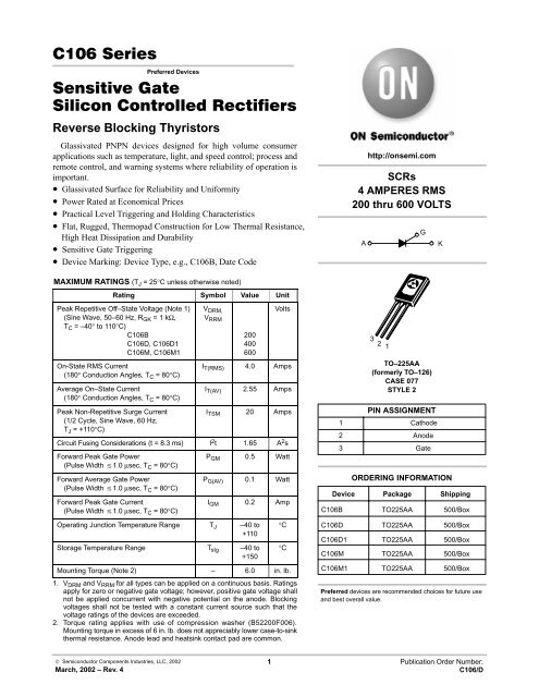
Preferred Devices<br />
<br />
<br />
Reverse Blocking Thyristors<br />
Glassivated PNPN devices designed for high volume consumer<br />
applications such as temperature, light, and speed control; process and<br />
remote control, and warning systems where reliability of operation is<br />
important.<br />
• Glassivated Surface for Reliability and Uniformity<br />
• Power Rated at Economical Prices<br />
• Practical Level Triggering and Holding Characteristics<br />
• Flat, Rugged, Thermopad Construction for Low Thermal Resistance,<br />
High Heat Dissipation and Durability<br />
• <strong>Sensitive</strong> <strong>Gate</strong> Triggering<br />
• Device Marking: Device Type, e.g., <strong>C106</strong>B, Date Code<br />
MAXIMUM RATINGS (T J = 25°C unless otherwise noted)<br />
Rating Symbol Value Unit<br />
Peak Repetitive Off–State Voltage (Note 1)<br />
(Sine Wave, 50–60 Hz, R GK = 1 kΩ,<br />
T C = –40° to 110°C)<br />
<strong>C106</strong>B<br />
<strong>C106</strong>D, <strong>C106</strong>D1<br />
<strong>C106</strong>M, <strong>C106</strong>M1<br />
On-State RMS Current<br />
(180° Conduction Angles, T C = 80°C)<br />
Average On–State Current<br />
(180° Conduction Angles, T C = 80°C)<br />
Peak Non-Repetitive Surge Current<br />
(1/2 Cycle, Sine Wave, 60 Hz,<br />
T J = +110°C)<br />
V DRM,<br />
V RRM<br />
200<br />
400<br />
600<br />
Volts<br />
I T(RMS) 4.0 Amps<br />
I T(AV) 2.55 Amps<br />
I TSM 20 Amps<br />
Circuit Fusing Considerations (t = 8.3 ms) I 2 t 1.65 A 2 s<br />
Forward Peak <strong>Gate</strong> Power<br />
(Pulse Width 1.0 µsec, T C = 80°C)<br />
Forward Average <strong>Gate</strong> Power<br />
(Pulse Width 1.0 µsec, T C = 80°C)<br />
Forward Peak <strong>Gate</strong> Current<br />
(Pulse Width 1.0 µsec, T C = 80°C)<br />
P GM 0.5 Watt<br />
P G(AV) 0.1 Watt<br />
I GM 0.2 Amp<br />
Operating Junction Temperature Range T J –40 to<br />
+110<br />
Storage Temperature Range T stg –40 to<br />
+150<br />
Mounting Torque (Note 2) – 6.0 in. lb.<br />
1. V DRM and V RRM for all types can be applied on a continuous basis. Ratings<br />
apply for zero or negative gate voltage; however, positive gate voltage shall<br />
not be applied concurrent with negative potential on the anode. Blocking<br />
voltages shall not be tested with a constant current source such that the<br />
voltage ratings of the devices are exceeded.<br />
2. Torque rating applies with use of compression washer (B52200F006).<br />
Mounting torque in excess of 6 in. lb. does not appreciably lower case-to-sink<br />
thermal resistance. Anode lead and heatsink contact pad are common.<br />
°C<br />
°C<br />
1<br />
2<br />
3<br />
SCRs<br />
4 AMPERES RMS<br />
200 thru 600 VOLTS<br />
A<br />
http://onsemi.com<br />
3<br />
2<br />
1<br />
ORDERING INFORMATION<br />
Device Package Shipping<br />
<strong>C106</strong>B TO225AA 500/Box<br />
<strong>C106</strong>D TO225AA 500/Box<br />
G<br />
TO–225AA<br />
(formerly TO–126)<br />
CASE 077<br />
STYLE 2<br />
PIN ASSIGNMENT<br />
Cathode<br />
Anode<br />
<strong>Gate</strong><br />
<strong>C106</strong>D1 TO225AA 500/Box<br />
<strong>C106</strong>M TO225AA 500/Box<br />
<strong>C106</strong>M1 TO225AA 500/Box<br />
Preferred devices are recommended choices for future use<br />
and best overall value.<br />
K<br />
© Semiconductor Components Industries, LLC, 2002<br />
March, 2002 – Rev. 4<br />
1 Publication Order Number:<br />
<strong>C106</strong>/D
<strong>C106</strong> <strong>Series</strong><br />
THERMAL CHARACTERISTICS (T C = 25°C unless otherwise noted.)<br />
Characteristic Symbol Max Unit<br />
Thermal Resistance, Junction to Case R θJC 3.0 °C/W<br />
Thermal Resistance, Junction to Ambient R θJA 75 °C/W<br />
Maximum Lead Temperature for Soldering Purposes 1/8″ from Case for 10 Seconds T L 260 °C<br />
ELECTRICAL CHARACTERISTICS (T C = 25°C unless otherwise noted.)<br />
Characteristic Symbol Min Typ Max Unit<br />
OFF CHARACTERISTICS<br />
Peak Repetitive Forward or Reverse Blocking Current<br />
(V AK = Rated V DRM or V RRM , R GK = 1000 Ohms) T J = 25°C<br />
T J = 110°C<br />
ON CHARACTERISTICS<br />
Peak Forward On–State Voltage (Note 3)<br />
(I TM = 4 A)<br />
<strong>Gate</strong> Trigger Current (Continuous dc) (Note 4)<br />
(V AK = 6 Vdc, R L = 100 Ohms) T J = 25°C<br />
T J = –40°C<br />
I DRM , I RRM<br />
–<br />
–<br />
–<br />
–<br />
10<br />
100<br />
µA<br />
µA<br />
V TM – – 2.2 Volts<br />
I GT<br />
–<br />
–<br />
Peak Reverse <strong>Gate</strong> Voltage (I GR = 10 µA) V GRM – – 6.0 Volts<br />
<strong>Gate</strong> Trigger Voltage (Continuous dc) (Note 4)<br />
(V AK = 6 Vdc, R L = 100 Ohms) T J = 25°C<br />
T J = –40°C<br />
<strong>Gate</strong> Non–Trigger Voltage (Continuous dc) (Note 4)<br />
(V AK = 12 V, R L = 100 Ohms, T J = 110°C)<br />
Latching Current<br />
(V AK = 12 V, I G = 20 mA) T J = 25°C<br />
T J = –40°C<br />
Holding Current (V D = 12 Vdc)<br />
(Initiating Current = 20 mA, <strong>Gate</strong> Open) T J = 25°C<br />
T J = –40°C<br />
T J = +110°C<br />
DYNAMIC CHARACTERISTICS<br />
Critical Rate–of–Rise of Off–State Voltage<br />
(V AK = Rated V DRM , Exponential Waveform, R GK = 1000 Ohms,<br />
T J = 110°C)<br />
3. Pulse Test: Pulse Width ≤ 2.0 ms, Duty Cycle ≤ 2%.<br />
4. R GK is not included in measurement.<br />
V GT<br />
0.4<br />
0.5<br />
15<br />
35<br />
0.60<br />
0.75<br />
200<br />
500<br />
0.8<br />
1.0<br />
µA<br />
Volts<br />
V GD 0.2 – – Volts<br />
I L<br />
–<br />
–<br />
I H<br />
–<br />
–<br />
–<br />
0.20<br />
0.35<br />
0.19<br />
0.33<br />
0.07<br />
5.0<br />
7.0<br />
3.0<br />
6.0<br />
2.0<br />
mA<br />
mA<br />
dv/dt – 8.0 – V/µs<br />
http://onsemi.com<br />
2
<strong>C106</strong> <strong>Series</strong><br />
Voltage Current Characteristic of SCR<br />
+ Current<br />
Anode +<br />
Symbol<br />
V DRM<br />
I DRM<br />
V RRM<br />
I RRM<br />
V TM<br />
I H<br />
Parameter<br />
Peak Repetitive Off State Forward Voltage<br />
Peak Forward Blocking Current<br />
Peak Repetitive Off State Reverse Voltage<br />
Peak Reverse Blocking Current<br />
Peak On State Voltage<br />
Holding Current<br />
I RRM at V RRM<br />
on state<br />
Reverse Blocking Region<br />
(off state)<br />
Reverse Avalanche Region<br />
V TM<br />
I H<br />
+ Voltage<br />
I DRM at V DRM<br />
Forward Blocking Region<br />
(off state)<br />
Anode –<br />
<br />
°<br />
<br />
<br />
<br />
<br />
<br />
<br />
<br />
<br />
<br />
<br />
<br />
<br />
<br />
<br />
<br />
<br />
<br />
Figure 1. Average Current Derating<br />
<br />
<br />
<br />
<br />
<br />
<br />
<br />
<br />
<br />
<br />
<br />
<br />
<br />
<br />
š<br />
<br />
<br />
Figure 2. Maximum On–State Power Dissipation<br />
<br />
http://onsemi.com<br />
3
<strong>C106</strong> <strong>Series</strong><br />
<br />
<br />
<br />
<br />
<br />
<br />
<br />
<br />
<br />
<br />
<br />
<br />
<br />
<br />
°<br />
°<br />
Figure 3. Typical <strong>Gate</strong> Trigger Current versus<br />
Junction Temperature<br />
Figure 4. Typical Holding Current versus<br />
Junction Temperature<br />
<br />
<br />
<br />
<br />
<br />
<br />
<br />
<br />
<br />
<br />
<br />
<br />
<br />
<br />
<br />
°<br />
<br />
<br />
<br />
<br />
°<br />
<br />
<br />
Figure 5. Typical <strong>Gate</strong> Trigger Voltage versus<br />
Junction Temperature<br />
Figure 6. Typical Latching Current versus<br />
Junction Temperature<br />
http://onsemi.com<br />
4
<strong>C106</strong> <strong>Series</strong><br />
Package Interchangeability<br />
The dimensional diagrams below compare the critical dimensions of the ON Semiconductor<br />
C-106 package with competitive devices. It has been demonstrated that the smaller dimensions of<br />
the ON Semiconductor package make it compatible in most lead-mount and chassis-mount<br />
applications. The user is advised to compare all critical dimensions for mounting compatibility.<br />
<br />
<br />
<br />
<br />
<br />
<br />
<br />
<br />
<br />
<br />
<br />
<br />
<br />
<br />
<br />
<br />
<br />
<br />
<br />
<br />
<br />
<br />
<br />
<br />
<br />
<br />
<br />
<br />
<br />
<br />
<br />
<br />
<br />
<br />
<br />
<br />
<br />
<br />
<br />
<br />
<br />
<br />
<br />
<br />
<br />
<br />
<br />
<br />
<br />
<br />
<br />
<br />
ON Semiconductor C-106 Package<br />
Competitive C-106 Package<br />
http://onsemi.com<br />
5
<strong>C106</strong> <strong>Series</strong><br />
PACKAGE DIMENSIONS<br />
TO–225AA<br />
(formerly TO–126)<br />
CASE 077–09<br />
ISSUE W<br />
H<br />
Q<br />
–B–<br />
U<br />
<br />
<br />
<br />
F<br />
–A–<br />
K<br />
V<br />
G<br />
S<br />
D 2 PL<br />
M<br />
<br />
<br />
<br />
<br />
C<br />
J<br />
R<br />
<br />
<br />
<br />
<br />
<br />
<br />
<br />
<br />
<br />
<br />
<br />
<br />
<br />
<br />
<br />
<br />
<br />
<br />
<br />
<br />
<br />
<br />
<br />
<br />
<br />
<br />
<br />
<br />
http://onsemi.com<br />
6
<strong>C106</strong> <strong>Series</strong><br />
Notes<br />
http://onsemi.com<br />
7
<strong>C106</strong> <strong>Series</strong><br />
ON Semiconductor is a trademark and is a registered trademark of Semiconductor Components Industries, LLC (SCILLC). SCILLC reserves the right<br />
to make changes without further notice to any products herein. SCILLC makes no warranty, representation or guarantee regarding the suitability of its products<br />
for any particular purpose, nor does SCILLC assume any liability arising out of the application or use of any product or circuit, and specifically disclaims any<br />
and all liability, including without limitation special, consequential or incidental damages. “Typical” parameters which may be provided in SCILLC data sheets<br />
and/or specifications can and do vary in different applications and actual performance may vary over time. All operating parameters, including “Typicals” must<br />
be validated for each customer application by customer’s technical experts. SCILLC does not convey any license under its patent rights nor the rights of others.<br />
SCILLC products are not designed, intended, or authorized for use as components in systems intended for surgical implant into the body, or other applications<br />
intended to support or sustain life, or for any other application in which the failure of the SCILLC product could create a situation where personal injury or death<br />
may occur. Should Buyer purchase or use SCILLC products for any such unintended or unauthorized application, Buyer shall indemnify and hold SCILLC<br />
and its officers, employees, subsidiaries, affiliates, and distributors harmless against all claims, costs, damages, and expenses, and reasonable attorney fees<br />
arising out of, directly or indirectly, any claim of personal injury or death associated with such unintended or unauthorized use, even if such claim alleges that<br />
SCILLC was negligent regarding the design or manufacture of the part. SCILLC is an Equal Opportunity/Affirmative Action Employer.<br />
PUBLICATION ORDERING INFORMATION<br />
Literature Fulfillment:<br />
Literature Distribution Center for ON Semiconductor<br />
P.O. Box 5163, Denver, Colorado 80217 USA<br />
Phone: 303–675–2175 or 800–344–3860 Toll Free USA/Canada<br />
Fax: 303–675–2176 or 800–344–3867 Toll Free USA/Canada<br />
Email: ONlit@hibbertco.com<br />
N. American Technical Support: 800–282–9855 Toll Free USA/Canada<br />
JAPAN: ON Semiconductor, Japan Customer Focus Center<br />
4–32–1 Nishi–Gotanda, Shinagawa–ku, Tokyo, Japan 141–0031<br />
Phone: 81–3–5740–2700<br />
Email: r14525@onsemi.com<br />
ON Semiconductor Website: http://onsemi.com<br />
For additional information, please contact your local<br />
Sales Representative.<br />
http://onsemi.com<br />
8<br />
<strong>C106</strong>/D