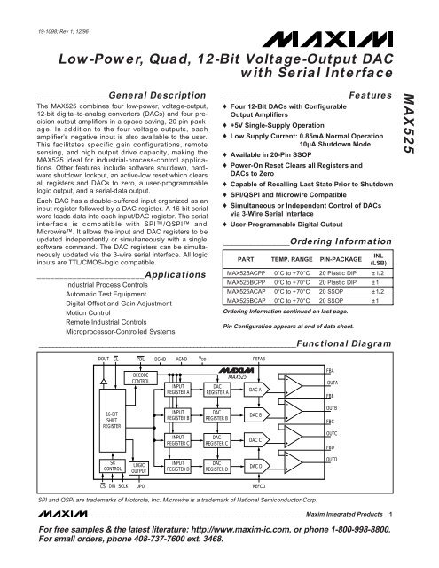
MAX525 Low-Power, Quad, 12-Bit Voltage-Output ... - Micro/sys, Inc.
MAX525 Low-Power, Quad, 12-Bit Voltage-Output ... - Micro/sys, Inc.
MAX525 Low-Power, Quad, 12-Bit Voltage-Output ... - Micro/sys, Inc.

You also want an ePaper? Increase the reach of your titles
YUMPU automatically turns print PDFs into web optimized ePapers that Google loves.
19-1098; Rev 1; <strong>12</strong>/96<br />
<strong>Low</strong>-<strong>Power</strong>, <strong>Quad</strong>, <strong>12</strong>-<strong>Bit</strong> <strong>Voltage</strong>-<strong>Output</strong> DAC<br />
with Serial Interface<br />
__________________General Description<br />
The <strong>MAX525</strong> combines four low-power, voltage-output,<br />
<strong>12</strong>-bit digital-to-analog converters (DACs) and four precision<br />
output amplifiers in a space-saving, 20-pin package.<br />
In addition to the four voltage outputs, each<br />
amplifier’s negative input is also available to the user.<br />
This facilitates specific gain configurations, remote<br />
sensing, and high output drive capacity, making the<br />
<strong>MAX525</strong> ideal for industrial-process-control applications.<br />
Other features include software shutdown, hardware<br />
shutdown lockout, an active-low reset which clears<br />
all registers and DACs to zero, a user-programmable<br />
logic output, and a serial-data output.<br />
Each DAC has a double-buffered input organized as an<br />
input register followed by a DAC register. A 16-bit serial<br />
word loads data into each input/DAC register. The serial<br />
interface is compatible with SPI/QSPI and<br />
<strong>Micro</strong>wire. It allows the input and DAC registers to be<br />
updated independently or simultaneously with a single<br />
software command. The DAC registers can be simultaneously<br />
updated via the 3-wire serial interface. All logic<br />
inputs are TTL/CMOS-logic compatible.<br />
________________________Applications<br />
Industrial Process Controls<br />
Automatic Test Equipment<br />
Digital Offset and Gain Adjustment<br />
Motion Control<br />
Remote Industrial Controls<br />
<strong>Micro</strong>processor-Controlled Systems<br />
______________________________Features<br />
♦ Four <strong>12</strong>-<strong>Bit</strong> DACs with Configurable<br />
<strong>Output</strong> Amplifiers<br />
♦ +5V Single-Supply Operation<br />
♦ <strong>Low</strong> Supply Current: 0.85mA Normal Operation<br />
10µA Shutdown Mode<br />
♦ Available in 20-Pin SSOP<br />
♦ <strong>Power</strong>-On Reset Clears all Registers and<br />
DACs to Zero<br />
♦ Capable of Recalling Last State Prior to Shutdown<br />
♦ SPI/QSPI and <strong>Micro</strong>wire Compatible<br />
♦ Simultaneous or Independent Control of DACs<br />
via 3-Wire Serial Interface<br />
♦ User-Programmable Digital <strong>Output</strong><br />
_________________Ordering Information<br />
_________________________________________________________________________Functional Diagram<br />
PART<br />
<strong>MAX525</strong>ACPP<br />
<strong>MAX525</strong>BCPP<br />
<strong>MAX525</strong>ACAP<br />
<strong>MAX525</strong>BCAP<br />
TEMP. RANGE<br />
PIN-PACKAGE<br />
0°C to +70°C 20 Plastic DIP<br />
0°C to +70°C 20 Plastic DIP<br />
0°C to +70°C 20 SSOP<br />
0°C to +70°C 20 SSOP<br />
Ordering Information continued on last page.<br />
Pin Configuration appears at end of data sheet.<br />
INL<br />
(LSB)<br />
±1/2<br />
±1<br />
±1/2<br />
±1<br />
<strong>MAX525</strong><br />
DOUT<br />
CL<br />
PDL<br />
DGND<br />
AGND<br />
V DD<br />
REFAB<br />
DECODE<br />
CONTROL<br />
INPUT<br />
REGISTER A<br />
DAC<br />
REGISTER A<br />
<strong>MAX525</strong><br />
DAC A<br />
FBA<br />
OUTA<br />
FBB<br />
16-BIT<br />
SHIFT<br />
REGISTER<br />
INPUT<br />
REGISTER B<br />
INPUT<br />
REGISTER C<br />
DAC<br />
REGISTER B<br />
DAC<br />
REGISTER C<br />
DAC B<br />
DAC C<br />
OUTB<br />
FBC<br />
OUTC<br />
FBD<br />
SR<br />
CONTROL<br />
LOGIC<br />
OUTPUT<br />
INPUT<br />
REGISTER D<br />
DAC<br />
REGISTER D<br />
DAC D<br />
OUTD<br />
CS<br />
DIN SCLK<br />
UPO<br />
REFCD<br />
SPI and QSPI are trademarks of Motorola, <strong>Inc</strong>. <strong>Micro</strong>wire is a trademark of National Semiconductor Corp.<br />
________________________________________________________________ Maxim Integrated Products 1<br />
For free samples & the latest literature: http://www.maxim-ic.com, or phone 1-800-998-8800.<br />
For small orders, phone 408-737-7600 ext. 3468.
<strong>Low</strong>-<strong>Power</strong>, <strong>Quad</strong>, <strong>12</strong>-<strong>Bit</strong> <strong>Voltage</strong>-<strong>Output</strong> DAC<br />
with Serial Interface<br />
<strong>MAX525</strong><br />
ABSOLUTE MAXIMUM RATINGS<br />
V DD to AGND............................................................-0.3V to +6V<br />
V DD to DGND ...........................................................-0.3V to +6V<br />
AGND to DGND ..................................................................±0.3V<br />
REFAB, REFCD to AGND...........................-0.3V to (V DD + 0.3V)<br />
OUT_, FB_ to AGND...................................-0.3V to (V DD + 0.3V)<br />
Digital Inputs to DGND.............................................-0.3V to +6V<br />
DOUT, UPO to DGND ................................-0.3V to (V DD + 0.3V)<br />
Continuous Current into Any Pin.......................................±20mA<br />
Continuous <strong>Power</strong> Dissipation (T A = +70°C)<br />
Plastic DIP (derate 8.00mW/°C above +70°C) .................640mW<br />
SSOP (derate 8.00mW/°C above +70°C) ......................640mW<br />
CERDIP (derate 11.11mW/°C above +70°C).................889mW<br />
Operating Temperature Ranges<br />
<strong>MAX525</strong>_C_P ........................................................0°C to +70°C<br />
<strong>MAX525</strong>_E_P .....................................................-40°C to +85°C<br />
<strong>MAX525</strong>_MJP ..................................................-55°C to +<strong>12</strong>5°C<br />
Storage Temperature Range .............................-65°C to +150°C<br />
Lead Temperature (soldering, 10sec) .............................+300°C<br />
Stresses beyond those listed under “Absolute Maximum Ratings” may cause permanent damage to the device. These are stress ratings only, and functional<br />
operation of the device at these or any other conditions beyond those indicated in the operational sections of the specifications is not implied. Exposure to<br />
absolute maximum rating conditions for extended periods may affect device reliability.<br />
ELECTRICAL CHARACTERISTICS<br />
(V DD = +5V ±10%, AGND = DGND = 0V, REFAB = REFCD = 2.5V, R L = 5kΩ, C L = 100pF, T A = T MIN to T MAX , unless otherwise<br />
noted. Typical values are at T A = +25°C. <strong>Output</strong> buffer connected in unity-gain configuration (Figure 9).)<br />
Resolution<br />
Integral Nonlinearity<br />
(Note 1)<br />
Differential Nonlinearity<br />
Offset Error<br />
CONDITIONS<br />
Guaranteed monotonic<br />
<strong>Power</strong>-Supply Rejection Ratio PSRR 4.5V ≤ V DD ≤ 5.5V<br />
100 600<br />
Gain Error<br />
PARAMETER<br />
Offset-Error Tempco<br />
Gain-Error Tempco<br />
Integral Nonlinearity<br />
Reference Input Range<br />
Reference Input Resistance<br />
SYMBOL<br />
STATIC PERFORMANCE—ANALOG SECTION<br />
N<br />
INL<br />
DNL<br />
V OS<br />
GE<br />
Offset Error ±1.0 ±6.0<br />
INL<br />
V REF<br />
R REF<br />
Code-dependent, minimum at code 555 hex<br />
<strong>12</strong><br />
0 V DD - 1.4<br />
10<br />
±0.25 ±0.5<br />
Gain Error (Note 1) GE<br />
-0.8 ±2.0<br />
MATCHING PERFORMANCE (T A = +25°C)<br />
REFERENCE INPUT<br />
Reference Current in Shutdown<br />
<strong>MAX525</strong>A<br />
<strong>MAX525</strong>B<br />
MIN TYP MAX<br />
6<br />
1<br />
±1.0<br />
±1.0<br />
-0.8 ±2.0<br />
±0.35 ±1.0<br />
0.01 ±1<br />
UNITS<br />
<strong>Bit</strong>s<br />
LSB<br />
LSB<br />
±6.0 mV<br />
ppm/°C<br />
LSB<br />
ppm/°C<br />
µV/V<br />
LSB<br />
mV<br />
LSB<br />
V<br />
kΩ<br />
µA<br />
2 _______________________________________________________________________________________
<strong>Low</strong>-<strong>Power</strong>, <strong>Quad</strong>, <strong>12</strong>-<strong>Bit</strong> <strong>Voltage</strong>-<strong>Output</strong> DAC<br />
with Serial Interface<br />
ELECTRICAL CHARACTERISTICS (continued)<br />
(V DD = +5V ±10%, AGND = DGND = 0V, REFAB = REFCD = 2.5V, R L = 5kΩ, C L = 100pF, T A = T MIN to T MAX , unless otherwise<br />
noted. Typical values are at T A = +25°C. <strong>Output</strong> buffer connected in unity-gain configuration (Figure 9).)<br />
PARAMETER SYMBOL<br />
MULTIPLYING-MODE PERFORMANCE<br />
Reference -3dB Bandwidth<br />
Reference Feedthrough<br />
Signal-to-Noise Plus<br />
Distortion Ratio<br />
DIGITAL INPUTS<br />
Input High <strong>Voltage</strong><br />
Input <strong>Low</strong> <strong>Voltage</strong><br />
Input Leakage Current<br />
Input Capacitance<br />
DIGITAL OUTPUTS<br />
<strong>Output</strong> High <strong>Voltage</strong><br />
<strong>Output</strong> <strong>Low</strong> <strong>Voltage</strong><br />
DYNAMIC PERFORMANCE<br />
<strong>Voltage</strong> <strong>Output</strong> Slew Rate<br />
<strong>Output</strong> Settling Time<br />
<strong>Output</strong> <strong>Voltage</strong> Swing<br />
Current into FB_<br />
OUT_ Leakage Current<br />
in Shutdown<br />
Start-Up Time Exiting<br />
Shutdown Mode<br />
SINAD<br />
V IH<br />
V IL<br />
I IN<br />
C IN<br />
V OH<br />
V OL<br />
SR<br />
V REF = 0.67Vp-p<br />
V REF = 1Vp-p at 25kHz<br />
V IN = 0V or V DD<br />
I SOURCE = 2mA<br />
I SINK = 2mA<br />
To ±1/2LSB, V STEP = 2.5V<br />
Rail to rail (Note 2)<br />
CONDITIONS<br />
Input code = all 0s, V REF = 3.6Vp-p at 1kHz<br />
MIN TYP MAX<br />
2.4<br />
V DD - 0.5<br />
650<br />
72<br />
0.01 ±1.0<br />
8<br />
0.13 0.4<br />
0.6<br />
<strong>12</strong><br />
0 to V DD<br />
0 0.1<br />
15<br />
0.8<br />
UNITS<br />
R L = ∞ 0.01 ±1 µA<br />
-84<br />
kHz<br />
dB<br />
dB<br />
V<br />
V<br />
µA<br />
pF<br />
V<br />
V<br />
V/µs<br />
µs<br />
V<br />
µA<br />
µs<br />
<strong>MAX525</strong><br />
Digital Feedthrough<br />
Digital Crosstalk<br />
POWER SUPPLIES<br />
Supply <strong>Voltage</strong><br />
Supply Current<br />
Supply Current in Shutdown<br />
Reference Current in Shutdown<br />
V DD<br />
I DD<br />
CS = V DD , DIN = 100kHz<br />
(Note 3)<br />
5<br />
5<br />
4.5 5.5<br />
0.85 0.98<br />
(Note 3) 10 20 µA<br />
0.01 ±1<br />
nV-s<br />
nV-s<br />
V<br />
mA<br />
µA<br />
Note 1: Guaranteed from code 11 to code 4095 in unity-gain configuration.<br />
Note 2: Accuracy is better than 1.0LSB for V OUT = 6mV to V DD - 60mV, guaranteed by PSR test on end points.<br />
Note 3: R L = ∞, digital inputs at DGND or V DD .<br />
_______________________________________________________________________________________ 3
<strong>Low</strong>-<strong>Power</strong>, <strong>Quad</strong>, <strong>12</strong>-<strong>Bit</strong> <strong>Voltage</strong>-<strong>Output</strong> DAC<br />
with Serial Interface<br />
<strong>MAX525</strong><br />
ELECTRICAL CHARACTERISTICS (continued)<br />
(V DD = +5V ±10%, AGND = DGND = 0V, REFAB = REFCD = 2.5V, R L = 5kΩ, C L = 100pF, T A = T MIN to T MAX , unless otherwise<br />
noted. Typical values are at T A = +25°C. <strong>Output</strong> buffer connected in unity-gain configuration (Figure 9).)<br />
PARAMETER SYMBOL<br />
TIMING CHARACTERISTICS (Figure 6)<br />
SCLK Clock Period<br />
t CP<br />
SCLK Pulse Width High<br />
SCLK Pulse Width <strong>Low</strong><br />
CS Fall to SCLK Rise Setup Time<br />
SCLK Rise to CS Rise Hold Time<br />
DIN Setup Time<br />
DIN Hold Time<br />
SCLK Rise to DOUT Valid<br />
Propagation Delay<br />
SCLK Fall to DOUT Valid<br />
Propagation Delay<br />
SCLK Rise to CS Fall Delay<br />
CS Rise to SCLK Rise Hold Time<br />
CS Pulse Width High<br />
t CH<br />
t CL<br />
t CSS<br />
t CSH<br />
t DS<br />
t DH<br />
t D01<br />
t D02<br />
t CS0<br />
t CS1<br />
t CSW<br />
C LOAD = 200pF<br />
C LOAD = 200pF<br />
CONDITIONS<br />
MIN TYP MAX<br />
100<br />
40<br />
40<br />
40<br />
0<br />
40<br />
0<br />
40<br />
40<br />
100<br />
80<br />
70<br />
80<br />
UNITS<br />
ns<br />
ns<br />
ns<br />
ns<br />
ns<br />
ns<br />
ns<br />
ns<br />
ns<br />
ns<br />
ns<br />
ns<br />
__________________________________________Typical Operating Characteristics<br />
(V DD = +5V, T A = +25°C, unless otherwise noted.)<br />
INL (LSB)<br />
0.3<br />
0.2<br />
0.1<br />
0<br />
-0.1<br />
-0.2<br />
-0.3<br />
INTEGRAL NONLINEARITY<br />
vs. REFERENCE VOLTAGE<br />
-0.4<br />
R L = 5kΩ<br />
-0.5<br />
0.4 0.8 1.2 1.6 2.0 2.4 2.8 3.2 3.6 4.0<br />
REFERENCE VOLTAGE (V)<br />
<strong>MAX525</strong>-01<br />
4.4<br />
RELATIVE OUTPUT (dB)<br />
0<br />
-4<br />
-8<br />
-<strong>12</strong><br />
-16<br />
REFERENCE VOLTAGE INPUT<br />
FREQUENCY RESPONSE<br />
REFAB SWEPT 0.67Vp-p<br />
R L = 5kΩ<br />
C L = 100pF<br />
-20<br />
0 500k 1M 1.5M 2M 2.5M 3M<br />
FREQUENCY (Hz)<br />
<strong>MAX525</strong>-02<br />
SUPPLY CURRENT (µA)<br />
SUPPLY CURRENT<br />
vs. TEMPERATURE<br />
1000<br />
950<br />
900<br />
850<br />
800<br />
750<br />
700<br />
650<br />
600<br />
CODE = FFF hex<br />
550<br />
500<br />
-55 -40 -20 0 20 40 60 80 100 <strong>12</strong>0<br />
TEMPERATURE (°C)<br />
<strong>MAX525</strong>-03<br />
4 _______________________________________________________________________________________
<strong>Low</strong>-<strong>Power</strong>, <strong>Quad</strong>, <strong>12</strong>-<strong>Bit</strong> <strong>Voltage</strong>-<strong>Output</strong> DAC<br />
with Serial Interface<br />
____________________________Typical Operating Characteristics (continued)<br />
(V DD = +5V, T A = +25°C, unless otherwise noted.)<br />
SUPPLY CURRENT (µA)<br />
1000<br />
950<br />
900<br />
850<br />
800<br />
750<br />
700<br />
SUPPLY CURRENT<br />
vs. SUPPLY VOLTAGE<br />
650<br />
CODE = FFF hex<br />
600<br />
4.0 4.2 4.4 4.6 4.8 5.0 5.2 5.4 5.6<br />
SUPPLY VOLTAGE (V)<br />
<strong>MAX525</strong>-04<br />
THD + NOISE (%)<br />
TOTAL HARMONIC DISTORTION PLUS NOISE<br />
vs. FREQUENCY<br />
0.50<br />
DAC CODE = ALL 1s<br />
0.45<br />
REFAB = 1Vp-p<br />
0.40 R L = 5kΩ<br />
C L = 100pF<br />
0.35<br />
0.30<br />
0.25<br />
0.20<br />
0.15<br />
0.10<br />
0.05<br />
0<br />
1 10<br />
100<br />
FREQUENCY (kHz)<br />
<strong>MAX525</strong>-05<br />
SIGNAL AMPLITUDE (dB)<br />
0<br />
-20<br />
-40<br />
-60<br />
-80<br />
OUTPUT FFT PLOT<br />
V REF = 1kHz, 0.006V TO 3.6V<br />
R L = 5kΩ<br />
C L = 100pF<br />
-100<br />
0.5 1.6 2.7 3.8 4.9 6.0<br />
FREQUENCY (kHz)<br />
<strong>MAX525</strong>-10<br />
<strong>MAX525</strong><br />
0<br />
FULL-SCALE ERROR<br />
vs. LOAD<br />
<strong>MAX525</strong>-09<br />
0<br />
REFERENCE FEEDTHROUGH<br />
AT 1kHz<br />
REFAB INPUT SIGNAL<br />
<strong>MAX525</strong>-11<br />
FULL-SCALE ERROR (LSB)<br />
-1<br />
-2<br />
-3<br />
-4<br />
SIGNAL AMPLITUDE (dB)<br />
-20<br />
-40<br />
-60<br />
-80<br />
V REF = 3.6Vp-p @ 1kHz<br />
R L = 5kΩ<br />
C L = 100pF<br />
OUTA FEEDTHROUGH<br />
-5<br />
0.01 0.1 1 10 100<br />
LOAD (kΩ)<br />
-100<br />
0.5 1.2 1.9 2.6 3.3 4.0<br />
FREQUENCY (kHz)<br />
_______________________________________________________________________________________ 5
<strong>Low</strong>-<strong>Power</strong>, <strong>Quad</strong>, <strong>12</strong>-<strong>Bit</strong> <strong>Voltage</strong>-<strong>Output</strong> DAC<br />
with Serial Interface<br />
<strong>MAX525</strong><br />
____________________________Typical Operating Characteristics (continued)<br />
(V DD = +5V, T A = +25°C, unless otherwise noted.)<br />
MAJOR-CARRY TRANSITION<br />
DIGITAL FEEDTHROUGH (SCLK = 100kHz)<br />
<strong>MAX525</strong>-07<br />
CS<br />
5V/div<br />
<strong>MAX525</strong>-08<br />
SCLK,<br />
2V/div<br />
OUTB,<br />
AC COUPLED<br />
100mV/div<br />
OUTA,<br />
AC COUPLED<br />
10mV/div<br />
10µs/div<br />
V REF = 2.5V, R L = 5kΩ, C L = 100pF<br />
CS = PDL = CL = 5V, DIN = 0V<br />
DAC A CODE SET TO 800 hex<br />
2µs/div<br />
V REF = 2.5V, R L = 5kΩ, CL = 100pF<br />
ANALOG CROSSTALK<br />
DYNAMIC RESPONSE<br />
<strong>MAX525</strong>-<strong>12</strong><br />
OUTA,<br />
1V/div<br />
<strong>MAX525</strong>-13<br />
OUTA,<br />
1V/div<br />
GND<br />
OUTB,<br />
AC COUPLED<br />
10mV/div<br />
10µs/div<br />
V REF = 2.5V, R L = 5kΩ, C L = 100pF<br />
DAC A CODE SWITCHING FROM 00B hex TO FFF hex<br />
DAC B CODE SET TO 800 hex<br />
10µs/div<br />
V REF = 2.5V, R L = 5kΩ, C L = 100pF<br />
SWITCHING FROM CODE 000 hex TO FB4 hex<br />
OUTPUT AMPLIFIER GAIN = +2<br />
6 _______________________________________________________________________________________
<strong>Low</strong>-<strong>Power</strong>, <strong>Quad</strong>, <strong>12</strong>-<strong>Bit</strong> <strong>Voltage</strong>-<strong>Output</strong> DAC<br />
with Serial Interface<br />
______________________________________________________________Pin Description<br />
PIN NAME<br />
FUNCTION<br />
1 AGND Analog Ground<br />
2 FBA DAC A <strong>Output</strong> Amplifier Feedback<br />
3 OUTA DAC A <strong>Output</strong> <strong>Voltage</strong><br />
<strong>MAX525</strong><br />
4<br />
5<br />
6<br />
7<br />
8<br />
9<br />
10<br />
11<br />
<strong>12</strong><br />
13<br />
14<br />
15<br />
16<br />
17<br />
18<br />
19<br />
20<br />
OUTB<br />
FBB<br />
REFAB<br />
CL<br />
CS<br />
DIN<br />
SCLK<br />
DGND<br />
DOUT<br />
UPO<br />
PDL<br />
REFCD<br />
FBC<br />
OUTC<br />
OUTD<br />
FBD<br />
V DD<br />
DAC B <strong>Output</strong> <strong>Voltage</strong><br />
DAC B <strong>Output</strong> Amplifier Feedback<br />
Reference <strong>Voltage</strong> Input for DAC A and DAC B<br />
Clear All DACs and Registers. Resets all outputs (OUT_, UPO, DOUT) to 0, active low.<br />
Chip-Select Input. Active low.<br />
Serial-Data Input<br />
Serial Clock Input<br />
Digital Ground<br />
Serial-Data <strong>Output</strong><br />
User-Programmable Logic <strong>Output</strong><br />
<strong>Power</strong>-Down Lockout. Active low. Locks out software shutdown if low.<br />
Reference <strong>Voltage</strong> Input for DAC C and DAC D<br />
DAC C <strong>Output</strong> Amplifier Feedback<br />
DAC C <strong>Output</strong> <strong>Voltage</strong><br />
DAC D <strong>Output</strong> <strong>Voltage</strong><br />
DAC D <strong>Output</strong> Amplifier Feedback<br />
Positive <strong>Power</strong> Supply<br />
_______________________________________________________________________________________ 7
<strong>Low</strong>-<strong>Power</strong>, <strong>Quad</strong>, <strong>12</strong>-<strong>Bit</strong> <strong>Voltage</strong>-<strong>Output</strong> DAC<br />
with Serial Interface<br />
<strong>MAX525</strong><br />
REF_<br />
AGND<br />
SHOWN FOR ALL 1s ON DAC<br />
R R R<br />
2R 2R 2R 2R 2R<br />
D0 D9 D10 D11<br />
Figure 1. Simplified DAC Circuit Diagram<br />
OUT_<br />
_______________Detailed Description<br />
The <strong>MAX525</strong> contains four <strong>12</strong>-bit, voltage-output digital-to-analog<br />
converters (DACs) that are easily<br />
addressed using a simple 3-wire serial interface. It<br />
includes a 16-bit data-in/data-out shift register, and<br />
each DAC has a doubled-buffered input composed of<br />
an input register and a DAC register (see Functional<br />
Diagram). In addition to the four voltage outputs, each<br />
amplifier’s negative input is available to the user.<br />
The DACs are inverted R-2R ladder networks that convert<br />
<strong>12</strong>-bit digital inputs into equivalent analog output<br />
voltages in proportion to the applied reference voltage<br />
inputs. DACs A and B share the REFAB reference input,<br />
while DACs C and D share the REFCD reference input.<br />
The two reference inputs allow different full-scale output<br />
voltage ranges for each pair of DACs. Figure 1 shows a<br />
simplified circuit diagram of one of the four DACs.<br />
Reference Inputs<br />
The two reference inputs accept positive DC and AC<br />
signals. The voltage at each reference input sets the<br />
full-scale output voltage for its two corresponding<br />
DACs. The reference input voltage range is 0V to (VDD<br />
- 1.4V). The output voltages (VOUT_) are represented by<br />
a digitally programmable voltage source as:<br />
VOUT_ = (VREF x NB / 4096) x Gain<br />
where NB is the numeric value of the DAC’s binary<br />
input code (0 to 4095), VREF is the reference voltage,<br />
and Gain is the externally set voltage gain.<br />
FB_<br />
The impedance at each reference input is code-dependent,<br />
ranging from a low value of 10kΩ when both<br />
DACs connected to the reference have an input code<br />
of 555 hex, to a high value exceeding several gigohms<br />
(leakage currents) with an input code of 000 hex.<br />
Because the input impedance at the reference pins is<br />
code-dependent, load regulation of the reference<br />
source is important.<br />
The REFAB and REFCD reference inputs have a 10kΩ<br />
guaranteed minimum input impedance. When the two<br />
reference inputs are driven from the same source, the<br />
effective minimum impedance is 5kΩ. A voltage reference<br />
with a load regulation of 6ppm/mA, such as the<br />
MAX873, would typically deviate by 0.025LSB<br />
(0.061LSB worst case) when driving both <strong>MAX525</strong> reference<br />
inputs simultaneously at 2.5V. Driving the<br />
REFAB and REFCD pins separately improves reference<br />
accuracy.<br />
In shutdown mode, the <strong>MAX525</strong>’s REFAB and REFCD<br />
inputs enter a high-impedance state with a typical input<br />
leakage current of 0.01µA.<br />
The reference input capacitance is also code dependent<br />
and typically ranges from 20pF with an input code<br />
of all 0s to 100pF with an input code of all 1s.<br />
<strong>Output</strong> Amplifiers<br />
All <strong>MAX525</strong> DAC outputs are internally buffered by precision<br />
amplifiers with a typical slew rate of 0.6V/µs. Access<br />
to the inverting input of each output amplifier provides<br />
the user greater flexibility in output gain setting/<br />
signal conditioning (see the Applications Information section).<br />
With a full-scale transition at the <strong>MAX525</strong> output, the<br />
typical settling time to ±1/2LSB is <strong>12</strong>µs when loaded<br />
with 5kΩ in parallel with 100pF (loads less than 2kΩ<br />
degrade performance).<br />
The <strong>MAX525</strong> output amplifier’s output dynamic responses<br />
and settling performances are shown in the Typical<br />
Operating Characteristics.<br />
<strong>Power</strong>-Down Mode<br />
The <strong>MAX525</strong> features a software-programmable shutdown<br />
that reduces supply current to a typical value of<br />
10µA. The power-down lockout (PDL) pin must be high to<br />
enable the shutdown mode. Writing 1100XXXXXXXXXXXX<br />
as the input-control word puts the <strong>MAX525</strong> in powerdown<br />
mode (Table 1).<br />
8 _______________________________________________________________________________________
<strong>Low</strong>-<strong>Power</strong>, <strong>Quad</strong>, <strong>12</strong>-<strong>Bit</strong> <strong>Voltage</strong>-<strong>Output</strong> DAC<br />
with Serial Interface<br />
In power-down mode, the <strong>MAX525</strong> output amplifiers<br />
and the reference inputs enter a high-impedance state.<br />
The serial interface remains active. Data in the input<br />
registers is retained in power-down, allowing the<br />
<strong>MAX525</strong> to recall the output states prior to entering<br />
shutdown. Start up from power-down either by recalling<br />
the previous configuration or by updating the DACs<br />
with new data. When powering up the device or bringing<br />
it out of shutdown, allow 15µs for the outputs to stabilize.<br />
Serial-Interface Configurations<br />
The <strong>MAX525</strong>’s 3-wire serial interface is compatible<br />
with both <strong>Micro</strong>wire (Figure 2) and SPI/QSPI<br />
(Figure 3). The serial input word consists of two address<br />
bits and two control bits followed by <strong>12</strong> data bits<br />
(MSB first), as shown in Figure 4. The 4-bit address/<br />
control code determines the <strong>MAX525</strong>’s response outlined<br />
in Table 1. The connection between DOUT and<br />
the serial-interface port is not necessary, but may be<br />
used for data echo. Data held in the <strong>MAX525</strong>’s shift<br />
register can be shifted out of DOUT and returned to the<br />
microprocessor (µP) for data verification.<br />
The <strong>MAX525</strong>’s digital inputs are double buffered.<br />
Depending on the command issued through the serial<br />
interface, the input register(s) can be loaded without<br />
affecting the DAC register(s), the DAC register(s) can<br />
be loaded directly, or all four DAC registers can be<br />
updated simultaneously from the input registers<br />
(Table 1).<br />
Serial-Interface Description<br />
The <strong>MAX525</strong> requires 16 bits of serial data. Table 1 lists<br />
the serial-interface programming commands. For certain<br />
commands, the <strong>12</strong> data bits are “don’t cares.” Data<br />
is sent MSB first and can be sent in two 8-bit packets or<br />
one 16-bit word (CS must remain low until 16 bits are<br />
transferred). The serial data is composed of two DAC<br />
address bits (A1, A0) and two control bits (C1, C0),<br />
followed by the <strong>12</strong> data bits D11…D0 (Figure 4). The<br />
4-bit address/control code determines:<br />
• The register(s) to be updated<br />
• The clock edge on which data is to be clocked out<br />
via the serial-data output (DOUT)<br />
• The state of the user-programmable logic output<br />
(UPO)<br />
• If the part is to go into shutdown mode (assuming<br />
PDL is high)<br />
• How the part is configured when coming out of shutdown<br />
mode.<br />
<strong>MAX525</strong><br />
SCLK<br />
DIN<br />
DOUT*<br />
CS<br />
SK<br />
SO<br />
SI*<br />
I/O<br />
MICROWIRE<br />
PORT<br />
*THE DOUT-SI CONNECTION IS NOT REQUIRED FOR WRITING TO THE <strong>MAX525</strong>,<br />
BUT MAY BE USED FOR READBACK PURPOSES.<br />
Figure 2. Connections for <strong>Micro</strong>wire<br />
<strong>MAX525</strong><br />
DOUT*<br />
DIN<br />
SCLK<br />
CS<br />
MISO*<br />
MOSI<br />
SCK<br />
I/O<br />
+5V<br />
SS<br />
SPI/QSPI<br />
PORT<br />
CPOL = 0, CPHA = 0<br />
*THE DOUT-MISO CONNECTION IS NOT REQUIRED FOR WRITING TO THE <strong>MAX525</strong>,<br />
BUT MAY BE USED FOR READBACK PURPOSES.<br />
Figure 3. Connections for SPI/QSPI<br />
MSB ..................................................................................LSB<br />
Address<br />
<strong>Bit</strong>s<br />
Control<br />
<strong>Bit</strong>s<br />
Figure 4. Serial-Data Format<br />
16 <strong>Bit</strong>s of Serial Data<br />
Data <strong>Bit</strong>s<br />
MSB.............................................LSB<br />
A1 A0 C1 C0 D11................................................D0<br />
4 Address/<br />
Control <strong>Bit</strong>s<br />
<strong>12</strong> Data <strong>Bit</strong>s<br />
<strong>MAX525</strong><br />
_______________________________________________________________________________________ 9
<strong>Low</strong>-<strong>Power</strong>, <strong>Quad</strong>, <strong>12</strong>-<strong>Bit</strong> <strong>Voltage</strong>-<strong>Output</strong> DAC<br />
with Serial Interface<br />
<strong>MAX525</strong><br />
Table 1. Serial-Interface Programming Commands<br />
C1<br />
16-BIT C0SERIAL WORD<br />
A1 A0 C1 C0<br />
0 0<br />
0 1<br />
1 0<br />
1 1<br />
0 1<br />
0 1<br />
0 1<br />
0 1<br />
D11.................D0<br />
MSB LSB<br />
<strong>12</strong>-bit DAC data<br />
<strong>12</strong>-bit DAC data<br />
<strong>12</strong>-bit DAC data<br />
<strong>12</strong>-bit DAC data<br />
FUNCTION<br />
Load input register A; DAC registers unchanged.<br />
Load input register B; DAC registers unchanged.<br />
Load input register C; DAC registers unchanged.<br />
Load input register D; DAC registers unchanged.<br />
0 0<br />
0 1<br />
1 0<br />
1 1<br />
1 1<br />
1 1<br />
1 1<br />
1 1<br />
<strong>12</strong>-bit DAC data<br />
<strong>12</strong>-bit DAC data<br />
<strong>12</strong>-bit DAC data<br />
<strong>12</strong>-bit DAC data<br />
Load input register A; all DAC registers updated.<br />
Load input register B; all DAC registers updated.<br />
Load input register C; all DAC registers updated.<br />
Load input register D; all DAC registers updated.<br />
0 1<br />
1 0 0 0 <strong>12</strong>-bit DAC data Load all DAC registers from shift register (start-up).<br />
1 1<br />
0 0<br />
0 1<br />
0 0<br />
0 0<br />
1 0<br />
1 0<br />
XXXXXXXXXXXX<br />
XXXXXXXXXXXX<br />
XXXXXXXXXXXX<br />
XXXXXXXXXXXX<br />
Update all DAC registers from their respective input registers (start-up).<br />
Shutdown (provided PDL = 1)<br />
UPO goes low (default)<br />
UPO goes high<br />
0 0 0 0 XXXXXXXXXXXX No operation (NOP) to DAC registers<br />
1 1<br />
1 0<br />
XXXXXXXXXXXX<br />
Mode 1, DOUT clocked out on SCLK’s rising edge. All DAC registers<br />
updated.<br />
1 0 1 0 XXXXXXXXXXXX<br />
Mode 0, DOUT clocked out on SCLK’s falling edge. All DAC registers<br />
updated (default).<br />
“X” = Don’t care<br />
Figure 5 shows the serial-interface timing requirements.<br />
The chip-select pin (CS) must be low to enable the<br />
DAC’s serial interface. When CS is high, the interface<br />
control circuitry is disabled. CS must go low at least<br />
t CSS before the rising serial clock (SCLK) edge to properly<br />
clock in the first bit. When CS is low, data is<br />
clocked into the internal shift register via the serial-data<br />
input pin (DIN) on SCLK’s rising edge. The maximum<br />
guaranteed clock frequency is 10MHz. Data is latched<br />
into the appropriate <strong>MAX525</strong> input/DAC registers on<br />
CS’s rising edge.<br />
The programming command Load-All-DACs-From-Shift-<br />
Register allows all input and DAC registers to be simultaneously<br />
loaded with the same digital code from the<br />
input shift register. The no operation (NOP) command<br />
leaves the register contents unaffected and is useful<br />
when the <strong>MAX525</strong> is configured in a daisy chain (see<br />
the Daisy Chaining Devices section). The command to<br />
change the clock edge on which serial data is shifted<br />
out of DOUT also loads data from all input registers to<br />
their respective DAC registers.<br />
Serial-Data <strong>Output</strong> (DOUT)<br />
The serial-data output, DOUT, is the internal shift register’s<br />
output. The <strong>MAX525</strong> can be programmed so that<br />
data is clocked out of DOUT on SCLK’s rising edge<br />
(Mode 1) or falling edge (Mode 0). In Mode 0, output<br />
data at DOUT lags input data at DIN by 16.5 clock<br />
cycles, maintaining compatibility with <strong>Micro</strong>wire,<br />
SPI/QSPI, and other serial interfaces. In Mode 1,<br />
output data lags input data by 16 clock cycles. On<br />
power-up, DOUT defaults to Mode 0 timing.<br />
User-Programmable Logic <strong>Output</strong> (UPO)<br />
The user-programmable logic output, UPO, allows an<br />
external device to be controlled via the <strong>MAX525</strong> serial<br />
interface (Table 1).<br />
10 ______________________________________________________________________________________
<strong>Low</strong>-<strong>Power</strong>, <strong>Quad</strong>, <strong>12</strong>-<strong>Bit</strong> <strong>Voltage</strong>-<strong>Output</strong> DAC<br />
with Serial Interface<br />
CS<br />
SCLK<br />
DIN<br />
DOUT<br />
(MODE 0)<br />
DOUT<br />
(MODE 1)<br />
A1<br />
1<br />
A0<br />
MSB FROM<br />
PREVIOUS WRITE<br />
MSB FROM<br />
PREVIOUS WRITE<br />
8 9<br />
16<br />
C1 C0 D11 D10 D9 D8 D7 D6 D5 D4 D3 D2 D1<br />
DATA PACKET (N)<br />
A1 A0 C1 C0 D11 D10 D9 D8 D7 D6 D5 D4 D3 D2 D1 D0 A1<br />
DATA PACKET (N-1)<br />
A1 A0 C1 C0 D11 D10 D9 D8 D7 D6 D5 D4 D3 D2 D1 D0 A1<br />
DATA PACKET (N-1)<br />
D0<br />
COMMAND<br />
EXECUTED<br />
DATA PACKET (N)<br />
DATA PACKET (N)<br />
<strong>MAX525</strong><br />
Figure 5. Serial-Interface Timing Diagram<br />
CS<br />
t CSW<br />
t CSO<br />
t CSS<br />
t CL<br />
t CH t CP<br />
t CSH<br />
t CS1<br />
SCLK<br />
t DS tDH<br />
DIN<br />
DOUT<br />
t DO1<br />
t DO2<br />
Figure 6. Detailed Serial-Interface Timing Diagram<br />
<strong>Power</strong>-Down Lockout (PDL)<br />
The power-down lockout pin PDL disables software<br />
shutdown when low. When in shutdown, transitioning<br />
PDL from high to low wakes up the part with the output<br />
set to the state prior to shutdown. PDL could also be<br />
used to asynchronously wake up the device.<br />
Daisy Chaining Devices<br />
Any number of <strong>MAX525</strong>s can be daisy chained by connecting<br />
the DOUT pin of one device to the DIN pin of<br />
the following device in the chain (Figure 7).<br />
Since the <strong>MAX525</strong>’s DOUT pin has an internal active<br />
pull-up, the DOUT sink/source capability determines<br />
the time required to discharge/charge a capacitive<br />
load. Refer to the serial-data-out V OH and V OL specifications<br />
in the Electrical Characteristics.<br />
Figure 8 shows an alternate method of connecting several<br />
<strong>MAX525</strong>s. In this configuration, the data bus is<br />
common to all devices; data is not shifted through a<br />
daisy chain. More I/O lines are required in this configuration<br />
because a dedicated chip-select input (CS) is<br />
required for each IC.<br />
______________________________________________________________________________________ 11
<strong>Low</strong>-<strong>Power</strong>, <strong>Quad</strong>, <strong>12</strong>-<strong>Bit</strong> <strong>Voltage</strong>-<strong>Output</strong> DAC<br />
with Serial Interface<br />
<strong>MAX525</strong><br />
SCLK<br />
<strong>MAX525</strong><br />
SCLK<br />
<strong>MAX525</strong><br />
SCLK<br />
<strong>MAX525</strong><br />
SCLK<br />
DIN<br />
DIN<br />
DOUT<br />
DIN<br />
DOUT<br />
DIN<br />
DOUT<br />
CS<br />
CS<br />
CS<br />
CS<br />
TO OTHER<br />
SERIAL DEVICES<br />
Figure 7. Daisy-Chaining <strong>MAX525</strong>s<br />
DIN<br />
SCLK<br />
CS1<br />
CS2<br />
CS3<br />
TO OTHER<br />
SERIAL DEVICES<br />
CS<br />
CS<br />
CS<br />
<strong>MAX525</strong><br />
<strong>MAX525</strong><br />
<strong>MAX525</strong><br />
SCLK<br />
SCLK<br />
SCLK<br />
DIN<br />
DIN<br />
DIN<br />
Figure 8. Multiple <strong>MAX525</strong>s Sharing a Common DIN Line<br />
<strong>12</strong> ______________________________________________________________________________________
<strong>Low</strong>-<strong>Power</strong>, <strong>Quad</strong>, <strong>12</strong>-<strong>Bit</strong> <strong>Voltage</strong>-<strong>Output</strong> DAC<br />
with Serial Interface<br />
__________Applications Information<br />
Unipolar <strong>Output</strong><br />
For a unipolar output, the output voltages and the reference<br />
inputs have the same polarity. Figure 9 shows the<br />
<strong>MAX525</strong> unipolar output circuit, which is also the typical<br />
operating circuit. Table 2 lists the unipolar output<br />
codes.<br />
For rail-to-rail outputs, see Figure 10. This circuit shows<br />
the <strong>MAX525</strong> with the output amplifiers configured with a<br />
closed-loop gain of +2 to provide 0V to 5V full-scale<br />
range when a 2.5V reference is used.<br />
Table 2. Unipolar Code Table<br />
DAC CONTENTS<br />
MSB<br />
LSB<br />
Table 3. Bipolar Code Table<br />
ANALOG OUTPUT<br />
4095<br />
1111 1111 1111 +V REF ( ——— )<br />
4096<br />
2049<br />
1000 0000 0001 +V REF ( ——— )<br />
4096<br />
2048 +VREF<br />
1000 0000 0000 +V REF ( ——— ) = ————<br />
4096 2<br />
2047<br />
0111 1111 1111 +V REF ( ——— )<br />
4096<br />
1<br />
0000 0000 0001 +V REF ( ——— )<br />
4096<br />
0000 0000 0000 0V<br />
DAC CONTENTS<br />
MSB<br />
LSB<br />
ANALOG OUTPUT<br />
1111 1111 1111 +V<br />
2047<br />
REF ( ——— )<br />
2048<br />
1000 0000 0001 +V<br />
1<br />
REF ( ——— )<br />
2048<br />
1000 0000 0000 0V<br />
0111 1111 1111 -V<br />
1<br />
REF ( ——— )<br />
2048<br />
0000 0000 0001 -V<br />
2047<br />
REF ( ——— )<br />
2048<br />
2048<br />
0000 0000 0000 -V REF ( ——— ) = -V REF<br />
2048<br />
Bipolar <strong>Output</strong><br />
The <strong>MAX525</strong> outputs can be configured for bipolar<br />
operation using Figure 11’s circuit.<br />
VOUT = VREF [(2NB / 4096) - 1]<br />
where NB is the numeric value of the DAC’s binary<br />
input code. Table 3 shows digital codes (offset binary)<br />
and corresponding output voltages for Figure 11’s<br />
circuit.<br />
<strong>MAX525</strong><br />
REFAB<br />
REFERENCE INPUTS<br />
DAC A<br />
DAC B<br />
DAC C<br />
DAC D<br />
REFCD<br />
Figure 9. Unipolar <strong>Output</strong> Circuit<br />
AGND<br />
V DD<br />
+5V<br />
DGND<br />
FBA<br />
FBB<br />
FBC<br />
FBD<br />
OUTA<br />
OUTB<br />
OUTC<br />
OUTD<br />
<strong>MAX525</strong><br />
1<br />
Note: 1LSB = (V REF ) ( 4096<br />
)<br />
______________________________________________________________________________________ 13
<strong>Low</strong>-<strong>Power</strong>, <strong>Quad</strong>, <strong>12</strong>-<strong>Bit</strong> <strong>Voltage</strong>-<strong>Output</strong> DAC<br />
with Serial Interface<br />
<strong>MAX525</strong><br />
REFERENCE INPUTS +5V<br />
<strong>MAX525</strong><br />
REFAB REFCD V DD<br />
DAC A<br />
DAC B<br />
DAC C<br />
DAC D<br />
AGND DGND<br />
V REFAB = V REFCD = 2.5V<br />
Figure 10. Unipolar Rail-to-Rail <strong>Output</strong> Circuit<br />
FBA 10k<br />
10k<br />
OUTA<br />
FBB 10k<br />
10k<br />
OUTB<br />
FBC 10k<br />
10k<br />
OUTC<br />
FBD 10k<br />
10k<br />
OUTD<br />
Using an AC Reference<br />
In applications where the reference has AC signal components,<br />
the <strong>MAX525</strong> has multiplying capability within<br />
the reference input range specifications. Figure <strong>12</strong><br />
shows a technique for applying a sine-wave signal to<br />
the reference input where the AC signal is offset before<br />
being applied to REFAB/REFCD. The reference voltage<br />
must never be more negative than DGND.<br />
The <strong>MAX525</strong>’s total harmonic distortion plus noise (THD<br />
+ N) is typically less than -72dB, given a 1Vp-p signal<br />
swing and input frequencies up to 25kHz. The typical<br />
-3dB frequency is 650kHz, as shown in the Typical<br />
Operating Characteristics graphs.<br />
Digitally Programmable Current Source<br />
The circuit of Figure 13 places an NPN transistor<br />
(2N3904 or similar) within the op-amp feedback loop to<br />
implement a digitally programmable, unidirectional current<br />
source. This circuit can be used to drive 4mA to<br />
20mA current loops, which are commonly used in<br />
industrial-control applications. The output current is calculated<br />
with the following equation:<br />
IOUT = (VREF / R) x (NB / 4096)<br />
where NB is the numeric value of the DAC’s binary<br />
input code and R is the sense resistor shown in<br />
Figure 13.<br />
+5V<br />
REF_<br />
R1<br />
R2<br />
AC<br />
REFERENCE<br />
INPUT<br />
26k<br />
1/2 MAX492<br />
FB_<br />
+5V<br />
500mVp-p<br />
10k<br />
REF_<br />
V DD<br />
V OUT<br />
DAC<br />
OUT_<br />
-5V<br />
DAC_<br />
OUT_<br />
<strong>MAX525</strong><br />
R1 = R2 = 10kΩ ± 0.1%<br />
<strong>MAX525</strong><br />
AGND<br />
DGND<br />
Figure 11. Bipolar <strong>Output</strong> Circuit<br />
Figure <strong>12</strong>. AC Reference Input Circuit<br />
14 ______________________________________________________________________________________
<strong>Low</strong>-<strong>Power</strong>, <strong>Quad</strong>, <strong>12</strong>-<strong>Bit</strong> <strong>Voltage</strong>-<strong>Output</strong> DAC<br />
with Serial Interface<br />
REF_<br />
DAC_<br />
<strong>MAX525</strong><br />
OUT_<br />
V L<br />
I OUT<br />
2N3904<br />
__________________Pin Configuration<br />
TOP VIEW<br />
AGND<br />
FBA<br />
1<br />
2<br />
20<br />
19<br />
V DD<br />
FBD<br />
<strong>MAX525</strong><br />
FB_<br />
OUTA<br />
OUTB<br />
3<br />
4<br />
18<br />
17<br />
OUTD<br />
OUTC<br />
R<br />
FBB<br />
REFAB<br />
5<br />
6<br />
<strong>MAX525</strong><br />
16<br />
15<br />
FBC<br />
REFCD<br />
CL<br />
7<br />
14<br />
PDL<br />
Figure 13. Digitally Programmable Current Source<br />
CS<br />
DIN<br />
8<br />
9<br />
13<br />
<strong>12</strong><br />
UPO<br />
DOUT<br />
<strong>Power</strong>-Supply Considerations<br />
On power-up, all input and DAC registers are cleared<br />
(set to zero code) and DOUT is in Mode 0 (serial data<br />
is shifted out of DOUT on the clock’s falling edge).<br />
SCLK<br />
10<br />
DIP/SSOP<br />
11<br />
DGND<br />
For rated <strong>MAX525</strong> performance, limit REFAB/REFCD to<br />
less than 1.4V below VDD. Bypass VDD with a 4.7µF<br />
capacitor in parallel with a 0.1µF capacitor to AGND.<br />
Use short lead lengths and place the bypass capacitors<br />
as close to the supply pins as possible.<br />
Grounding and Layout Considerations<br />
Digital or AC transient signals between AGND and<br />
DGND can create noise at the analog outputs. Tie<br />
AGND and DGND together at the DAC, then tie this<br />
point to the highest-quality ground available.<br />
Good printed circuit board ground layout minimizes<br />
crosstalk between DAC outputs, reference inputs, and<br />
digital inputs. Reduce crosstalk by keeping analog<br />
lines away from digital lines. Wire-wrapped boards are<br />
not recommended.<br />
______________________________________________________________________________________ 15
<strong>Low</strong>-<strong>Power</strong>, <strong>Quad</strong>, <strong>12</strong>-<strong>Bit</strong> <strong>Voltage</strong>-<strong>Output</strong> DAC<br />
with Serial Interface<br />
<strong>MAX525</strong><br />
_Ordering Information (continued)<br />
PART<br />
<strong>MAX525</strong>BC/D<br />
<strong>MAX525</strong>AEPP<br />
<strong>MAX525</strong>BEPP<br />
<strong>MAX525</strong>AEAP<br />
<strong>MAX525</strong>BEAP<br />
<strong>MAX525</strong>AMJP<br />
<strong>MAX525</strong>BMJP<br />
TEMP. RANGE<br />
0°C to +70°C<br />
-40°C to +85°C<br />
-40°C to +85°C<br />
-40°C to +85°C<br />
-40°C to +85°C<br />
-55°C to +<strong>12</strong>5°C<br />
-55°C to +<strong>12</strong>5°C<br />
PIN-PACKAGE<br />
Dice*<br />
20 Plastic DIP<br />
20 Plastic DIP<br />
20 SSOP<br />
20 SSOP<br />
20 CERDIP**<br />
20 CERDIP**<br />
INL<br />
(LSBs)<br />
±1<br />
±1/2<br />
±1<br />
±1/2<br />
±1<br />
±1/2<br />
±1<br />
* Dice are specified at T A = +25°C, DC parameters only.<br />
**Contact factory for availability and processing to MIL-STD-883.<br />
___________________Chip Information<br />
TRANSISTOR COUNT: 4337<br />
________________________________________________________Package Information<br />
E<br />
H<br />
C<br />
L<br />
α<br />
DIM<br />
A<br />
A1<br />
B<br />
C<br />
D<br />
E<br />
e<br />
H<br />
L<br />
α<br />
INCHES MILLIMETERS<br />
MIN<br />
0.068<br />
0.002<br />
0.010<br />
0.004<br />
MAX<br />
0.078<br />
0.008<br />
0.015<br />
0.008<br />
MIN<br />
1.73<br />
0.05<br />
0.25<br />
0.09<br />
MAX<br />
1.99<br />
0.21<br />
0.38<br />
0.20<br />
SEE VARIATIONS<br />
0.205 0.209 5.20 5.38<br />
0.0256 BSC 0.65 BSC<br />
0.301<br />
0.025<br />
0˚<br />
0.311<br />
0.037<br />
8˚<br />
7.65<br />
0.63<br />
0˚<br />
7.90<br />
0.95<br />
8˚<br />
e<br />
B<br />
D<br />
A1<br />
A<br />
SSOP<br />
SHRINK<br />
SMALL-OUTLINE<br />
PACKAGE<br />
DIM<br />
D<br />
D<br />
D<br />
D<br />
D<br />
PINS<br />
14<br />
16<br />
20<br />
24<br />
28<br />
INCHES<br />
MIN<br />
0.239<br />
0.239<br />
0.278<br />
0.317<br />
0.397<br />
MAX<br />
0.249<br />
0.249<br />
0.289<br />
0.328<br />
0.407<br />
MILLIMETERS<br />
MIN MAX<br />
6.07 6.33<br />
6.07 6.33<br />
7.07 7.33<br />
8.07 8.33<br />
10.07 10.33<br />
21-0056A<br />
.<br />
Maxim cannot assume responsibility for use of any circuitry other than circuitry entirely embodied in a Maxim product. No circuit patent licenses are<br />
implied. Maxim reserves the right to change the circuitry and specifications without notice at any time.<br />
16 ____________________Maxim Integrated Products, <strong>12</strong>0 San Gabriel Drive, Sunnyvale, CA 94086 408-737-7600<br />
© 1997 Maxim Integrated Products Printed USA is a registered trademark of Maxim Integrated Products.

![WykÅad 10 [tryb zgodnoÅci]](https://img.yumpu.com/48543051/1/190x134/wykaad-10-tryb-zgodnoaci.jpg?quality=85)

![WykÅad 1 [tryb zgodnoÅci]](https://img.yumpu.com/46941442/1/190x134/wykaad-1-tryb-zgodnoaci.jpg?quality=85)