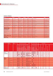
Basic design rules for laser sintering - Handling
Basic design rules for laser sintering - Handling
Basic design rules for laser sintering - Handling

You also want an ePaper? Increase the reach of your titles
YUMPU automatically turns print PDFs into web optimized ePapers that Google loves.
walls / pins<br />
walls<br />
— X/Y<br />
• min possible wall thickness = 0.7 mm <strong>for</strong> P390 /P730<br />
• min possible wall thickness = 0.45 mm <strong>for</strong> P100<br />
• min wall thickness <strong>for</strong> reproducible measurements and mechanical properties = 1.5 mm<br />
— Z<br />
• min possible wall thickness = one Layer; typical 0.15 <strong>for</strong> P390 and 0.10 <strong>for</strong> Formiga<br />
pins<br />
— min pin thickness = 0.8 mm<br />
— min pin thickness <strong>for</strong> reproducible measurement and mechanical properties = 1.8 mm<br />
Source: EOS GmbH<br />
EOS 2012 · <strong>Basic</strong> Design <strong>rules</strong> <strong>for</strong> <strong>laser</strong> <strong>sintering</strong> Page 10