PC-73C Manual - EAGLE Technology
PC-73C Manual - EAGLE Technology
PC-73C Manual - EAGLE Technology

You also want an ePaper? Increase the reach of your titles
YUMPU automatically turns print PDFs into web optimized ePapers that Google loves.
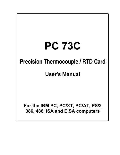
<strong>PC</strong> <strong>73C</strong><br />
Precision Thermocouple / RTD Card<br />
User's <strong>Manual</strong><br />
For the IBM <strong>PC</strong>, <strong>PC</strong>/XT, <strong>PC</strong>/AT, PS/2<br />
386, 486, ISA and EISA computers
All rights reserved. No part of this Publication may be copied, stored in a retrieval<br />
system, or transmitted, in any form by any means, electronic, mechanical, by<br />
photocopying, recording, or otherwise, in whole or in part, without prior written<br />
permission from the Publishers.<br />
Fifth Edition<br />
April 1998<br />
2 April 1998 Printing<br />
Information furnished in this manual is believed to be accurate and reliable; however<br />
no responsibility is assumed for its use, nor for any infringements of patents or other<br />
rights of third parties which may result from its use.<br />
IBM, IBM <strong>PC</strong>/XT/AT and IBM PS/2 are trademarks of International Business<br />
Machine Corporation. MicroSoft and MSDOS are trademarks of MicroSoft<br />
Corporation. All other trademarks used in this manual are the property of their<br />
respective owners.<br />
© Copyright 1996/1998: Shafique Allie (E-mail: shafique@eagle.co.za)<br />
Eagle <strong>Technology</strong> (E-mail: eagle@eagle.co.za)<br />
2
Table of Contents<br />
Introduction 5<br />
Chapter 1: Installation 7<br />
Page<br />
1.1) Setting the Base Address 7<br />
1.2) Wait State Generation on the <strong>PC</strong> <strong>73C</strong> 9<br />
1.3) Interrupt Jumper Settings 10<br />
1.4) Instrumentation Amplifier Gain Settings 11<br />
1.5) Installation 11<br />
Chapter 2: Interconnections 13<br />
2.1) Connections to Backplane of <strong>PC</strong> 13<br />
2.2) Analog Input Connector 13<br />
2.3) Digital Input Connector 14<br />
2.4) Analog Screw Terminal Panel 15<br />
a) Thermocouple Input Module 15<br />
b) RTD Input Module 16<br />
2.5) Power supply connections 16<br />
Chapter 3: Register Structure 17<br />
3.1) ADCHR (A/D Channel, CJC) Register 17<br />
3.2) ADDSR (A/D data/status) Register 18<br />
3.3) ADCNTRL (A/D Control/Status) Register 19<br />
3.4) DIORW (Digital Input/Output) Register 20<br />
Chapter 4: Programming Guide 21<br />
4.1) Initialization 22<br />
4.2) Obtaining a single A/D reading 22<br />
4.3) Overlapping the relay setting time 23<br />
4.4) Converting from binary to analog values 23<br />
a) Thermocouple Inputs 23<br />
b) RTD Inputs 23<br />
c) CJC Input 23<br />
4.5) Writing and reading the digital I/O lines 23<br />
4.6) Interrupt Handling 24<br />
Chapter 5: Driver Software 25<br />
5.1) Board Handles 25<br />
5.2) Interrupt Functions 25<br />
5.3) Quick Reference 26<br />
3
Table of Contents Continued....<br />
Page<br />
Chapter 6: Testing and calibrating the <strong>PC</strong> <strong>73C</strong> 28<br />
6.1) Testing the <strong>PC</strong> <strong>73C</strong> Board 28<br />
6.2) Calibrating <strong>PC</strong> <strong>73C</strong> with thermocouples 28<br />
a) Requirements 29<br />
b) Equipment required 29<br />
c) Procedure 29<br />
6.3) Calibrating <strong>PC</strong> <strong>73C</strong> with RTD inputs 31<br />
a) Requirements 32<br />
b) Equipment Required 32<br />
c) Procedure 33<br />
6.4) Temperature verification 35<br />
Chapter 7: Troubleshooting the <strong>PC</strong> <strong>73C</strong> 36<br />
Chapter 8: Repair Service 39<br />
Chapter 9: Specifications 40<br />
Appendix A: Base Address Settings 42<br />
Appendix B: Layout Diagram 50<br />
4
Introduction<br />
The <strong>PC</strong> <strong>73C</strong> Thermocouple / RTD Input Card is a high accuracy thermoucouple / RTD<br />
measurement subsystem for the IBM <strong>PC</strong>/XT/AT, 486, Pentuim, ISA and EISA Computers. It<br />
provides 8 thermocouple / RTD Inputs via a Screw Terminal Block and 8 digital<br />
inputs/outputs via an auxilliary DB25 Interface Connector. It supports thermocouple types K,<br />
J, E, T, B, R, S, & N as well as 100Ω or 1kΩ RTDs.<br />
The <strong>PC</strong> <strong>73C</strong> fits into one of the IBM 8 bit expansion slot.<br />
Typical applications<br />
¯ Industrial control and temperature measurement<br />
¯ Process Control<br />
¯ Laboratory Automation<br />
¯ Energy management<br />
¯ Product testing<br />
Key Features<br />
¯ On-board wait state generation allows operation on high speed computers<br />
¯ Provides 8 differential input channels for thermocouple or RTD Inputs<br />
¯ Complex noise control circuitry gives accuracies up to ±1 count ( Gain = 100)<br />
¯ 8 Digital Input and 8 Digital Outputs also provided to control other processes<br />
¯ Interrupt support for background sampling<br />
¯ Gains selectable from 1, 10, 100, 200, 500, 600, 700, 800.<br />
¯ EDR Driver software libraries for C, Pascal, Qbasic Basic and Visual Basic is<br />
provided for easy programming.<br />
¯ EDR Driver software libraries (DLL) for Windows V3.11 or Win95 are included<br />
¯ Third Party Software like LabView for Windows, LabTech Notebook, DasyLab and<br />
TestPoint are also provided.<br />
5
<strong>PC</strong> 73 Package<br />
The <strong>PC</strong> <strong>73C</strong> package consists of:<br />
¯ <strong>PC</strong> <strong>73C</strong> Interface Card<br />
¯ <strong>PC</strong> <strong>73C</strong> Auxilliary Card (Thermocouple Module or the RTD Module)<br />
¯ <strong>PC</strong> <strong>73C</strong> User's <strong>Manual</strong><br />
¯ EDR Developers Toolkit User <strong>Manual</strong> + 5¼ or 3½' diskette<br />
¯ A DB25 Male to DB 25 Female Connector Lead<br />
¯ A DB25 type male connector<br />
¯ One 5¼' OR 3½' diskette containing the <strong>PC</strong> <strong>73C</strong> drivers and demonstration software<br />
If any of the items is missing, contact your dealer immediately specifying which components<br />
are missing.<br />
6
Chapter 1: Installation<br />
There are two aspects of the <strong>PC</strong> <strong>73C</strong> that must be configured:<br />
1.1) The Base Address<br />
This address determines where the board is accessed. This can be set by a 8-way<br />
DIP switch found on the <strong>PC</strong> <strong>73C</strong> Board. The address range are from 0 to 7ffh.<br />
1.2) Wait State generation<br />
Some computers have very high I/O bus cycles. In this case it is neccessary to slow<br />
down these cycles when the computer accesses the <strong>PC</strong> <strong>73C</strong> Board. Additional wait<br />
states can be set by means of a jumper on the <strong>PC</strong> <strong>73C</strong> Board.<br />
1.3) Instrumentation amplifier gain setting<br />
Jumpers on board the card determines enables one to select the appropriate gain<br />
settings. Gains can be configured to 1, 10, 100, 200, 500, 600, 700, 800.<br />
1.1) Setting the base address<br />
The <strong>PC</strong> <strong>73C</strong> occupies a block of 4 consecutive I/O addresses. The base address<br />
setting controls where the block starts. This base address must be unique to the <strong>PC</strong><br />
<strong>73C</strong> only and no other card must occupy this address. If multiple <strong>PC</strong> <strong>73C</strong> boards<br />
are installed in one computer then each board must have a different base address.<br />
The base address can be assigned to any location from 0 to 7ffh in 8 byte<br />
boundaries. Table 1 shows the I/O addresses occupied by standard interface cards.<br />
Refer to the Base Address Setting Table in Appendix A for a list of the various<br />
base address settings that the <strong>PC</strong> <strong>73C</strong> can occupy.<br />
The base address setting can be set by adjusting the 8-way dip switch on the <strong>PC</strong><br />
<strong>73C</strong>. Each line on the DIP switch switch compares an address line in I/O space.<br />
Switch number 1 compares address line A10; switch number 2: address A9 while<br />
switch number 8 compares address line A3. Factory default setting is 300h.<br />
If one of the switches are OFF, then it contributes to the base address. An example<br />
is as follows:<br />
Base Address = Switch 2 (Address A9) + Switch 3 (address A8)<br />
= 200 + 100<br />
= 300h<br />
7
Table 1: Addresses for standard I/O devices<br />
Address Standard device<br />
000-1FF Internal system board<br />
200-20F Games port<br />
210-217 Expansion unit<br />
220-24F Reserved<br />
250-257 Not assigned<br />
258-25F Intel 'Above Board'<br />
260-277 Not assigned<br />
278-26F Reserved<br />
280-2EF Not assigned<br />
2F0-2F7 LPT2<br />
2F8-2FF COM2<br />
300-31F Prototype Board<br />
320-32F Hard Disk<br />
330-377 Not assigned<br />
378-37F LPT1<br />
380-38F SDLC communications<br />
390-39F Not assigned<br />
3A0-3AF Binary comms<br />
3B0-3BF Mono Display Adaptor<br />
3C0-3CF Reserved<br />
3D0-3DF CGA<br />
3E0-3E7 Reserved<br />
3E3-3EF Not assigned<br />
3F0-3F7 Floppy disk<br />
3F8-3FF COM1<br />
400-FFF Not used see below<br />
Table 1: Standard I/O Addresses<br />
ON<br />
1 2 3<br />
4 5 6 7 8<br />
400 200 100 80 40 20 10 8 Hex Weight when OFF<br />
A10 A9 A8 A7 A6 A5 A4 A3 Corresponding Address line<br />
Figure 1:<br />
Dip Switch Address Weight (in Hex)<br />
8
Note that addresses from 400h-7FFh cannot normally be used because these addresses are not<br />
normally decoded by some cards and I/O devices in the 0h to 3FFh range.<br />
The <strong>PC</strong> <strong>73C</strong> Thermocouple / RTD board however (and most other members of the <strong>PC</strong>-XX<br />
family) can use these address, if and only if the board at address 400h less than the address of<br />
the <strong>PC</strong> <strong>73C</strong> also decodes the extra address.<br />
For example, a <strong>PC</strong> <strong>73C</strong> can be installed at address 300h and another one at address 700h<br />
(400h locations apart). However, it would not be advisable to install a <strong>PC</strong> <strong>73C</strong> at address<br />
7F8h. This is because communications port COM1 is installed at 3F8h and does not normally<br />
decode these extra addresses.<br />
If your computer has boards not listed in Table 1 (such as LAN adaptors, back-up boards or<br />
other engineering boards), you should consult the User's <strong>Manual</strong>s for these boards for<br />
information on the address ranges used.<br />
In most cases, base address of 300h is a good choice. Address 300h is also the factory default<br />
base address setting.<br />
1.2) Wait State Generation on the <strong>PC</strong> <strong>73C</strong><br />
Additional wait states can be inserted in the I/O bus cycle by changing the jumper setting<br />
on JP1 on the <strong>PC</strong> <strong>73C</strong>. This jumper is marked 'Wait State Jumper' on the <strong>PC</strong> <strong>73C</strong> board.<br />
Refer to figure 1.2 for the wait state jumper settings. Note that the factory default setting<br />
is zero wait states.<br />
Figure 1.2: Wait State Jumper config<br />
In most cases, only a very small number of computers require additional wait states. If<br />
the <strong>PC</strong> <strong>73C</strong> seems to be giving incorrect results then try increasing the wait states until<br />
correct results are obtained. If the board still does not produce correct results even after<br />
the maximum number of wait states has been inserted then the <strong>PC</strong> <strong>73C</strong> or the host<br />
computer are defective and should be serviced.<br />
9
1.3) Interrupt Jumper Settings<br />
If the external trigger option is used, then it is necessary to configure the interrupt jumper<br />
settings. Refer to figure 3 for the interrupt jumper settings.<br />
Figure 3: Interrupt jumper settings<br />
In a standard <strong>PC</strong>, the interrupt levels are allocated as follows:<br />
Level Level<br />
IRQ0<br />
IRQ1<br />
IRQ2/IRQ9<br />
IRQ3<br />
IRQ4<br />
IRQ5<br />
IRQ6<br />
IRQ7<br />
Allocation<br />
System timer<br />
Keyboard<br />
Display Adaptor<br />
COM1 (if installed)<br />
COM2 (if installed)<br />
LPT2 (if installed)<br />
Floppy disk controller<br />
LPT1 (if installed)<br />
Table 2: Standard interrupt settings<br />
On <strong>PC</strong> ATs, IRQ2 is used by the system board itself and any interrupt requests on IRQ2 is<br />
transparently rerouted to IRQ9.<br />
The default IRQ setting on the <strong>PC</strong> <strong>73C</strong> is IRQ7. Note that unless the interrupt line is<br />
specifically enabled by software, the interrupt output from the <strong>PC</strong> <strong>73C</strong> is tri-stated (ie: not<br />
connected). It is also tri-stated upon power-up.<br />
10
1.4) Instrumentation Amplifier Gain Settings<br />
Gain settings can be set via Jumpers JP4. Check the silkscreen text on the <strong>PC</strong> <strong>73C</strong> to<br />
select the appropriate gain setting.<br />
JP5 JP5 JP5 JP5 JP5<br />
200<br />
500<br />
100<br />
10<br />
200<br />
500<br />
100<br />
10<br />
200<br />
500<br />
100<br />
10<br />
200<br />
500<br />
100<br />
10<br />
200<br />
500<br />
100<br />
10<br />
gain 1<br />
gain 10<br />
gain 100<br />
gain 200<br />
gain 300<br />
JP5 JP5 JP5 JP5<br />
200<br />
500<br />
100<br />
10<br />
200<br />
500<br />
100<br />
10<br />
200<br />
500<br />
100<br />
10<br />
200<br />
500<br />
100<br />
10<br />
gain 500<br />
gain 600<br />
gain 700<br />
gain 800<br />
Figure 1.3: Gain Jumper Settings<br />
1.5) Installation<br />
Requirements:<br />
¯ XT/286/386/486, ISA, EISA, Pentium Computer<br />
¯ Phillips Screw Driver (or one to match screw on the computer cabinet and<br />
bracket)<br />
¯ 8 bit or 16 bit bus slot<br />
Procedure:<br />
a) Switch off the computer and all attached devices<br />
b) Unplug power cord from the computer and all attached devices.<br />
+ Warning<br />
Failure to disconnect all power cables can result in harzardous conditions, as<br />
there may be dangerous voltage levels present in externally connected cables.<br />
c) Remove the top cover from the <strong>PC</strong>. If you are not sure how to do this, consult the<br />
manual supplied with the system unit.<br />
11
d) Choose any 8 or 16 bit expansion slot and remove the screw from the metal bracket<br />
fixed corresponding to the chosen slot.<br />
e) Align the gold plated edge connector with the edge socket and the rear adaptor slot with<br />
the board bracket. Firmly press the board down into the socket on the computer's system<br />
board. Ensure that the board's edge connector is in the socket and has not slipped<br />
sideways past the socket.<br />
f) Replace the screw on the bracket and tighten the screw to the back panel.<br />
g) Replace the computer's cover. Plug in all cables and switch the computer power on. The<br />
<strong>PC</strong> <strong>73C</strong> is now installed.<br />
12
CHAPTER 2: Interconnections<br />
The <strong>PC</strong> <strong>73C</strong> thermocouple board plugs into any ISA expansion slot at the gold finger edge<br />
connectors J1/J2. The board communicates to the user circuit via connectors mounted on the<br />
bracket. This chapter describes these connectors<br />
2.1) Connections to the IBM Bus<br />
The <strong>PC</strong> <strong>73C</strong> board may be plugged into any slot of the computer backplane with the<br />
exception of J8 slot of the IBM XTs. All data transfers to and from the host computer is<br />
channelled via this connector.<br />
2.2) Analog Input Connector<br />
The <strong>PC</strong> <strong>73C</strong> interfaces to the external world via two 25-way D-type male connectors. The<br />
first connector (refer to Figure 4) accommodates the following signals and is connected<br />
via a cable to the <strong>PC</strong> <strong>73C</strong> screw terminal board:<br />
¯ 8 differential input channels<br />
¯ +5V, +12V power supply and analog ground<br />
Figure 4: <strong>PC</strong> <strong>73C</strong> Interface Connector<br />
(as seen from the rear of the <strong>PC</strong>)<br />
Figure 4 graphically shows the connector together with their pin assignments. Note that<br />
the pin connections refer to the pin numbers of the connector when looking into the<br />
connector from the rear of the computer. Also note that the pin numbers are embossed on<br />
the connector itself.<br />
13
2.3) Digital Input Connector<br />
The second connector is used for the Digital I/O signals and have the following signals:<br />
i) 8 digital input channels<br />
ii) 8 digital output channels<br />
iii) +5V power supply and digital ground<br />
The second connector maps an IDC header connector to a DB25 male connector (figure 5).<br />
This cable is supplied with the <strong>PC</strong><strong>73C</strong> Board.<br />
Digital Output 7<br />
Digital Output 6<br />
Digital Output 5<br />
Digital Output 4<br />
Digital Output 3<br />
Digital Output 2<br />
Digital Output 1<br />
Digital Output 0<br />
Digital Ground<br />
Digital Input 6<br />
Digital Input 4<br />
Digital Input 2<br />
Digital Input 0<br />
13<br />
12<br />
11<br />
10<br />
9<br />
8<br />
7<br />
6<br />
5<br />
4<br />
3<br />
2<br />
1<br />
25<br />
24<br />
23<br />
22<br />
21<br />
20<br />
19<br />
18<br />
17<br />
16<br />
15<br />
14<br />
+5V<br />
Digital Ground<br />
Digital Ground<br />
Digital Ground<br />
Digital Ground<br />
Digital Ground<br />
Digital Ground<br />
Digital Ground<br />
Digital Input 7<br />
Digital Input 5<br />
Digital Input 3<br />
Digital Input 1<br />
Figure 5: Digital I/O connector<br />
Figure 5 graphically shows the digital I/O connector together with their pin assignments.<br />
Note that the pin connections refer to the pin numbers of the connector when looking into<br />
the connector from the rear of the computer. Also note that the pin numbers are embossed<br />
on the connector itself.<br />
14
2.4) The Analog Screw Terminal Panel<br />
This panel connects to the analog input connector via a DB25 cable. The <strong>PC</strong> <strong>73C</strong> is<br />
intended for connection of exposed or ungrounded type thermocouples while the RTD<br />
Module can handle 100R [PT100] or 1kΩ [PT1000] Resistors. All that is required is to<br />
connect the two thermocouple leads to the <strong>PC</strong> <strong>73C</strong> terminal block.<br />
a) Thermocouple Module<br />
Figure 7a below shows the terminal block for thermocouples.<br />
CHAN 0<br />
CHAN 1<br />
CHAN 2<br />
CHAN 3<br />
CHAN 4<br />
CHAN 5<br />
CHAN 6<br />
CHAN 7<br />
Figure 7a: <strong>PC</strong> <strong>73C</strong> Terminal Block<br />
+ Warning<br />
Note that both leads on any thermocouple connected to the <strong>PC</strong> <strong>73C</strong> must be<br />
completely isolated. The <strong>PC</strong> <strong>73C</strong> itself does not have isolated inputs. Do not<br />
ground either the thermocouples lead, or use grounded junction thermocouples<br />
15
) RTD Input Module<br />
Figure 7b below shows the terminal block for the RTD Input Board<br />
2.5) Power supply connections<br />
Figure 7a: RTD Module Layout Diagram<br />
The +5V power with digital ground are available on the digital DB25 output connector in<br />
order to drive external circuitry. However, maximum permissible current drive is 500mA.<br />
16
CHAPTER 3: Register Structure<br />
At the lowest level, the <strong>PC</strong> <strong>73C</strong> can be programmed using I/O input and output instructions.<br />
This chapter contains the information on all the <strong>PC</strong> <strong>73C</strong> registers. Although programming the<br />
board is not difficult, it is time consuming and requires detailed knowledge of the <strong>PC</strong> <strong>73C</strong> as<br />
well as the operation of the host <strong>PC</strong> and its operating system. In order to simplify the process,<br />
a set of driver libraries is provided. The use of these libraries allow access to all the board's<br />
functions and is described in Chapter 5: Programming guide.<br />
The <strong>PC</strong> <strong>73C</strong> occupies 4 consecutive addresses in the computer's I/O space. The layout of<br />
these registers are shown in Table 4: <strong>PC</strong> <strong>73C</strong> register structure. The offset of the registers are<br />
given as offset addresses from the base address of the board. This base address is set with the<br />
Dip Switch as detailed in Chapter 2: Installation.<br />
Offset Read Write<br />
0 Channel Register (ADCHR) Channel Register (ADCHR)<br />
1 A/D Data / Status (ADDSR)<br />
2 A/D Control (ADCNTRL) A/D Control (ADCNTRL)<br />
3 Digital Input (DIORW) Digital Output (DIORW)<br />
Table 4: <strong>PC</strong> <strong>73C</strong> register structure<br />
3.1) ADCHR - Channel Register (offset 0, read/write)<br />
This register controls the 8 analog input channels and the Cold Junction Compensation<br />
(CJC) channel.<br />
ADCHR Register (read mode)<br />
Bit 7 Bit 6 Bit 5 Bit 4 Bit 3 Bit 2 Bit 1 Bit 0<br />
x x x CJC x CH2 CH1 CH0<br />
ADCHR Register (write mode)<br />
Bit 7 Bit 6 Bit 5 Bit 4 Bit 3 Bit 2 Bit 1 Bit 0<br />
0 0 0 CJC 0 CH2 CH1 CH0<br />
Bit 0 thru 2: The bits specify a three channel address. A write to these bits determines the<br />
channel that will be converted on the next A/D strobe if and only if the CJC bit is<br />
clear.<br />
Reading these bits determines the channel that is currently converted on the A/D<br />
strobe.<br />
Bit 3<br />
Reserved for manufacturing tests. Write 0 to these bits in order to maintain future<br />
compatibility. Reading these bits are undefined.<br />
17
Bit 4:<br />
This bit controls the cold junction compensation temperature. If this bit is set<br />
then the CJC temperature is read on the next A/D strobe. If a zero is written then<br />
the the thermocouple input channel indicated by the channel bits is read.<br />
Reading this bit reflect the status of the CJC bit.<br />
Bits 5 to 7: Reserved for manufacturing tests. Write a 0 to these bits. Reading these bits are<br />
undefined.<br />
3.2) ADDSR - A/D data/status Register (offset 1, read only)<br />
This register contains either:<br />
¯ The least significant byte of the A/D result, or<br />
¯ The Upper 4 Bits of the A/D result and the A/D Status<br />
The Register function is selected by HBEN and LBEN bits in the Control Register<br />
ADDSR Register (read mode)<br />
Bit 7 Bit 6 Bit 5 Bit 4 Bit 3 Bit 2 Bit 1 Bit 0<br />
AD7 AD6 AD5 AD4 AD3 AD2 AD1 AD0<br />
HBEN LBEN<br />
1 0<br />
ADDSR Register (read mode)<br />
Bit 7 Bit 6 Bit 5 Bit 4 Bit 3 Bit 2 Bit 1 Bit 0<br />
POL OVR x x AD11 AD10 AD9 AD8<br />
HBEN LBEN<br />
0 1<br />
Bit 0 to 7:<br />
If bits HBEN is set and LBEN reset in the Control Register (CNTRL) then the<br />
data read is the Least Significant Byte (AD0 to AD7) of the 12 bit data value<br />
+ Note<br />
If bits HBEN is reset and LBEN set in the Control Register (CNTRL) then the<br />
data bits read are as follows:<br />
Bit 0 to 3: If read, it gives the upper 4 bits of the A/D result.<br />
Bit 4, 5:<br />
Bit 6:<br />
Bit 7:<br />
These bits are undefined when read<br />
This is the overrange bit. If it is set then the measured voltage is out of the<br />
A/D convertor's range.<br />
This is the polarity bit. If it is set then the measured voltage is positive.<br />
18
3.3) ADCNTRL - A/D Control/Status register (offset 2: read/write)<br />
This register contains control/status bits for the A/D, Interrupt Enable and the Multiplexor<br />
Enable.<br />
ADCNTRL Register (write mode)<br />
Bit 7 Bit 6 Bit 5 Bit 4 Bit 3 Bit 2 Bit 1 Bit 0<br />
MUXEN RUN HBEN LBEN 0 IRQEN 0 0<br />
ADCNTRL Register (read mode)<br />
Bit 7 Bit 6 Bit 5 Bit 4 Bit 3 Bit 2 Bit 1 Bit 0<br />
MUXEN RUN HBEN LBEN x IRQEN x STS<br />
Bit 0:<br />
Bit 1:<br />
Bit 2:<br />
Bit 3:<br />
Bit 4:<br />
Bit 5:<br />
Determines the status of the A/D convertor. Once the A/D conversion begins, the<br />
STS bit goes high. When the A/D conversion is ready, the STS bit returns low.<br />
Reserved for manufacturing tests. Write a 0 to this bit. Reading these bit is<br />
undefined.<br />
Controls the interrupt line. Setting this bit to 1 enables the interrupt line while<br />
setting the bit to 0 disables the line. Note that bit 0 is set to 0 upon power up.<br />
Reading back this bit provides the status of the interrupt enable line.<br />
Reserved for manufacturing tests. Write a 0 to this bit. Reading these bit is<br />
undefined.<br />
This bit (LBEN) controls the data from the A/D convertor. When LBEN is set<br />
low then the lower 8 bits of the A/D result appear in the ADDSR register.<br />
Reading this bit determines the status of the LBEN line.<br />
This bit (HBEN) also control the data flow from the A/D convertor. If the HBEN<br />
bit is set low, then the high 4 bits of the A/D result and the A/D status bits appear<br />
in the ADSSR register. Reading this bit determines the status of the HBEN line.<br />
Note: HBEN and LBEN must never be 0 simultaneously. It is advisable to set<br />
both bits high prior t osetting either low.<br />
Bit 6: In order to start a conversion this bit must be set to 1. Bits 4 (LBEN) and 5<br />
(HBEN) must be set to 1 and all other bits to 0. Once the STS bit has gone high<br />
and then returned to 0, the RUN bit may be cleared.<br />
19
Bit 7:<br />
This bit control the Enable line of the Multiplexer. Before attempting to select a<br />
channel (ie: bits CH0 - CH2 in the ADCHR register), one must write a 1 to this<br />
bit. Writing a 0 to this line disables channel selection. Note that this bit is set to 0<br />
upon power up. Reading back this bit provides the status of the Multiplexer<br />
Enable Line.<br />
3.4) DIORW - Digital I/O Read/Write Register (Offset 3, read/write)<br />
This register is used to control the digital I/O lines also available on the <strong>PC</strong> <strong>73C</strong>.<br />
+ Compatibility with <strong>PC</strong>73<br />
On the old <strong>PC</strong> 73 / <strong>PC</strong> 73A Card this register was the MODE register. On these Cards<br />
you were required to write 10000010b (83hex). On the <strong>PC</strong> <strong>73C</strong> Card, this is not<br />
required.<br />
On the <strong>PC</strong><strong>73C</strong> this register is a digital input / output port.<br />
DIOW Register (Write Mode)<br />
Bit 7 Bit 6 Bit 5 Bit 4 Bit 3 Bit 2 Bit 1 Bit 0<br />
D7 D6 D5 D4 D3 D2 D1 D0<br />
Bits 0-7:<br />
Writing any byte from 0 to FFh will set the DIO lines.<br />
+ Caution<br />
Note that you cannot read these lines. A separate DIOR latch is available for<br />
feeding in 8 Input lines. If you want to read these lines, you must connect the<br />
appropriate digital output lines to the digital input lines on the DB25 female<br />
connector.<br />
DIOR Register (Read Mode)<br />
Bit 7 Bit 6 Bit 5 Bit 4 Bit 3 Bit 2 Bit 1 Bit 0<br />
D7 D6 D5 D4 D3 D2 D1 D0<br />
Bits 0-7:<br />
Reading these bits determines the status on the Digital Input Latch available on<br />
the Auxiliary Digital Input connector.<br />
20
Chapter 4: Programming Guide<br />
This chapter describes programming the <strong>PC</strong> <strong>73C</strong> at its lowest level. In order to accomplish<br />
this, detailed knowledge of chapter 4 and the system hardware is required.<br />
As an alternative to low level programming, driver software is provided with the <strong>PC</strong> <strong>73C</strong>. This<br />
is described in Chapter 5.<br />
The advantages of using the driver software are:<br />
a) Detailed knowledge of the <strong>PC</strong> <strong>73C</strong> is not required.<br />
b) The Driver Libraries supports multiple boards. In other words, you can cascade boards in<br />
the same computer.<br />
c) The Driver Library is callable from most high level languages.<br />
Programmers who need to incorporate special routines into their application will need to<br />
read this chapter. Examples are application programs written in Clarion, Clipper, etc.<br />
Once the <strong>PC</strong> <strong>73C</strong> has been installed into the computer and external connections are made,<br />
the board is in an operational state. The <strong>PC</strong> <strong>73C</strong> occupies 4 consecutive I/O addresses<br />
starting from the board's base address. The base address is set by the DIP Switch on the <strong>PC</strong><br />
<strong>73C</strong>. Programming the <strong>PC</strong> <strong>73C</strong> is done by using the input/output instructions. Reading and<br />
writing to these addresses allows data to be moved to and from the <strong>PC</strong> <strong>73C</strong>.<br />
Reading and writing to these ports typically takes on the form of one of the following<br />
instructions:<br />
Language Port Read Port Write<br />
'C' value = inp(addre); outp( addre, value);<br />
Pascal value := port[addre]; port[addre] := value;<br />
Assembly mov al, value mov al, value<br />
mov dx, addre mov dx, addre<br />
in al, dx<br />
out dx, al<br />
where:<br />
addre is the I/O location of the <strong>PC</strong> <strong>73C</strong> registers<br />
value is the byte read or written to the register<br />
21
4.1) Initialization<br />
It is preferred to initialize the <strong>PC</strong> <strong>73C</strong> to a known state before performing certain tasks.<br />
Note that it is not necessary to perform the procedure because all registers are set to a<br />
known state upon power-up.<br />
Procedure:<br />
a) Write 90h to the ADCNTRL Register (offset +2).<br />
b) Write 0h to the ADCHR (offset + 0).<br />
4.2) Obtaining a single A/D reading<br />
To obtain a single reading under program control, proceed as follows:<br />
a) Write the address of the channel you wish to convert, to the ADCHR register (offset +<br />
0)<br />
b) Wait for at least 1ms to allow the relay multplexers to settle.<br />
c) Write F0 (hex) to the ADCNTRL register.<br />
d) Wait for the STS bit in the ADCNTRL register to go high, then low.<br />
e) Write B0 (hex) to the ADCNTRL register.<br />
f) Write A0 (hex) to the ADCNTRL register<br />
g) Read in the low byte of the A/D result from the ADDSR register<br />
h) Write 90 (hex) to the ADCNTRL register<br />
i) Read in the four high bits of the A/D result, the polarity, overrange bits from the<br />
ADDSR register.<br />
j) Write B0 (hex) to the ADCNTRL register.<br />
k) If the polarity bit was high, then the result is positive, else negative.<br />
4.3) Overlapping Relay setting time<br />
If a number of A/D samples is to be obtained, then the relay setting time and the A/D<br />
convertor auto-zero period can be overlapped, improving the <strong>PC</strong> <strong>73C</strong>'s throughput. In<br />
order to do this, the next channel address must be written to the channel register as soon<br />
as the STS returns low on the current sample. If this is done then the 1 ms time delay can<br />
be omitted.<br />
22
4.4) Converting from binary to analog values<br />
Analog data from the A/D convertor is always in a form of a binary code with a sign bit.<br />
Analog voltages may be calculated from the digital codes by simply noting that one LSB<br />
has a specific weight for each instrumentation amplifier gain. It is thus only necessary to<br />
only multiply the integer result from the A/D by this weight.<br />
a) Thermocouple Inputs<br />
For thermocouple inputs, the bit weights are as follows:<br />
b) RTD Inputs<br />
GAIN<br />
BIT WEIGHT<br />
100 (default) 10µV<br />
1 1mV<br />
200 5µV<br />
500 2µV<br />
For RTD inputs, the bit weights are as follows:<br />
GAIN<br />
BIT WEIGHT<br />
100 10µV<br />
1 (default) 1mV<br />
200 5µV<br />
500 2µV<br />
The recommended gain for the RTD module is 1.<br />
c) Cold junction compensation input<br />
For the cold junction compensation input, the bit weight is as follows<br />
Bit Weight<br />
1mV<br />
This results in an effective bit weight of 0.1°C per bit.<br />
4.5) Writing and reading the Digital I/O lines<br />
It is fairly simple to access the Digital Input / Output lines on the <strong>PC</strong> <strong>73C</strong>. Writing to the<br />
digital I/O is done simply by writing the appropriate hex value to the DIOWR register<br />
(Base+3). Reading the digital input lines is done by reading the DIOWR register (Base<br />
+3).<br />
Note that any unconnected digital input lines should be shorted to ground.<br />
23
4.6) Interrupt Handling<br />
The STS line of the A/D is connected to the interrupt line on the <strong>PC</strong>'s I/O channel. This<br />
allows every A/D sample to be read in the background (via an IRQ).<br />
Operation of the ISR is as follows:<br />
a) Save old interrupt vector corresponding to the desired interrupt.<br />
b) Set the interrupt vector in the computer's interrupt vector table corresponding to the<br />
desired IRQ to point to the interrupt service routine that will service the interrupt.<br />
c) Write a 4 to the ADCNTRL register (offset + 2) in order to enable the external interrupt<br />
buffer on the <strong>PC</strong> <strong>73C</strong>.<br />
d) The signal from the A/D convertor is initially low. When an A/D sample is available, the<br />
STS bit goes high, it is bufferred by the <strong>PC</strong> <strong>73C</strong> and activates the corresponding IRQ<br />
line on the <strong>PC</strong> Bus.<br />
e) This causes the host computer to execute the interrupt service routine to allow the A/D<br />
sample to be read from the A/D convertor.<br />
The ISR must contain the following statement to allow further interrupts to be received:<br />
i) It must contain an end of interrupt (EOI) command to the interrupt controller on the<br />
computer system board.<br />
24
Chapter 5: Driver Software<br />
Full driver software is supplied with the <strong>PC</strong> <strong>73C</strong> package. Full details are explained in the<br />
EDR Software developers kit User <strong>Manual</strong>. A summary of the driver functions is explained<br />
below.<br />
Both DOS and Windows Languages are supported: They are:<br />
DOS Languages:<br />
Borland C/C++ Version 3.1 or 4.0<br />
Microsoft C/C++ Version 6.0 or 7.0<br />
Borland Pascal / Turbo Pascal Version 6.0 or 7.0<br />
Microsoft QuickBasic Version 4.5<br />
Windows Languages:<br />
Delphi V1.00 / V2.00 / V3.00 / V4.00<br />
Borland C/C++ 3.1 / 4.0 / 5.0<br />
Microsoft C/C++ 6.0 or 7.0<br />
Borland Pascal / Turbo Pascal Version 6.0 or 7.0<br />
Visual Basic V1.00 thru V5.00<br />
Other compilers can also be supported if they can call functions from a DLL.<br />
5.1) Board Handles<br />
All EDR functions used above require a board handle as the first parameter. The board<br />
handle defines which board is affected by the function call. Using this method has several<br />
advantages, For example, there is no need for a 'select board' function; working with<br />
parallel boards is much easier; different applications using the EDR at the same time will<br />
not conflict with each other.<br />
Board handles are integers obtained by calling EDR_AllocBoardHandle (see 7.2 of EDR<br />
Developers Toolkit). Once allocated a board handle must be initialised to the <strong>PC</strong> <strong>73C</strong><br />
before it can be accessed. This is achieved by calling EDR_InitBoard or<br />
EDR_InitBoardType (see 7.5 of EDR manual) with the base address or<br />
EDR_loadConfiguration (see section 7.8 of EDR manual).<br />
EDR_InitBoard will attempt to detect the <strong>PC</strong><strong>73C</strong> at the base address specified.<br />
5.2) Interrupt functions<br />
Since the STS line of the A/D convertor on the <strong>PC</strong> <strong>73C</strong> is connected to the hardware<br />
interrupt, an ISR can be installed using the EDR driver functions to obtain A/D samples<br />
in background mode.<br />
These functions are only callable from virtually any programming language. See the EDR<br />
Software Developers Kit Reference <strong>Manual</strong>.<br />
25
5.3) Quick Function Reference<br />
The <strong>PC</strong> <strong>73C</strong> Enhanced Thermocouple Board utilises the following functions calls<br />
contained in the EDR driver developers toolkit. They are:<br />
Function Name<br />
EDR_ADInOneVoltage<br />
EDR_GetCJCChannelNum<br />
EDR_CalcCJCmC<br />
EDR_CalcTCmC<br />
EDR_CalcRTDmC<br />
EDR_SetADClockmilliHz<br />
EDR_SetADTransferMode<br />
EDR_ADInBinBackground<br />
EDR_ADInBinCircularBuffer<br />
EDR_InstallISR<br />
EDR_UninstallISR<br />
EDR_InstallBoardISR<br />
EDR_UninstallBoardISR<br />
EDR_MaskIRQ<br />
EDR_MaskBoardIRQ<br />
Description<br />
Obtains a single A/D reading in normal mode<br />
Returns the channel number of the <strong>PC</strong> <strong>73C</strong>'s CJC<br />
input.<br />
Converts a microvolt value read from the CJC<br />
channel into a value in milli °C.<br />
Converts a microvolt value read from a TC channel<br />
into a temperature in milli °C compensating for the<br />
ambient temperature at the junction block. It<br />
requires that you specify what type of<br />
thermocouple is being used and the ambient<br />
temperature. EDR supports 8 different TC types<br />
listed in Appendix A.21 in the EDR Driver<br />
<strong>Manual</strong>.<br />
Converts a microvolt value read from the RTD<br />
channel into a temperature in milli °C. This<br />
function assumes that you are using our RTD board<br />
(ie: <strong>PC</strong> <strong>73C</strong>-R).<br />
Sets the clock frequency using the <strong>PC</strong>'s timer tick<br />
interrupt<br />
Set the transfer mode used to obtain data from the<br />
<strong>PC</strong> <strong>73C</strong> (use EDR_INTR for interrupt sampling)<br />
Acquires a block of A/D data from the channels in<br />
the channels list in the background<br />
Similar to EDR_ADInBinBackground but treats<br />
sample buffer as a ring buffer<br />
Installs an ISR for the specified hardware interrupt<br />
request<br />
Removes an interrupt service routine that was<br />
installed with EDR_InstallISR<br />
Installs an ISR for a particular type of interrupt<br />
installed on the <strong>PC</strong> <strong>73C</strong>.<br />
Removes an interrupt service routine that was<br />
installed with EDR_InstallBoardISR<br />
Masks or unmasks a particular IRQ level<br />
Masks or unmasks a particular board interrupt<br />
26
Function Name<br />
EDR_EnableInterrupt<br />
EDR_ResetInterrupt<br />
EDR_AllocBoardHandle<br />
EDR_FreeBoardHandle<br />
EDR_InitBoardType<br />
EDR_ConfigDialog<br />
EDR_SaveConfiguration<br />
EDR_LoadConfiguration<br />
EDR_RestoreDefaults<br />
EDR_IsBaseAddressInUse<br />
EDR_DetectBoard<br />
EDR_SetBoardType<br />
EDR_SetIRQLevel<br />
EDR_SetIRQLevel<br />
EDR_DIOLineInput<br />
EDR_DIOLineOutput<br />
EDR_DIOPortInput<br />
EDR_DIOPortOutput<br />
Description<br />
Enables / disables a specified interrupt on hte <strong>PC</strong><br />
<strong>73C</strong><br />
Sends an EOI command to one of the <strong>PC</strong>s interrupt<br />
controllers on completion of the interrupt<br />
Allocates a new board handle to the <strong>PC</strong> <strong>73C</strong>. If no<br />
board handles are available then a 0 is returned.<br />
This is particularly useful is multiple <strong>PC</strong> <strong>73C</strong> are<br />
present in the same.computer.<br />
Releases a board handle allocated to the <strong>PC</strong> <strong>73C</strong><br />
making it available to any other <strong>PC</strong> card<br />
Initialises a board and allocates a board handle to it<br />
Diplays a dialog box that allows the user to<br />
manually configure the driver for the Board in the<br />
computer<br />
Function writes configuration information to a file<br />
for later loading with EDR_LoadConfiguration<br />
Loads details of the Cards configuration from the<br />
file created by EDR_SaveConfiguration<br />
Restores factory default configuration for a baord<br />
attached to a handle<br />
Checks if any board initialised with EDR is using<br />
the specified I/O address<br />
Tries to determine the type of board present at a<br />
specified I/O address.<br />
Changes the board type attached to a board handle<br />
Set the IRQ level EDR will use for the interrupt ID<br />
specified.<br />
Set the IRQ level EDR will use for the interrupt ID<br />
specified.<br />
Gets the status of a single line in a digital input<br />
port.<br />
Changes a single line (bit) in a digital output port<br />
Reads a byte of data from a digital input port<br />
Writes a byte of data to a digital output port<br />
27
Chapter 6: Testing and Calibrating the <strong>PC</strong> <strong>73C</strong><br />
Before attempting to interface the <strong>PC</strong> <strong>73C</strong> with your application, it is essential that you<br />
test the board first. This is done using the following procedure:<br />
6.1) Testing the <strong>PC</strong> <strong>73C</strong> Board<br />
Install the <strong>PC</strong> <strong>73C</strong> using the procedure described in the Chapter 2: Installation. Proceed as<br />
follows:<br />
¯ Switch the Computer on<br />
¯ On the DOS prompt, go to the C:\EDR\TPAS\DEMOS\ sub-directory<br />
¯ If you have the thermocouple interface then run the TEMPMETR.EXE test program<br />
with parameter 300 where 300 is the base address of the <strong>PC</strong> <strong>73C</strong>.<br />
¯ If you have the RTD interface module then run the RTDMETR.EXE test program in<br />
the C:\EDR\TPAS\DEMOS\ sub-directory with parameter 300 where 300 is the base<br />
address of the <strong>PC</strong> <strong>73C</strong>.<br />
If an error message 'Board not found' appears on your screen then the <strong>PC</strong> <strong>73C</strong> was not<br />
installed at that address. Try a different base address as specified in Apendix A (eg: 700h)<br />
and re-run the test S/W. If the problem persists then try increasing the wait states on the<br />
<strong>PC</strong> <strong>73C</strong> Board and re-run test software. The board should work.<br />
If the <strong>PC</strong> <strong>73C</strong> is found, a message will appear on the screen: '<strong>PC</strong> <strong>73C</strong> Board found'. The<br />
program will display the channels 1 thru 8 and the ambient temperature.<br />
6.2) Calibrating the <strong>PC</strong> <strong>73C</strong> Board with the thermocouple module<br />
This procedure should be performed at six month intervals or whenever the<br />
input range jumpers are changed.<br />
+ Before attempting to calibrate the <strong>PC</strong> <strong>73C</strong> Board, allow the host <strong>PC</strong> and the<br />
<strong>PC</strong> <strong>73C</strong> to warm up for at least one hour before calibration<br />
A/D calibration is performed by adjusting the gain [VR1] and offset trimpots [VR3<br />
(channel 1) thru VR10 (channel 8)] on the <strong>PC</strong> <strong>73C</strong> <strong>PC</strong>B. These trimpots are easily located<br />
from the board layout as shown in Appendix B. Note that you can use the silkscreen text<br />
on the <strong>PC</strong> <strong>73C</strong> as a reference.<br />
28
a) Requirements<br />
i) Calibration is done on all the channels. The recommended connector wiring is to<br />
connect all the channels +ve inputs together and all the -ve inputs together.<br />
ii) Calibration is performed with the board jumpered into its intended operating mode.<br />
iii) All cables should be as short as possible.<br />
b) Equipment required<br />
i) Precision voltage source with ±10V output range with absolute accuracy better than<br />
0.005%, resolution 100nV or better.<br />
c) Procedure<br />
i) Run the TEMPMETR.EXE program found in the C:\EDR\C\DEMOS directory.<br />
ii) Apply 0.01mV to all the channels. Adjust the offset trimpot for an output code which<br />
flickers between 0 and 1.<br />
iii) Apply 40.95mV (+FS -¾LSB) for a gain of 100 to channel 0 (you do not need to look<br />
at the other channels). If you choose any other gains then check the table below to<br />
select appropriate full scale -¾LSB voltage.<br />
Gain<br />
+FS -¾LSB<br />
1 4.095V<br />
10 409.5mV<br />
100 40.95mV<br />
200 20.4725mV<br />
300 13.65mV<br />
500 8.1890mV<br />
600 6.827mV<br />
700 5.851mV<br />
Adjust the gain trimpot (VR1) for an output code which flickers evenly between 4094<br />
and 4095.<br />
29
iv) Repeat the above two steps until no further adjustment is required.<br />
+ NOTE<br />
You may find some difficulty in setting the channel offset calibration to zero<br />
when turning the Offset Voltage trimpots because of excessive enviromental<br />
noise on the ground lines. You can adjust the offset voltage to between ±2<br />
counts. Then calibrate the full scale voltage using the Gain Trimpot (VR1).<br />
Repeat the offset voltage adjustment again and try to adjust the channels to ±1<br />
count. Calibrate the full scale voltage again using the Gain Trimpot (VR1)<br />
[this might not be needed].<br />
30
6.3) Calibrating the <strong>PC</strong> <strong>73C</strong> Board with the RTD module<br />
This procedure should be performed initially and at six month intervals or<br />
whenever the input range jumpers are changed.<br />
+ Before attempting to calibrate the <strong>PC</strong> <strong>73C</strong> Board, allow the host <strong>PC</strong> and the<br />
<strong>PC</strong> <strong>73C</strong> to warm up for at least one hour before calibration<br />
A/D calibration is performed by adjusting the gain [VR1] and offset trimpots [VR3<br />
(channel 1) thru VR10 (channel 8)]. These trimpots are easily located from the board<br />
layout as shown in Appendix B. Note that you can use the silkscreen text on the <strong>PC</strong> <strong>73C</strong><br />
as a reference.<br />
Figure 6.2a: RTD Module layout diagram<br />
31
a) Requirements<br />
i) Calibration is done on all the channels. The recommended connector wiring is to<br />
connect all the channels RTD +ve inputs together and all the RTD -ve inputs together.<br />
ii) Calibration is performed with the board jumpered into its intended operating mode.<br />
iii) All cables should be as short as possible.<br />
Figure 6.2b: RTD Connection Diagram<br />
b) Equipment required<br />
i) Precision voltage source with ±5V output range with absolute accuracy better than<br />
0.005%, resolution 100nV or better.<br />
ii) A precision multimeter (accurate to 0.1mV if possible)<br />
32
c) Procedure<br />
i) Set Calibrate/Ambient Jumper to Calibrate on the RTD Module.<br />
ii) Connect all the RTD+ of each channel and all the RTD- of each channel together (ie:<br />
Channel 0 RTD+ connect to Channel 1 RTD+, etc; Channel 0 RTD- connect to<br />
Channel 1 RTD-, etc)<br />
iii) Set 1mA/10mA current Jumper: If you using PT100s then you must set 1mA/10mA to<br />
10mA. If you are using PT1000s then the 1mA/10mA current jumper must be set to<br />
1mA. Set current jumpers for all the RTD channels.<br />
iv) Run the RTDMETR.EXE program found in the C:\EDR\C\DEMOS directory.<br />
v) Apply 0.01mV to all the channels. Adjust the offset trimpot (VR3 [Channel 1] to VR10<br />
[Channel 8]) on the <strong>PC</strong> <strong>73C</strong> <strong>PC</strong>B for an output code which flickers between 0 and 1 (or<br />
0.01mV).<br />
vi) Apply 4095mV (+FS -¾LSB) for a gain of 1 (default) to channel 0 (you do not need to<br />
look at the other channels). If you choose any other gains then check the table below to<br />
select appropriate full scale -¾LSB voltage.<br />
Gain<br />
+FS -¾LSB<br />
1 4.095V* (default for RTD)<br />
10 409.5mV<br />
100 40.95mV<br />
200 20.4725mV<br />
300 13.65mV<br />
500 8.1890mV<br />
600 6.827mV<br />
700 5.851mV<br />
Adjust the gain trimpot (VR1) on the <strong>PC</strong> <strong>73C</strong> <strong>PC</strong>B for an output code which flickers<br />
evenly between 4094 and 4095 (or 4.094V and 4.095V).<br />
vii) Repeat the above two steps until no further adjustment is required.<br />
33
+ NOTE<br />
You may find some difficulty in setting the channel offset calibration to zero<br />
when turning the Offset Voltage trimpots because of excessive enviromental<br />
noise on the ground lines. You can adjust the offset voltage to between ±2<br />
counts. Then calibrate the full scale voltage using the Gain Trimpot (VR1).<br />
Repeat the offset voltage adjustment again and try to adjust the channels to ±1<br />
count. Calibrate the full scale voltage again using the Gain Trimpot (VR1)<br />
[this might not be needed].<br />
viii) Connect the REF OUT Screw terminal on the RTD module and adjust the ‘REF<br />
Voltage’ Pot (also found on the RTD Module) until 1000mV is achieved with a<br />
digital multimeter.<br />
ix) Use an accurate thermometer to measure the ambient air temperature in close<br />
proximity to the RTD Module and adjust the ‘COLD JUNCTION’ Pot found on the<br />
RTD Module until the correct temperature is displayed.<br />
Note that the Cold Junction Pot is factory set to display the correct ambient<br />
temperature and should not be changed unless your thermometer gives a different<br />
reading.<br />
x) Place the PT100/0.1% resistors across each of the RTD+ and RTD- of each 4-way<br />
screw terminal, as shown in figure below. Adjust each offset Pot VR3 [Channel 1] thru<br />
VR10 [Channel 8] on the Thermocouple board <strong>PC</strong>B until exactly 1000mV (or<br />
1.00000V) is displayed on the screen. This voltage is equivalent to 0°C.<br />
That it! The RTD Board is now calibrated.<br />
+ NOTE<br />
All unused RTD channels should have their current source jumpers removed.<br />
34
6.4) Temperature Verification<br />
You can verify whether the temperature displayed by the software matches that of the<br />
tables. The procedure is as follows:<br />
a) For a two wire system, measure the voltage across the RTD+ and RTD- on the 4-way<br />
screw terminal block and read off the appropriate temperature from the RTD tables.<br />
b) For a three wire system, measure the voltage at the junction of the 3-core cable and<br />
the RTD and read off the appropriate temperature from the RTD tables.<br />
c) For a 4-wire system, measure the voltage at the junction of the 4-core cable and the<br />
RTD and read off the appropriate temperature from the RTD tables.<br />
The temperatures obtained from the table should match that displayed by the software.<br />
35
Chapter 7: Troubleshooting<br />
Problem:<br />
Solution:<br />
Problem:<br />
Solution:<br />
Problem:<br />
Solution:<br />
Problem:<br />
Solution:<br />
'Board not found' message appears on the screen when running test<br />
software.<br />
Another I/O card might be using the same base address location as the <strong>PC</strong><br />
<strong>73C</strong>. Try a different base address other than the manufacturers default<br />
base address (eg: 700h) and re-run test software. If the problem persists<br />
then try increasing the wait states on the <strong>PC</strong> <strong>73C</strong>. If the <strong>PC</strong> <strong>73C</strong> still does<br />
not work even after the maximum number of wait states was chosen then<br />
try a different computer. If the test still fails then the <strong>PC</strong> <strong>73C</strong> is faulty.<br />
Return the board to your distributor for repairs.<br />
Readings from Channel 0 thru 7 are erratic and unstable.<br />
It is possible that the <strong>PC</strong> <strong>73C</strong>'s instrumentation amplifier is overloaded or<br />
damaged. First check whether the thermocouples connected to the screw<br />
terminal block are not grounded or connected incorrectly. If it is connected<br />
correctly then remove the thermocouples and try the calibration procedure<br />
as detailed in Chapter 6. If the readings are still erratic then replace U27.<br />
Call your distributor for details.<br />
Ambient temperature is too high or too low.<br />
Run the TEMPMETR.EXE program. Obtain a thermometer and check<br />
ambient temperature. Adjust VR1 on the Auxiliary Screw Terminal Board<br />
(the thermocouple module) to the correct temperature. If you cannot adjust<br />
the ambient temperature then the <strong>PC</strong> <strong>73C</strong>'s Screw Terminal Board is<br />
faulty. Return for repairs.<br />
Temperature changes by about 1°C when computer is switched from<br />
Turbo to Non-Turbo Mode.<br />
The reason for the temperature change is because the ground line from the<br />
Computer's PSU changed when the user changed from Turbo to Non-turbo<br />
mode. Remember that the Computer motherboard particularly the<br />
Processor consumes less power when it is it non turbo mode. This change<br />
affects the computer's switch mode PSU and tries to adjust by shifting the<br />
ground line. This change can affect the readings because the <strong>PC</strong> <strong>73C</strong>'s<br />
thermocouple inputs voltages are in the mV and µV region and a marginal<br />
shift changes the offset voltages by a few millivolts. You can, of course,<br />
solve the problem by recalibrating the <strong>PC</strong> <strong>73C</strong> again in non-turbo mode.<br />
However, the best possible solution would be to allow the <strong>PC</strong> <strong>73C</strong> to<br />
operate in Turbo Mode.<br />
36
Problem:<br />
Solution:<br />
Problem:<br />
Solution:<br />
Problem:<br />
Solution:<br />
Problem:<br />
Solution:<br />
Problem:<br />
Solution:<br />
Offset voltages on all the channels are not within ±2 counts after switching<br />
the computer on and running the <strong>PC</strong> <strong>73C</strong> TEMPMETR.EXE or custom<br />
application program.<br />
This generally occurs because the <strong>PC</strong> <strong>73C</strong> must be powered up and<br />
running for at least 15min to 30min. This allows the <strong>PC</strong> <strong>73C</strong> to warm up<br />
before the offset voltages for each channel settle to ±1 count at 0V<br />
(assuming you have calibrated it correctly of course).<br />
Digital Input data read in does not match the status of the digital input<br />
lines.<br />
It is possible that the digital input latch is faulty probably as a result of a<br />
voltage spike (> 5.1V) entering the input lines. Replace U18. Call your<br />
distrubutor for replacements.<br />
Digital Outputs does not operate correctly.<br />
The digital output latch might be faulty. Replace U17. Call your distributor<br />
for details.<br />
RTD Temperature display is erratic when running the RTDMETR.EXE<br />
Software.<br />
Check whether the appropriate channel source current jumprs are installed<br />
correctly. It should be shorted to the 1mA jumper is PT100s are used or<br />
the 10mA Jumper if PT1000s are used. If the jumpers are not installed<br />
then install it correctly. Rerun the software. The correct and stable<br />
temperatures should be displayed on screen.<br />
Cannot calibrate/set PT100 channels to 1.000V as specified in the<br />
calibration procedure.<br />
Check the REF OUT Voltage on the RTD Module using an accurate<br />
multimeter. It should display 1.0000V. If not then turn the ‘REF OUT’ Pot<br />
until 1.00000V is reached.<br />
Re-adjust channel offset Pot (VR3 thru VR10) on the <strong>PC</strong> <strong>73C</strong> <strong>PC</strong>B until<br />
1.0000V is displayed on the screen.<br />
37
Problem:<br />
Solution:<br />
Ambient Temperature displayed on screen from the RTD Module does not<br />
match an accuarate thermometer’s ambient temperature.<br />
It is possible that pot drifts can cause the Ambient Temperature Sensor to<br />
fluctuate from time to time. If you are absolutely sure that the standalone<br />
thermometer displays the correct temperature then adjust the ‘COLD<br />
JUNCTION’ Pot on the RTD Module until it matches that of the<br />
thermometer.<br />
+ Warning<br />
Any parts replaced on the <strong>PC</strong> <strong>73C</strong> must be done by a qualified or trained<br />
technician. If you (the user) is not a trained technician then rather return the<br />
board to your distributor for repairs explaining in detail what the problem is.<br />
If you cannot solve the problem then simply call your distributor for immediate help.<br />
38
Chapter 8: Repair Service<br />
The <strong>PC</strong> <strong>73C</strong> is guaranteed for a period of 1 year. If the board is faulty within this period,<br />
we will gladly repair it free of charge provided that the maximum specifications was not<br />
exceeded. If any burn't tracks are seen on the <strong>PC</strong> <strong>73C</strong> Board, warranty will be void. A<br />
repair charge will be levied in the user requires the board to be repaired.<br />
Before sending the board to your distributor for repairs, ensure that you go through<br />
Chapter 7: TroubleShooting Hints thoroughly. If, after you have gone through this<br />
Chapter, the board still does not work, return it for repairs stating in detail what the<br />
problem is.<br />
Our repair service centre will be available to repair our products even after the 1 year<br />
warranty. A small service fee will be levied which usually covers the cost of the<br />
components that are faulty.<br />
39
Specifications<br />
Computer Host Interface<br />
Base Address:<br />
Bus Type:<br />
I/O Wait States:<br />
Number of Registers:<br />
Interrupts:<br />
Switchable from 0 to 07F8h on 8 byte boundaries<br />
XT, AT, ISA or EISA<br />
0, 2, 4, or 8 Jumper selectable.<br />
Four 8-bit<br />
Jumper selectable from IRQ 2 thru IRQ7<br />
Analog Inputs<br />
¯ No. of Input Channels:<br />
8 differential thermocouple / 100Ω or 1kΩ RTD<br />
inputs, 1 cold junction compensation<br />
¯ Resolution: 12 bits + 1 sign, 1 in 8192<br />
¯ Total System Accuracy:<br />
¯ Differential Nonlinearity:<br />
¯ Quantization Uncertainty:<br />
± 1 LSB (depending on enviromental conditions)<br />
±½LSB<br />
±½LSB<br />
¯ Input ranges, gains, gain accuracy and drift:<br />
Gain Range (mV) Gain Accuracy (%) Gain Drift (ppm/°C)<br />
1 ±4.095mV 0.02 10<br />
10 ±409.5mV 0.05 10<br />
100 ±40.95mV 0.1 20<br />
200 ±20.475mV 0.2 30<br />
300 ±13.65mV 0.25 10<br />
500 ±8.910mV 0.5 50<br />
600 ±6.827mV 0.75 40<br />
700 ±5.851mV 2 40<br />
800 ±5.1187mV 2 80<br />
¯ Offset voltage:<br />
¯ Offset Drift:<br />
¯ Acquisition Rate:<br />
¯ Input Impedance:<br />
Adjustable to zero for each channels<br />
±0.25µV/°C<br />
¯ Monotonicity 0 to 50°C<br />
30Hz to 50Hz depending on input voltage<br />
1MΩ/50pF (Off chan)<br />
1MΩ/200pF (Off chan)<br />
40
Digital Inputs/Outputs<br />
¯ Number of lines:<br />
¯ Compatibilty:<br />
¯ Output Low Voltage:<br />
¯ Output High Voltage:<br />
I/O Connector<br />
¯ Analog Input Channels:<br />
¯ Digital I/O Channels:<br />
Enviromental<br />
TTL<br />
16 in 2 ports (8 input, 8 output)<br />
0.5V (Isink = 24mA)<br />
3.3V (Isource = 2.4mA)<br />
DB25 female connector connected to screw<br />
terminal block via shielded cable<br />
Via DB 25 Male Connector<br />
¯ Operating temperature: 0°C to 55°C<br />
¯ Storage temperature: -55°C to 150°C<br />
¯ Relative humidity:<br />
5% to 90% non-condensing<br />
¯ <strong>PC</strong> Board size:<br />
200mm x 103mm<br />
Power Supply Requirements<br />
¯ +5V Supply: :<br />
¯ -5V Supply:<br />
¯ +12V Supply:<br />
¯ -12V Supply:<br />
500mA typ<br />
30mA typ<br />
100mA typ<br />
100mA typ<br />
41
Appendix A<br />
Base Address Switch Settings<br />
Base<br />
Address SW1 SW2 SW3 SW4 SW5 SW6 SW7 SW8 Base<br />
Address<br />
00 ON ON ON ON ON ON ON ON 00<br />
08 ON ON ON ON ON ON ON OFF 08<br />
10 ON ON ON ON ON ON OFF ON 10<br />
18 ON ON ON ON ON ON OFF OFF 18<br />
20 ON ON ON ON ON OFF ON ON 20<br />
28 ON ON ON ON ON OFF ON OFF 28<br />
30 ON ON ON ON ON OFF OFF ON 30<br />
38 ON ON ON ON ON OFF OFF OFF 38<br />
40 ON ON ON ON OFF ON ON ON 40<br />
48 ON ON ON ON OFF ON ON OFF 48<br />
50 ON ON ON ON OFF ON OFF ON 50<br />
58 ON ON ON ON OFF ON OFF OFF 58<br />
60 ON ON ON ON OFF OFF ON ON 60<br />
68 ON ON ON ON OFF OFF ON OFF 68<br />
70 ON ON ON ON OFF OFF OFF ON 70<br />
78 ON ON ON ON OFF OFF OFF OFF 78<br />
80 ON ON ON OFF ON ON ON ON 80<br />
88 ON ON ON OFF ON ON ON OFF 88<br />
90 ON ON ON OFF ON ON OFF ON 90<br />
98 ON ON ON OFF ON ON OFF OFF 98<br />
A0 ON ON ON OFF ON OFF ON ON A0<br />
A8 ON ON ON OFF ON OFF ON OFF A8<br />
B0 ON ON ON OFF ON OFF OFF ON B0<br />
B8 ON ON ON OFF ON OFF OFF OFF B8<br />
C0 ON ON ON OFF OFF ON ON ON C0<br />
C8 ON ON ON OFF OFF ON ON OFF C8<br />
D0 ON ON ON OFF OFF ON OFF ON D0<br />
D8 ON ON ON OFF OFF ON OFF OFF D8<br />
E0 ON ON ON OFF OFF OFF ON ON E0<br />
E8 ON ON ON OFF OFF OFF ON OFF E8<br />
F0 ON ON ON OFF OFF OFF OFF ON F0<br />
F8 ON ON ON OFF OFF OFF OFF OFF F8<br />
42
Base<br />
Address SW1 SW2 SW3 SW4 SW5 SW6 SW7 SW8 Base<br />
Address<br />
100 ON ON OFF ON ON ON ON ON 100<br />
108 ON ON OFF ON ON ON ON OFF 108<br />
110 ON ON OFF ON ON ON OFF ON 110<br />
118 ON ON OFF ON ON ON OFF OFF 118<br />
120 ON ON OFF ON ON OFF ON ON 120<br />
128 ON ON OFF ON ON OFF ON OFF 128<br />
130 ON ON OFF ON ON OFF OFF ON 130<br />
138 ON ON OFF ON ON OFF OFF OFF 138<br />
140 ON ON OFF ON OFF ON ON ON 140<br />
148 ON ON OFF ON OFF ON ON OFF 148<br />
150 ON ON OFF ON OFF ON OFF ON 150<br />
158 ON ON OFF ON OFF ON OFF OFF 158<br />
160 ON ON OFF ON OFF OFF ON ON 160<br />
168 ON ON OFF ON OFF OFF ON OFF 168<br />
170 ON ON OFF ON OFF OFF OFF ON 170<br />
178 ON ON OFF ON OFF OFF OFF OFF 178<br />
180 ON ON OFF OFF ON ON ON ON 180<br />
188 ON ON OFF OFF ON ON ON OFF 188<br />
190 ON ON OFF OFF ON ON OFF ON 190<br />
198 ON ON OFF OFF ON ON OFF OFF 198<br />
1A0 ON ON OFF OFF ON OFF ON ON 1A0<br />
1A8 ON ON OFF OFF ON OFF ON OFF 1A8<br />
1B0 ON ON OFF OFF ON OFF OFF ON 1B0<br />
1B8 ON ON OFF OFF ON OFF OFF OFF 1B8<br />
1C0 ON ON OFF OFF OFF ON ON ON 1C0<br />
1C8 ON ON OFF OFF OFF ON ON OFF 1C8<br />
1D0 ON ON OFF OFF OFF ON OFF ON 1D0<br />
1D8 ON ON OFF OFF OFF ON OFF OFF 1D8<br />
1E0 ON ON OFF OFF OFF OFF ON ON 1E0<br />
1E8 ON ON OFF OFF OFF OFF ON OFF 1E8<br />
1F0 ON ON OFF OFF OFF OFF OFF ON 1F0<br />
1F8 ON ON OFF OFF OFF OFF OFF OFF 1F8<br />
43
Base<br />
Address SW1 SW2 SW3 SW4 SW5 SW6 SW7 SW8 Base<br />
Address<br />
200 ON OFF ON ON ON ON ON ON 200<br />
208 ON OFF ON ON ON ON ON OFF 208<br />
210 ON OFF ON ON ON ON OFF ON 210<br />
218 ON OFF ON ON ON ON OFF OFF 218<br />
220 ON OFF ON ON ON OFF ON ON 220<br />
228 ON OFF ON ON ON OFF ON OFF 228<br />
230 ON OFF ON ON ON OFF OFF ON 230<br />
238 ON OFF ON ON ON OFF OFF OFF 238<br />
240 ON OFF ON ON OFF ON ON ON 240<br />
248 ON OFF ON ON OFF ON ON OFF 248<br />
250 ON OFF ON ON OFF ON OFF ON 250<br />
258 ON OFF ON ON OFF ON OFF OFF 258<br />
260 ON OFF ON ON OFF OFF ON ON 260<br />
268 ON OFF ON ON OFF OFF ON OFF 268<br />
270 ON OFF ON ON OFF OFF OFF ON 270<br />
278 ON OFF ON ON OFF OFF OFF OFF 278<br />
280 ON OFF ON OFF ON ON ON ON 280<br />
288 ON OFF ON OFF ON ON ON OFF 288<br />
290 ON OFF ON OFF ON ON OFF ON 290<br />
298 ON OFF ON OFF ON ON OFF OFF 298<br />
2A0 ON OFF ON OFF ON OFF ON ON 2A0<br />
2A8 ON OFF ON OFF ON OFF ON OFF 2A8<br />
2B0 ON OFF ON OFF ON OFF OFF ON 2B0<br />
2B8 ON OFF ON OFF ON OFF OFF OFF 2B8<br />
2C0 ON OFF ON OFF OFF ON ON ON 2C0<br />
2C8 ON OFF ON OFF OFF ON ON OFF 2C8<br />
2D0 ON OFF ON OFF OFF ON OFF ON 2D0<br />
2D8 ON OFF ON OFF OFF ON OFF OFF 2D8<br />
2E0 ON OFF ON OFF OFF OFF ON ON 2E0<br />
2E8 ON OFF ON OFF OFF OFF ON OFF 2E8<br />
2F0 ON OFF ON OFF OFF OFF OFF ON 2F0<br />
2F8 ON OFF ON OFF OFF OFF OFF OFF 2F8<br />
44
Base<br />
Address SW1 SW2 SW3 SW4 SW5 SW6 SW7 SW8 Base<br />
Address<br />
300 ON OFF OFF ON ON ON ON ON 300<br />
308 ON OFF OFF ON ON ON ON OFF 308<br />
310 ON OFF OFF ON ON ON OFF ON 310<br />
318 ON OFF OFF ON ON ON OFF OFF 318<br />
320 ON OFF OFF ON ON OFF ON ON 320<br />
328 ON OFF OFF ON ON OFF ON OFF 328<br />
330 ON OFF OFF ON ON OFF OFF ON 330<br />
338 ON OFF OFF ON ON OFF OFF OFF 338<br />
340 ON OFF OFF ON OFF ON ON ON 340<br />
348 ON OFF OFF ON OFF ON ON OFF 348<br />
350 ON OFF OFF ON OFF ON OFF ON 350<br />
358 ON OFF OFF ON OFF ON OFF OFF 358<br />
360 ON OFF OFF ON OFF OFF ON ON 360<br />
368 ON OFF OFF ON OFF OFF ON OFF 368<br />
370 ON OFF OFF ON OFF OFF OFF ON 370<br />
378 ON OFF OFF ON OFF OFF OFF OFF 378<br />
380 ON OFF OFF OFF ON ON ON ON 380<br />
388 ON OFF OFF OFF ON ON ON OFF 388<br />
390 ON OFF OFF OFF ON ON OFF ON 390<br />
398 ON OFF OFF OFF ON ON OFF OFF 398<br />
3A0 ON OFF OFF OFF ON OFF ON ON 3A0<br />
3A8 ON OFF OFF OFF ON OFF ON OFF 3A8<br />
3B0 ON OFF OFF OFF ON OFF OFF ON 3B0<br />
3B8 ON OFF OFF OFF ON OFF OFF OFF 3B8<br />
3C0 ON OFF OFF OFF OFF ON ON ON 3C0<br />
3C8 ON OFF OFF OFF OFF ON ON OFF 3C8<br />
3D0 ON OFF OFF OFF OFF ON OFF ON 3D0<br />
3D8 ON OFF OFF OFF OFF ON OFF OFF 3D8<br />
3E0 ON OFF OFF OFF OFF OFF ON ON 3E0<br />
3E8 ON OFF OFF OFF OFF OFF ON OFF 3E8<br />
3F0 ON OFF OFF OFF OFF OFF OFF ON 3F0<br />
3F8 ON OFF OFF OFF OFF OFF OFF OFF 3F8<br />
45
Base<br />
Address SW1 SW2 SW3 SW4 SW5 SW6 SW7 SW8 Base<br />
Address<br />
400 OFF ON ON ON ON ON ON ON 400<br />
408 OFF ON ON ON ON ON ON OFF 408<br />
410 OFF ON ON ON ON ON OFF ON 410<br />
418 OFF ON ON ON ON ON OFF OFF 418<br />
420 OFF ON ON ON ON OFF ON ON 420<br />
428 OFF ON ON ON ON OFF ON OFF 428<br />
430 OFF ON ON ON ON OFF OFF ON 430<br />
438 OFF ON ON ON ON OFF OFF OFF 438<br />
440 OFF ON ON ON OFF ON ON ON 440<br />
448 OFF ON ON ON OFF ON ON OFF 448<br />
450 OFF ON ON ON OFF ON OFF ON 450<br />
458 OFF ON ON ON OFF ON OFF OFF 458<br />
460 OFF ON ON ON OFF OFF ON ON 460<br />
468 OFF ON ON ON OFF OFF ON OFF 468<br />
470 OFF ON ON ON OFF OFF OFF ON 470<br />
478 OFF ON ON ON OFF OFF OFF OFF 478<br />
480 OFF ON ON OFF ON ON ON ON 480<br />
488 OFF ON ON OFF ON ON ON OFF 488<br />
490 OFF ON ON OFF ON ON OFF ON 490<br />
498 OFF ON ON OFF ON ON OFF OFF 498<br />
4A0 OFF ON ON OFF ON OFF ON ON 4A0<br />
4A8 OFF ON ON OFF ON OFF ON OFF 4A8<br />
4B0 OFF ON ON OFF ON OFF OFF ON 4B0<br />
4B8 OFF ON ON OFF ON OFF OFF OFF 4B8<br />
4C0 OFF ON ON OFF OFF ON ON ON 4C0<br />
4C8 OFF ON ON OFF OFF ON ON OFF 4C8<br />
4D0 OFF ON ON OFF OFF ON OFF ON 4D0<br />
4D8 OFF ON ON OFF OFF ON OFF OFF 4D8<br />
4E0 OFF ON ON OFF OFF OFF ON ON 4E0<br />
4E8 OFF ON ON OFF OFF OFF ON OFF 4E8<br />
4F0 OFF ON ON OFF OFF OFF OFF ON 4F0<br />
4F8 OFF ON ON OFF OFF OFF OFF OFF 4F8<br />
46
Base<br />
Address SW1 SW2 SW3 SW4 SW5 SW6 SW7 SW8 Base<br />
Address<br />
500 OFF ON OFF ON ON ON ON ON 500<br />
508 OFF ON OFF ON ON ON ON OFF 508<br />
510 OFF ON OFF ON ON ON OFF ON 510<br />
518 OFF ON OFF ON ON ON OFF OFF 518<br />
520 OFF ON OFF ON ON OFF ON ON 520<br />
528 OFF ON OFF ON ON OFF ON OFF 528<br />
530 OFF ON OFF ON ON OFF OFF ON 530<br />
538 OFF ON OFF ON ON OFF OFF OFF 538<br />
540 OFF ON OFF ON OFF ON ON ON 540<br />
548 OFF ON OFF ON OFF ON ON OFF 548<br />
550 OFF ON OFF ON OFF ON OFF ON 550<br />
558 OFF ON OFF ON OFF ON OFF OFF 558<br />
560 OFF ON OFF ON OFF OFF ON ON 560<br />
568 OFF ON OFF ON OFF OFF ON OFF 568<br />
570 OFF ON OFF ON OFF OFF OFF ON 570<br />
578 OFF ON OFF ON OFF OFF OFF OFF 578<br />
580 OFF ON OFF OFF ON ON ON ON 580<br />
588 OFF ON OFF OFF ON ON ON OFF 588<br />
590 OFF ON OFF OFF ON ON OFF ON 590<br />
598 OFF ON OFF OFF ON ON OFF OFF 598<br />
5A0 OFF ON OFF OFF ON OFF ON ON 5A0<br />
5A8 OFF ON OFF OFF ON OFF ON OFF 5A8<br />
5B0 OFF ON OFF OFF ON OFF OFF ON 5B0<br />
5B8 OFF ON OFF OFF ON OFF OFF OFF 5B8<br />
5C0 OFF ON OFF OFF OFF ON ON ON 5C0<br />
5C8 OFF ON OFF OFF OFF ON ON OFF 5C8<br />
5D0 OFF ON OFF OFF OFF ON OFF ON 5D0<br />
5D8 OFF ON OFF OFF OFF ON OFF OFF 5D8<br />
5E0 OFF ON OFF OFF OFF OFF ON ON 5E0<br />
5E8 OFF ON OFF OFF OFF OFF ON OFF 5E8<br />
5F0 OFF ON OFF OFF OFF OFF OFF ON 5F0<br />
5F8 OFF ON OFF OFF OFF OFF OFF OFF 5F8<br />
47
Base<br />
Address SW1 SW2 SW3 SW4 SW5 SW6 SW7 SW8 Base<br />
Address<br />
600 OFF OFF ON ON ON ON ON ON 600<br />
608 OFF OFF ON ON ON ON ON OFF 608<br />
610 OFF OFF ON ON ON ON OFF ON 610<br />
618 OFF OFF ON ON ON ON OFF OFF 618<br />
620 OFF OFF ON ON ON OFF ON ON 620<br />
628 OFF OFF ON ON ON OFF ON OFF 628<br />
630 OFF OFF ON ON ON OFF OFF ON 630<br />
638 OFF OFF ON ON ON OFF OFF OFF 638<br />
640 OFF OFF ON ON OFF ON ON ON 640<br />
648 OFF OFF ON ON OFF ON ON OFF 648<br />
650 OFF OFF ON ON OFF ON OFF ON 650<br />
658 OFF OFF ON ON OFF ON OFF OFF 658<br />
660 OFF OFF ON ON OFF OFF ON ON 660<br />
668 OFF OFF ON ON OFF OFF ON OFF 668<br />
670 OFF OFF ON ON OFF OFF OFF ON 670<br />
678 OFF OFF ON ON OFF OFF OFF OFF 678<br />
680 OFF OFF ON OFF ON ON ON ON 680<br />
688 OFF OFF ON OFF ON ON ON OFF 688<br />
690 OFF OFF ON OFF ON ON OFF ON 690<br />
698 OFF OFF ON OFF ON ON OFF OFF 698<br />
6A0 OFF OFF ON OFF ON OFF ON ON 6A0<br />
6A8 OFF OFF ON OFF ON OFF ON OFF 6A8<br />
6B0 OFF OFF ON OFF ON OFF OFF ON 6B0<br />
6B8 OFF OFF ON OFF ON OFF OFF OFF 6B8<br />
6C0 OFF OFF ON OFF OFF ON ON ON 6C0<br />
6C8 OFF OFF ON OFF OFF ON ON OFF 6C8<br />
6D0 OFF OFF ON OFF OFF ON OFF ON 6D0<br />
6D8 OFF OFF ON OFF OFF ON OFF OFF 6D8<br />
6E0 OFF OFF ON OFF OFF OFF ON ON 6E0<br />
6E8 OFF OFF ON OFF OFF OFF ON OFF 6E8<br />
6F0 OFF OFF ON OFF OFF OFF OFF ON 6F0<br />
6F8 OFF OFF ON OFF OFF OFF OFF OFF 6F8<br />
48
Base<br />
Address SW1 SW2 SW3 SW4 SW5 SW6 SW7 SW8 Base<br />
Address<br />
700 OFF OFF OFF ON ON ON ON ON 700<br />
708 OFF OFF OFF ON ON ON ON OFF 708<br />
710 OFF OFF OFF ON ON ON OFF ON 710<br />
718 OFF OFF OFF ON ON ON OFF OFF 718<br />
720 OFF OFF OFF ON ON OFF ON ON 720<br />
728 OFF OFF OFF ON ON OFF ON OFF 728<br />
730 OFF OFF OFF ON ON OFF OFF ON 730<br />
738 OFF OFF OFF ON ON OFF OFF OFF 738<br />
740 OFF OFF OFF ON OFF ON ON ON 740<br />
748 OFF OFF OFF ON OFF ON ON OFF 748<br />
750 OFF OFF OFF ON OFF ON OFF ON 750<br />
758 OFF OFF OFF ON OFF ON OFF OFF 758<br />
760 OFF OFF OFF ON OFF OFF ON ON 760<br />
768 OFF OFF OFF ON OFF OFF ON OFF 768<br />
770 OFF OFF OFF ON OFF OFF OFF ON 770<br />
778 OFF OFF OFF ON OFF OFF OFF OFF 778<br />
780 OFF OFF OFF OFF ON ON ON ON 780<br />
788 OFF OFF OFF OFF ON ON ON OFF 788<br />
790 OFF OFF OFF OFF ON ON OFF ON 790<br />
798 OFF OFF OFF OFF ON ON OFF OFF 798<br />
7A0 OFF OFF OFF OFF ON OFF ON ON 7A0<br />
7A8 OFF OFF OFF OFF ON OFF ON OFF 7A8<br />
7B0 OFF OFF OFF OFF ON OFF OFF ON 7B0<br />
7B8 OFF OFF OFF OFF ON OFF OFF OFF 7B8<br />
7C0 OFF OFF OFF OFF OFF ON ON ON 7C0<br />
7C8 OFF OFF OFF OFF OFF ON ON OFF 7C8<br />
7D0 OFF OFF OFF OFF OFF ON OFF ON 7D0<br />
7D8 OFF OFF OFF OFF OFF ON OFF OFF 7D8<br />
7E0 OFF OFF OFF OFF OFF OFF ON ON 7E0<br />
7E8 OFF OFF OFF OFF OFF OFF ON OFF 7E8<br />
7F0 OFF OFF OFF OFF OFF OFF OFF ON 7F0<br />
7F8 OFF OFF OFF OFF OFF OFF OFF OFF 7F8<br />
49
Appendix B<br />
50