High-Performance, Fully-Differential Audio Op Amp (Rev. B)
High-Performance, Fully-Differential Audio Op Amp (Rev. B)
High-Performance, Fully-Differential Audio Op Amp (Rev. B)

You also want an ePaper? Increase the reach of your titles
YUMPU automatically turns print PDFs into web optimized ePapers that Google loves.
1<br />
OPA1632<br />
www.ti.com SBOS286B –DECEMBER 2003–REVISED JANUARY 2010<br />
<strong>High</strong>-<strong>Performance</strong>, <strong>Fully</strong>-<strong>Differential</strong><br />
AUDIO OPERATIONAL AMPLIFIER<br />
Check for Samples: OPA1632<br />
1FEATURES<br />
DESCRIPTION<br />
23• SUPERIOR SOUND QUALITY The OPA1632 is a fully-differential amplifier designed<br />
• ULTRA LOW DISTORTION: 0.000022%<br />
for driving high-performance audio analog-to-digital<br />
• LOW NOISE: 1.3nV/√Hz<br />
converters (ADCs). It provides the highest audio<br />
quality, with very low noise and output drive<br />
• HIGH SPEED: characteristics optimized for this application. The<br />
– Slew Rate: 50V/ms OPA1632’s excellent gain bandwidth of 180MHz and<br />
– Gain Bandwidth: 180MHz<br />
very fast slew rate of 50V/ms produce exceptionally<br />
low distortion. Very low input noise of 1.3nV/√Hz<br />
• FULLY DIFFERENTIAL ARCHITECTURE:<br />
further ensures maximum signal-to-noise ratio and<br />
– Balanced Input and Output Converts dynamic range.<br />
Single-Ended Input to Balanced <strong>Differential</strong><br />
The flexibility of the fully differential architecture<br />
Output<br />
allows for easy implementation of a single-ended to<br />
• WIDE SUPPLY RANGE: ±2.5V to ±16V fully-differential output conversion. <strong>Differential</strong> output<br />
• SHUTDOWN TO CONSERVE POWER<br />
reduces even-order harmonics and minimizes<br />
common-mode noise interference. The OPA1632<br />
APPLICATIONS<br />
provides excellent performance when used to drive<br />
high-performance audio ADCs such as the PCM1804.<br />
• AUDIO ADC DRIVER<br />
A shutdown feature also enhances the flexibility of<br />
• BALANCED LINE DRIVER this amplifier.<br />
• BALANCED RECEIVER<br />
The OPA1632 is available in an SO-8 package and a<br />
• ACTIVE FILTER thermally-enhanced MSOP-8 PowerPAD package.<br />
• PREAMPLIFIER<br />
RELATED PRODUCTS<br />
PRODUCT<br />
OPAx134<br />
OPA627/OPA637<br />
OPAx227/OPAx228<br />
DESCRIPTION<br />
<strong>High</strong>-<strong>Performance</strong> <strong>Audio</strong> <strong>Amp</strong>lifiers<br />
Precision <strong>High</strong>-Speed DiFET <strong>Amp</strong>lifiers<br />
Low-Noise Bipolar <strong>Amp</strong>lifiers<br />
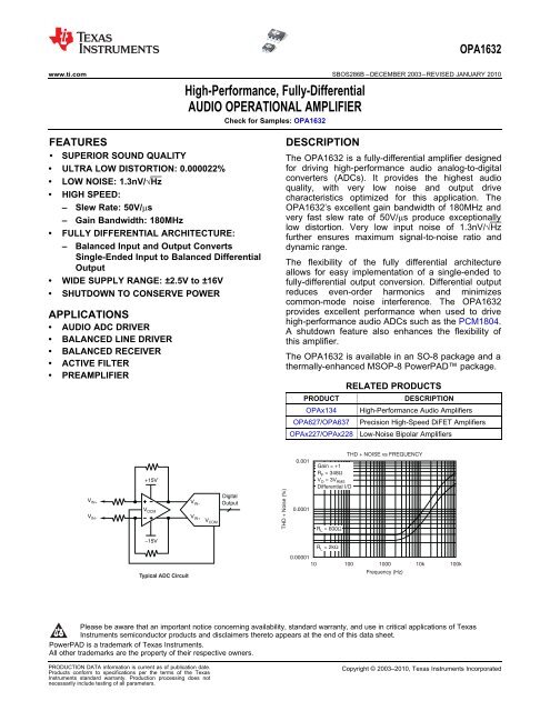
V IN+<br />
V IN<br />
+15V<br />
V OCM<br />
V IN<br />
V IN+<br />
V COM<br />
Digital<br />
Output<br />
THD + Noise (%)<br />
0.001<br />
0.0001<br />
Gain = +1<br />
R F = 348<br />
V O = 3V RMS<br />
<strong>Differential</strong> I/O<br />
RL = 600 <br />
THD + NOISE vs FREQUENCY<br />
15V<br />
Typical ADC Circuit<br />
RL = 2k <br />
0.00001<br />
10 100 1000 10k 100k<br />
Frequency (Hz)<br />
Please be aware that an important notice concerning availability, standard warranty, and use in critical applications of Texas<br />
Instruments semiconductor products and disclaimers thereto appears at the end of this data sheet.<br />
2PowerPAD is a trademark of Texas Instruments.<br />
3All other trademarks are the property of their respective owners.<br />
PRODUCTION DATA information is current as of publication date.<br />
Products conform to specifications per the terms of the Texas<br />
Instruments standard warranty. Production processing does not<br />
necessarily include testing of all parameters.<br />
Copyright © 2003–2010, Texas Instruments Incorporated
OPA1632<br />
SBOS286B –DECEMBER 2003–REVISED JANUARY 2010<br />
www.ti.com<br />
This integrated circuit can be damaged by ESD. Texas Instruments recommends that all integrated circuits be handled with<br />
appropriate precautions. Failure to observe proper handling and installation procedures can cause damage.<br />
ESD damage can range from subtle performance degradation to complete device failure. Precision integrated circuits may be more<br />
susceptible to damage because very small parametric changes could cause the device not to meet its published specifications.<br />
PACKAGE/ORDERING INFORMATION (1)<br />
SPECIFIED<br />
PACKAGE TEMPERATURE PACKAGE TRANSPORT<br />
PRODUCT PACKAGE-LEAD DESIGNATOR RANGE MARKING ORDERING NUMBER MEDIA, QUANTITY<br />
OPA1632<br />
SO-8 D −40°C to +85°C OPA1632<br />
OPA1632D Rails, 100<br />
OPA1632DR Tape and Reel, 2500<br />
MSOP-8<br />
OPA1632DGN Rails, 100<br />
DGK −40°C to +85°C 1632<br />
PowerPAD OPA1632DGNR Tape and Reel, 2500<br />
(1) For the most current package and ordering information see the Package <strong>Op</strong>tion Addendum at the end of this document, or see the TI<br />
web site at www.ti.com.<br />
ABSOLUTE MAXIMUM RATINGS (1)(2)<br />
Over operating free-air temperature range (unless otherwise noted).<br />
OPA1632<br />
Supply Voltage, ±V S ±16.5 V<br />
Input Voltage, V I ±V S V<br />
Output Current, I O 150 mA<br />
<strong>Differential</strong> Input Voltage, V ID ±3 V<br />
Maximum Junction Temperature, T J +150 °C<br />
<strong>Op</strong>erating Free-Air Temperature Range –40 to +85 °C<br />
Storage Temperature Range, T STG –65 to +150 °C<br />
Human Body Model (HBM) 1 kV<br />
ESD Ratings Charged Device Model (CDM) 500 V<br />
Machine Model (MM) 200 V<br />
(1) Stresses above these ratings may cause permanent damage. Exposure to absolute maximum conditions for extended periods may<br />
degrade device reliability. These are stress ratings only, and functional operation of the device at these or any other conditions beyond<br />
those specified is not supported.<br />
(2) The OPA1632 MSOP-8 package version incorporates a PowerPAD on the underside of the chip. This acts as a heatsink and must be<br />
connected to a thermally-dissipative plane for proper power dissipation. Failure to do so may result in exceeding the maximum junction<br />
temperature, which can permanently damage the device. See TI technical brief SLMA002 for more information about using the<br />
PowerPAD thermally-enhanced package.<br />
UNIT<br />
PIN CONFIGURATION<br />
OPA1632<br />
MSOP-8, SO-8<br />
(TOP VIEW)<br />
V IN<br />
1<br />
8<br />
V IN+<br />
V OCM<br />
2<br />
7<br />
Enable<br />
V+<br />
3<br />
6<br />
V<br />
V OUT+<br />
4<br />
5<br />
V OUT<br />
2 Copyright © 2003–2010, Texas Instruments Incorporated<br />
Product Folder Link(s): OPA1632
OPA1632<br />
www.ti.com SBOS286B –DECEMBER 2003–REVISED JANUARY 2010<br />
ELECTRICAL CHARACTERISTICS: V S = ±15V<br />
At V S = ±15V; R F = 390Ω, R L = 800Ω, and G = +1, unless otherwise noted.<br />
OPA1632<br />
PARAMETER CONDITIONS MIN TYP MAX UNIT<br />
OFFSET VOLTAGE<br />
Input Offset Voltage ±0.5 ±3 mV<br />
vs Temperature dV OS /dT ±5 mV°C<br />
vs Power Supply, dc PSRR 316 13 mV/V<br />
INPUT BIAS CURRENT<br />
Input Bias Current I B 2 6 mA<br />
Input Offset Current I OS ±100 ±500 nA<br />
NOISE<br />
Input Voltage Noise f = 10 kHz 1.3 nV/√Hz<br />
Input Current Noise f = 10 kHz 0.4 pA/√Hz<br />
INPUT VOLTAGE<br />
Common-Mode Input Range (V−) + 1.5 (V+) − 1 V<br />
Common-Mode Rejection Ratio, dc 74 90 dB<br />
INPUT IMPEDANCE<br />
Input Impedance (each input pin) 34 || 4 MΩ || pF<br />
OPEN-LOOP GAIN<br />
<strong>Op</strong>en-Loop Gain, dc 66 78 dB<br />
FREQUENCY RESPONSE<br />
Small-Signal Bandwidth G = +1, R F = 348Ω 180 MHz<br />
xxx (V O = 100mV PP , Peaking < 0.5 dB) G = +2, R F = 602Ω 90 MHz<br />
G = +5, R F = 1.5kΩ 36 MHz<br />
G = +10, R F = 3.01kΩ 18 MHz<br />
Bandwidth for 0.1dB Flatness G = +1, V O = 100mV PP 40 MHz<br />
Peaking at a Gain of 1 V O = 100mV PP 0.5 dB<br />
Large-Signal Bandwidth G = +2, V O = 20V PP 800 kHz<br />
Slew Rate (25% to 75% ) G = +1 50 V/ms<br />
Rise and Fall Time G = +1, V O = 5V Step 100 ns<br />
Settling Time to 0.1% G = +1, V O = 2V Step 75 ns<br />
Settling Time to 0.01% G = +1, V O = 2V Step 200 ns<br />
Total Harmonic Distortion + Noise<br />
G = +1, f = 1kHz, V O = 3V RMS<br />
xxx <strong>Differential</strong> Input/Output R L = 600Ω 0.0003 %<br />
xxx <strong>Differential</strong> Input/Output R L = 2kΩ 0.000022 %<br />
xxx Single-Ended In/<strong>Differential</strong> Out R L = 600Ω 0.000059 %<br />
xxx Single-Ended In/<strong>Differential</strong> Out R L = 2kΩ 0.000043 %<br />
Intermodulation Distortion<br />
G = +1, SMPTE/DIN, V O = 2V PP<br />
xxx <strong>Differential</strong> Input/Output R L = 600Ω 0.00008 %<br />
xxx <strong>Differential</strong> Input/Output R L = 2kΩ 0.00005 %<br />
xxx Single-Ended In/<strong>Differential</strong> Out R L = 600Ω 0.0001 %<br />
xxx Single-Ended In/<strong>Differential</strong> Out R L = 2kΩ 0.0007 %<br />
Headroom THD < 0.01%, R L = 2kΩ 20.0 V PP<br />
OUTPUT<br />
Voltage Output Swing R L = 2kΩ (V+) − 1.9 (V−) + 1.9 V<br />
R L = 800Ω (V+) − 4.5 (V−) + 4.5 V<br />
Short-Circuit Current I SC Sourcing/Sinking +50/−60 85 mA<br />
Closed-Loop Output Impedance G = +1, f = 100kHz 0.3 Ω<br />
Copyright © 2003–2010, Texas Instruments Incorporated 3<br />
Product Folder Link(s): OPA1632
OPA1632<br />
SBOS286B –DECEMBER 2003–REVISED JANUARY 2010<br />
www.ti.com<br />
ELECTRICAL CHARACTERISTICS: V S = ±15V (continued)<br />
At V S = ±15V; R F = 390Ω, R L = 800Ω, and G = +1, unless otherwise noted.<br />
POWER-DOWN (1)<br />
OPA1632<br />
PARAMETER CONDITIONS MIN TYP MAX UNIT<br />
Enable Voltage Threshold (V−) + 2 V<br />
Disable Voltage Threshold (V−) + 0.8 V<br />
Shutdown Current V ENABLE = −15V 0.85 mA<br />
Turn-On Delay Time for I Q to Reach 50% 2 ms<br />
Turn-Off Delay Time for I Q to Reach 50% 2 ms<br />
POWER SUPPLY<br />
Specified <strong>Op</strong>erating Voltage ±15 ±16 V<br />
<strong>Op</strong>erating Voltage ±2.5 V<br />
Quiescent Current I Q Per Channel 14 17.1 mA<br />
TEMPERATURE RANGE<br />
Specified Range –40 +85 °C<br />
<strong>Op</strong>erating Range –40 +125 °C<br />
Storage Range –65 +150 °C<br />
Thermal Resistance<br />
q JA<br />
SO-8, MSOP-8 200 °C/W<br />
(1) <strong>Amp</strong>lifier has internal 50kΩ pull-up resistor to V CC + pin. This enables the amplifier with no connection to shutdown pin.<br />
4 Copyright © 2003–2010, Texas Instruments Incorporated<br />
Product Folder Link(s): OPA1632
OPA1632<br />
www.ti.com SBOS286B –DECEMBER 2003–REVISED JANUARY 2010<br />
TYPICAL CHARACTERISTICS<br />
At T A = +25°C, V S = ±15V, and R L = 2kΩ, unless otherwise noted.<br />
THD + NOISE vs FREQUENCY<br />
THD + NOISE vs FREQUENCY<br />
THD + Noise (%)<br />
0.001<br />
0.0001<br />
Gain = +1<br />
R F = 348<br />
V O = 3VRMS<br />
<strong>Differential</strong> I/O<br />
R = 600<br />
L<br />
THD + Noise (%)<br />
0.001<br />
0.0001<br />
Gain = +1<br />
R<br />
F<br />
= 348<br />
V<br />
O<br />
= 3VRMS<br />
Single-Ended Input<br />
<strong>Differential</strong> Output<br />
RL = 600 <br />
RL = 2k <br />
R = 2k<br />
L<br />
0.00001<br />
10 100 1k 10k 100k<br />
Frequency (Hz)<br />
0.00001<br />
10 100 1k 10k 100k<br />
Figure 1. Figure 2.<br />
Frequency (Hz)<br />
THD + Noise (%)<br />
0.1<br />
0.01<br />
0.001<br />
0.0001<br />
THD + NOISE vs OUTPUT VOLTAGE<br />
Gain = +1<br />
R F = 348<br />
f = 1kHz<br />
<strong>Differential</strong> I/O<br />
0.00001<br />
0.01 0.1 1 10 100<br />
<strong>Differential</strong> Output V oltage (V RMS<br />
)<br />
R<br />
<br />
L = 600 R <br />
L = 2k<br />
THD + Noise (%)<br />
0.01<br />
0.001<br />
THD + NOISE vs OUTPUT VOLTAGE<br />
R = 600<br />
L<br />
0.0001 Gain = +1<br />
R F<br />
= 348<br />
R<br />
L<br />
= 2k<br />
f = 1kHz<br />
Single-Ended Input<br />
<strong>Differential</strong> Output<br />
0.00001<br />
0.01 0.1 1 10 100<br />
Figure 3. Figure 4.<br />
<strong>Differential</strong> Output Voltage (V )<br />
RMS<br />
0.1<br />
INTERMODULATION DISTORTION<br />
vs OUTPUT VOLTAGE<br />
0.1<br />
INTERMODULATION DISTORTION<br />
vs OUTPUT VOLTAGE<br />
0.01<br />
0.01<br />
IMD (%)<br />
0.001<br />
Gain = +1<br />
0.0001<br />
R F<br />
= 348<br />
<strong>Differential</strong> I/O<br />
SMPTE 4:1; 60Hz, 7kHz<br />
R<br />
L<br />
= 2k<br />
DIN 4:1; 250Hz, 8kHz<br />
0.00001<br />
0.01 0.1 1 10 100<br />
<strong>Differential</strong> Output Voltage (V PP<br />
)<br />
R = 600<br />
L<br />
RL = 600 <br />
0.001<br />
Gain = +1<br />
R F<br />
= 348<br />
RL Single-Ended Input<br />
= 2k <br />
0.0001<br />
<strong>Differential</strong> Output<br />
SMPTE 4:1; 60Hz, 7kHz<br />
DIN 4:1; 250Hz, 8kHz<br />
0.00001<br />
0.01 0.1 1 10 100<br />
IMD (%)<br />
<strong>Differential</strong> Output Voltage (V PP<br />
)<br />
Figure 5. Figure 6.<br />
Copyright © 2003–2010, Texas Instruments Incorporated 5<br />
Product Folder Link(s): OPA1632
OPA1632<br />
SBOS286B –DECEMBER 2003–REVISED JANUARY 2010<br />
www.ti.com<br />
TYPICAL CHARACTERISTICS (continued)<br />
At T A = +25°C, V S = ±15V, and R L = 2kΩ, unless otherwise noted.<br />
VOLTAGE NOISE vs FREQUENCY<br />
CURRENT NOISE vs FREQUENCY<br />
10<br />
10<br />
V<br />
n<br />
(nV/ Hz )<br />
I<br />
n<br />
(pA/ Hz )<br />
1<br />
1<br />
0.1<br />
10 100 1k 10k 100k<br />
10 100 1k 10k 100k<br />
Frequency (Hz)<br />
Frequency (Hz)<br />
Figure 7. Figure 8.<br />
15<br />
10<br />
OUTPUT VOLTAGE<br />
vs DIFFERENTIAL LOAD RESISTANCE<br />
R F<br />
= 1k<br />
G = +2<br />
V CC<br />
= 15V<br />
100<br />
V CC<br />
= 5V<br />
OUTPUT IMPEDANCE<br />
vs FREQUENCY<br />
V (V)<br />
O<br />
5<br />
0<br />
5<br />
10<br />
15<br />
100 1k 10k 100k<br />
R L<br />
()<br />
V CC<br />
= 5V<br />
V CC<br />
= 5V<br />
V CC<br />
= 15V<br />
Output Impedance ( )<br />
10<br />
1<br />
0.1<br />
100k 1M 10M 100M 1G<br />
Frequency (Hz)<br />
Figure 9. Figure 10.<br />
6 Copyright © 2003–2010, Texas Instruments Incorporated<br />
Product Folder Link(s): OPA1632
OPA1632<br />
www.ti.com SBOS286B –DECEMBER 2003–REVISED JANUARY 2010<br />
APPLICATION INFORMATION<br />
Figure 11 shows the OPA1632 used as a The V COM reference voltage output on the PCM1804<br />
differential-output driver for the PCM1804 ADC provides the proper input common-mode<br />
high-performance audio ADC. reference voltage (2.5V). This V COM voltage is<br />
buffered with op amp A 2 and drives the output<br />
Supply voltages of ±15V are commonly used for the<br />
common-mode voltage pin of the OPA1632. This<br />
OPA1632. The relatively low input voltage swing<br />
biases the average output voltage of the OPA1632 to<br />
required by the ADC allows use of lower<br />
2.5V.<br />
power-supply voltage, if desired. Power supplies as<br />
low as ±8V can be used in this application with The signal gain of the circuit is generally set to<br />
excellent performance. This reduces power approximately 0.25 to be compatible with<br />
dissipation and heat rise. Power supplies should be commonly-used audio line levels. Gain can be<br />
bypassed with 10mF tantalum capacitors in parallel adjusted, if necessary, by changing the values of R 1<br />
with 0.1mF ceramic capacitors to avoid possible and R 2 . The feedback resistor values (R 3 and R 4 )<br />
oscillations and instability.<br />
should be kept relatively low, as indicated, for best<br />
noise performance.<br />
R 5 , R 6 , and C 3 provide an input filter and charge<br />
glitch reservoir for the ADC. The values shown are<br />
generally satisfactory. Some adjustment of the values<br />
may help optimize performance with different ADCs.<br />
V+<br />
+8V to +16V<br />
10F<br />
+<br />
0.1F<br />
R 3<br />
270<br />
C 1<br />
1nF<br />
Balanced or<br />
Single- Ended<br />
Input<br />
+<br />
<br />
R 1<br />
1k<br />
R 2<br />
1k<br />
8<br />
3<br />
V OCM<br />
2<br />
1<br />
7<br />
6<br />
5<br />
OPA1632<br />
4<br />
C 2<br />
1nF<br />
R 5<br />
40<br />
R 6<br />
40<br />
C 3<br />
2.7nF<br />
1/2<br />
PCM1804<br />
V COM<br />
(2.5V)<br />
R 4<br />
270<br />
Enable (1)<br />
0.1F<br />
OPA134<br />
1k<br />
0.1F<br />
10F<br />
+<br />
8V to 16V<br />
V<br />
Figure 11. ADC Driver for Professional <strong>Audio</strong><br />
Copyright © 2003–2010, Texas Instruments Incorporated 7<br />
Product Folder Link(s): OPA1632
OPA1632<br />
SBOS286B –DECEMBER 2003–REVISED JANUARY 2010<br />
www.ti.com<br />
It is important to maintain accurate resistor matching SHUTDOWN FUNCTION<br />
on R 1 /R 2 and R 3 /R 4 to achieve good differential signal<br />
balance. Use 1% resistors for highest performance.<br />
The shutdown (enable) function of the OPA1632 is<br />
When connected for single-ended inputs (inverting<br />
referenced to the negative supply of the operational<br />
input grounded, as shown in Figure 11), the source<br />
amplifier. A valid logic low (< 0.8V above negative<br />
impedance must be low. <strong>Differential</strong> input sources<br />
supply) applied to the enable pin (pin 7) disables the<br />
must have well-balanced or low source impedance.<br />
amplifier output. Voltages applied to pin 7 that are<br />
greater than 2V above the negative supply place the<br />
Capacitors C 1 , C 2 , and C 3 should be chosen carefully amplifier output in an active state, and the device is<br />
for good distortion performance. Polystyrene, enabled. If pin 7 is left disconnected, an internal<br />
polypropylene, NPO ceramic, and mica types are pull-up resistor enables the device. Turn-on and<br />
generally excellent. Polyester and high-K ceramic turn-off times are approximately 2ms each.<br />
types such as Z5U can create distortion.<br />
Quiescent current is reduced to approximately<br />
0.85mA when the amplifier is disabled. When<br />
FULLY-DIFFERENTIAL AMPLIFIERS<br />
disabled, the output stage is not in a high-impedance<br />
<strong>Differential</strong> signal processing offers a number of state. Thus, the shutdown function cannot be used to<br />
performance advantages in high-speed analog signal create a multiplexed switching function in series with<br />
processing systems, including immunity to external multiple amplifiers.<br />
common-mode noise, suppression of even-order<br />
nonlinearities, and increased dynamic range. OUTPUT COMMON-MODE VOLTAGE<br />
<strong>Fully</strong>-differential amplifiers not only serve as the<br />
primary means of providing gain to a differential<br />
The output common-mode voltage pin sets the dc<br />
signal chain, but also provide a monolithic solution for<br />
output voltage of the OPA1632. A voltage applied to<br />
converting single-ended signals into differential<br />
the V OCM pin from a low-impedance source can be<br />
signals allowing for easy, high-performance<br />
used to directly set the output common-mode voltage.<br />
processing.<br />
For a V OCM voltage at mid-supply, make no<br />
connection to the V OCM pin.<br />
A standard configuration for the device is shown in<br />
Figure 12. The functionality of a fully differential<br />
Depending on the intended application, a decoupling<br />
amplifier can be imagined as two inverting amplifiers<br />
capacitor is recommended on the V OCM node to filter<br />
that share a common noninverting terminal (though<br />
any high-frequency noise that could couple into the<br />
the voltage is not necessarily fixed). For more<br />
signal path through the V OCM circuitry. A 0.1mF or 1mF<br />
information on the basic theory of operation for fully<br />
capacitor is generally adequate.<br />
differential amplifiers, refer to the Texas Instruments Output common-mode voltage causes additional<br />
application note SLOA054, <strong>Fully</strong> <strong>Differential</strong> current to flow in the feedback resistor network. Since<br />
<strong>Amp</strong>lifiers, available for download from the TI web this current is supplied by the output stage of the<br />
site (www.ti.com).<br />
amplifier, this creates additional power dissipation.<br />
For commonly-used feedback resistance values, this<br />
current is easily supplied by the amplifier. The<br />
additional internal power dissipation created by this<br />
+15V<br />
current may be significant in some applications and<br />
may dictate use of the MSOP PowerPAD package to<br />
effectively control self-heating.<br />
V IN+<br />
V OCM<br />
V IN<br />
Digital<br />
Output<br />
V IN<br />
V IN+<br />
V COM<br />
15V<br />
Figure 12. Typical ADC Circuit<br />
8 Copyright © 2003–2010, Texas Instruments Incorporated<br />
Product Folder Link(s): OPA1632
OPA1632<br />
www.ti.com SBOS286B –DECEMBER 2003–REVISED JANUARY 2010<br />
PowerPAD DESIGN CONSIDERATIONS<br />
3. Place five holes in the area of the thermal pad.<br />
These holes should be 13mils (0,03302cm) in<br />
The OPA1632 is available in a thermally-enhanced<br />
diameter. Keep them small so that solder wicking<br />
PowerPAD family of packages. These packages are<br />
through the holes is not a problem during reflow.<br />
constructed using a downset leadframe upon which<br />
the die is mounted (see Figure 13[a] and 4. Additional vias may be placed anywhere along<br />
Figure 13[b]). This arrangement results in the lead the thermal plane outside of the thermal pad<br />
frame being exposed as a thermal pad on the area. These vias help dissipate the heat<br />
underside of the package (see Figure 13[c]). Because generated by the OPA1632 IC, and may be larger<br />
this thermal pad has direct thermal contact with the than the 13mil diameter vias directly under the<br />
die, excellent thermal performance can be achieved thermal pad. They can be larger because they<br />
by providing a good thermal path away from the are not in the thermal pad area to be soldered so<br />
thermal pad.<br />
that wicking is not a problem.<br />
5. Connect all holes to the internal ground plane.<br />
6. When connecting these holes to the plane, do not<br />
DIE<br />
use the typical web or spoke via connection<br />
methodology. Web connections have a high<br />
(a) Side View<br />
Thermal<br />
thermal resistance connection that is useful for<br />
Pad<br />
slowing the heat transfer during soldering<br />
DIE<br />
operations. This makes the soldering of vias that<br />
(b) End View<br />
(c) Bottom View<br />
have plane connections easier. In this application,<br />
however, low thermal resistance is desired for the<br />
most efficient heat transfer. Therefore, the holes<br />
Figure 13. Views of the Thermally-Enhanced<br />
under the OPA1632 PowerPAD package should<br />
Package<br />
make their connection to the internal plane with a<br />
complete connection around the entire<br />
The PowerPAD package allows for both assembly circumference of the plated-through hole.<br />
and thermal management in one manufacturing 7. The top-side solder mask should leave the<br />
operation. During the surface-mount solder operation terminals of the package and the thermal pad<br />
(when the leads are being soldered), the thermal pad area with its five holes exposed. The bottom-side<br />
must be soldered to a copper area underneath the solder mask should cover the five holes of the<br />
package. Through the use of thermal paths within this thermal pad area. This prevents solder from<br />
copper area, heat can be conducted away from the being pulled away from the thermal pad area<br />
package into either a ground plane or other during the reflow process.<br />
heat-dissipating device. Soldering the PowerPAD to 8. Apply solder paste to the exposed thermal pad<br />
the printed circuit board (PCB) is always required, area and all of the IC terminals.<br />
even with applications that have low power<br />
dissipation. It provides the necessary thermal and With these preparatory steps in place, the IC is<br />
mechanical connection between the lead frame die simply placed in position and runs through the<br />
pad and the PCB.<br />
solder reflow operation as any standard<br />
surface-mount component. This results in a part<br />
that is properly installed.<br />
PowerPAD PCB LAYOUT CONSIDERATIONS<br />
1. The PowerPAD is electrically isolated from the<br />
silicon and all leads. Connecting the PowerPAD<br />
to any potential voltage between the<br />
power-supply voltages is acceptable, but it is<br />
recommended to tie to ground because it is<br />
generally the largest conductive plane.<br />
2. Prepare the PCB with a top-side etch pattern, as<br />
shown in Figure 14. There should be etch for the<br />
leads as well as etch for the thermal pad.<br />
space<br />
Single or Dual<br />
68mils 70mils (0,1727cm 0,1778cm)<br />
(via diameter = 13mils (0,03302cm)<br />
Figure 14. PowerPAD PCB Etch and Via Pattern<br />
Copyright © 2003–2010, Texas Instruments Incorporated 9<br />
Product Folder Link(s): OPA1632
OPA1632<br />
SBOS286B –DECEMBER 2003–REVISED JANUARY 2010<br />
www.ti.com<br />
POWER DISSIPATION AND THERMAL<br />
For systems where heat dissipation is more critical,<br />
CONSIDERATIONS the OPA1632 is offered in an MSOP-8 with<br />
PowerPAD. The thermal coefficient for the MSOP<br />
The OPA1632 does not have thermal shutdown<br />
PowerPAD (DGN) package is substantially improved<br />
protection. Take care to assure that the maximum<br />
over the traditional SO package. Maximum power<br />
junction temperature is not exceeded. Excessive<br />
dissipation levels are depicted in Figure 15 for the<br />
junction temperature can degrade performance or<br />
two packages. The data for the DGN package<br />
cause permanent damage. For best performance and<br />
assume a board layout that follows the PowerPAD<br />
reliability, assure that the junction temperature does<br />
layout guidelines.<br />
not exceed +125°C.<br />
The thermal characteristics of the device are dictated<br />
by the package and the circuit board. Maximum<br />
power dissipation for a given package can be<br />
calculated using the following formula:<br />
TMax<br />
TA<br />
P<br />
DMax<br />
=<br />
<br />
JA<br />
where:<br />
• P DMax is the maximum power dissipation in the<br />
amplifier (W)<br />
• T Max is the absolute maximum junction<br />
temperature (°C)<br />
• T A is the ambient temperature (°C)<br />
• q JA = q JC + q CA<br />
• q JC is the thermal coefficient from the silicon<br />
junctions to the case (°C/W)<br />
Maximum Power Dissipation (W)<br />
3.5<br />
3.0<br />
2.5<br />
2.0<br />
1.5<br />
1.0<br />
0.5<br />
SO-8 (D) Package<br />
MAXIMUM POWER DISSIPATION<br />
vs AMBIENT TEMPERATURE<br />
MSOP-8 (DGN) Package<br />
JA<br />
= 170C/W for SO-8 (D)<br />
JA<br />
= 58.4C/W for MSOP-8 (DGN)<br />
T J<br />
= +150C<br />
No Airflow<br />
0<br />
40 15 10 35 60 85<br />
Ambient Temperature ( C)<br />
Figure 15. Maximum Power Dissipation vs<br />
• q CA is the thermal coefficient from the case to Ambient Temperature<br />
ambient air (°C/W)<br />
space<br />
REVISION HISTORY<br />
NOTE: Page numbers for previous revisions may differ from page numbers in the current version.<br />
Changes from <strong>Rev</strong>ision A (September, 2006) to <strong>Rev</strong>ision B<br />
Page<br />
• Updated document format to align with current standards ................................................................................................... 1<br />
• Changed points 1 and 5 of PowerPAD PCB Layout Considerations section ....................................................................... 9<br />
10 Copyright © 2003–2010, Texas Instruments Incorporated<br />
Product Folder Link(s): OPA1632
PACKAGE OPTION ADDENDUM<br />
www.ti.com<br />
14-Aug-2009<br />
PACKAGING INFORMATION<br />
Orderable Device Status (1) Package<br />
Type<br />
Package<br />
Drawing<br />
Pins Package<br />
Qty<br />
OPA1632D ACTIVE SOIC D 8 75 Green (RoHS &<br />
no Sb/Br)<br />
OPA1632DG4 ACTIVE SOIC D 8 75 Green (RoHS &<br />
no Sb/Br)<br />
OPA1632DGN ACTIVE MSOP-<br />
Power<br />
PAD<br />
OPA1632DGNG4 ACTIVE MSOP-<br />
Power<br />
PAD<br />
OPA1632DGNR ACTIVE MSOP-<br />
Power<br />
PAD<br />
OPA1632DGNRG4 ACTIVE MSOP-<br />
Power<br />
PAD<br />
DGN 8 80 Green (RoHS &<br />
no Sb/Br)<br />
DGN 8 80 Green (RoHS &<br />
no Sb/Br)<br />
DGN 8 2500 Green (RoHS &<br />
no Sb/Br)<br />
DGN 8 2500 Green (RoHS &<br />
no Sb/Br)<br />
OPA1632DR ACTIVE SOIC D 8 2500 Green (RoHS &<br />
no Sb/Br)<br />
OPA1632DRG4 ACTIVE SOIC D 8 2500 Green (RoHS &<br />
no Sb/Br)<br />
Eco Plan (2) Lead/Ball Finish MSL Peak Temp (3)<br />
CU NIPDAU<br />
CU NIPDAU<br />
CU NIPDAU<br />
CU NIPDAU<br />
CU NIPDAU<br />
CU NIPDAU<br />
CU NIPDAU<br />
CU NIPDAU<br />
Level-1-260C-UNLIM<br />
Level-1-260C-UNLIM<br />
Level-1-260C-UNLIM<br />
Level-1-260C-UNLIM<br />
Level-1-260C-UNLIM<br />
Level-1-260C-UNLIM<br />
Level-1-260C-UNLIM<br />
Level-1-260C-UNLIM<br />
(1) The marketing status values are defined as follows:<br />
ACTIVE: Product device recommended for new designs.<br />
LIFEBUY: TI has announced that the device will be discontinued, and a lifetime-buy period is in effect.<br />
NRND: Not recommended for new designs. Device is in production to support existing customers, but TI does not recommend using this part in<br />
a new design.<br />
PREVIEW: Device has been announced but is not in production. Samples may or may not be available.<br />
OBSOLETE: TI has discontinued the production of the device.<br />
(2) Eco Plan - The planned eco-friendly classification: Pb-Free (RoHS), Pb-Free (RoHS Exempt), or Green (RoHS & no Sb/Br) - please check<br />
http://www.ti.com/productcontent for the latest availability information and additional product content details.<br />
TBD: The Pb-Free/Green conversion plan has not been defined.<br />
Pb-Free (RoHS): TI's terms "Lead-Free" or "Pb-Free" mean semiconductor products that are compatible with the current RoHS requirements<br />
for all 6 substances, including the requirement that lead not exceed 0.1% by weight in homogeneous materials. Where designed to be soldered<br />
at high temperatures, TI Pb-Free products are suitable for use in specified lead-free processes.<br />
Pb-Free (RoHS Exempt): This component has a RoHS exemption for either 1) lead-based flip-chip solder bumps used between the die and<br />
package, or 2) lead-based die adhesive used between the die and leadframe. The component is otherwise considered Pb-Free (RoHS<br />
compatible) as defined above.<br />
Green (RoHS & no Sb/Br): TI defines "Green" to mean Pb-Free (RoHS compatible), and free of Bromine (Br) and Antimony (Sb) based flame<br />
retardants (Br or Sb do not exceed 0.1% by weight in homogeneous material)<br />
(3)<br />
MSL, Peak Temp. -- The Moisture Sensitivity Level rating according to the JEDEC industry standard classifications, and peak solder<br />
temperature.<br />
Important Information and Disclaimer:The information provided on this page represents TI's knowledge and belief as of the date that it is<br />
provided. TI bases its knowledge and belief on information provided by third parties, and makes no representation or warranty as to the<br />
accuracy of such information. Efforts are underway to better integrate information from third parties. TI has taken and continues to take<br />
reasonable steps to provide representative and accurate information but may not have conducted destructive testing or chemical analysis on<br />
incoming materials and chemicals. TI and TI suppliers consider certain information to be proprietary, and thus CAS numbers and other limited<br />
information may not be available for release.<br />
In no event shall TI's liability arising out of such information exceed the total purchase price of the TI part(s) at issue in this document sold by TI<br />
to Customer on an annual basis.<br />
Addendum-Page 1
PACKAGE MATERIALS INFORMATION<br />
www.ti.com<br />
5-Feb-2011<br />
TAPE AND REEL INFORMATION<br />
*All dimensions are nominal<br />
Device<br />
OPA1632DGNR<br />
Package<br />
Type<br />
MSOP-<br />
Power<br />
PAD<br />
Package<br />
Drawing<br />
Pins SPQ Reel<br />
Diameter<br />
(mm)<br />
Reel<br />
Width<br />
W1 (mm)<br />
A0<br />
(mm)<br />
B0<br />
(mm)<br />
K0<br />
(mm)<br />
P1<br />
(mm)<br />
W<br />
(mm)<br />
Pin1<br />
Quadrant<br />
DGN 8 2500 330.0 12.4 5.3 3.4 1.4 8.0 12.0 Q1<br />
OPA1632DR SOIC D 8 2500 330.0 12.4 6.4 5.2 2.1 8.0 12.0 Q1<br />
Pack Materials-Page 1
PACKAGE MATERIALS INFORMATION<br />
www.ti.com<br />
5-Feb-2011<br />
*All dimensions are nominal<br />
Device Package Type Package Drawing Pins SPQ Length (mm) Width (mm) Height (mm)<br />
OPA1632DGNR MSOP-PowerPAD DGN 8 2500 358.0 335.0 35.0<br />
OPA1632DR SOIC D 8 2500 346.0 346.0 29.0<br />
Pack Materials-Page 2
IMPORTANT NOTICE<br />
Texas Instruments Incorporated and its subsidiaries (TI) reserve the right to make corrections, modifications, enhancements, improvements,<br />
and other changes to its products and services at any time and to discontinue any product or service without notice. Customers should<br />
obtain the latest relevant information before placing orders and should verify that such information is current and complete. All products are<br />
sold subject to TI’s terms and conditions of sale supplied at the time of order acknowledgment.<br />
TI warrants performance of its hardware products to the specifications applicable at the time of sale in accordance with TI’s standard<br />
warranty. Testing and other quality control techniques are used to the extent TI deems necessary to support this warranty. Except where<br />
mandated by government requirements, testing of all parameters of each product is not necessarily performed.<br />
TI assumes no liability for applications assistance or customer product design. Customers are responsible for their products and<br />
applications using TI components. To minimize the risks associated with customer products and applications, customers should provide<br />
adequate design and operating safeguards.<br />
TI does not warrant or represent that any license, either express or implied, is granted under any TI patent right, copyright, mask work right,<br />
or other TI intellectual property right relating to any combination, machine, or process in which TI products or services are used. Information<br />
published by TI regarding third-party products or services does not constitute a license from TI to use such products or services or a<br />
warranty or endorsement thereof. Use of such information may require a license from a third party under the patents or other intellectual<br />
property of the third party, or a license from TI under the patents or other intellectual property of TI.<br />
Reproduction of TI information in TI data books or data sheets is permissible only if reproduction is without alteration and is accompanied<br />
by all associated warranties, conditions, limitations, and notices. Reproduction of this information with alteration is an unfair and deceptive<br />
business practice. TI is not responsible or liable for such altered documentation. Information of third parties may be subject to additional<br />
restrictions.<br />
Resale of TI products or services with statements different from or beyond the parameters stated by TI for that product or service voids all<br />
express and any implied warranties for the associated TI product or service and is an unfair and deceptive business practice. TI is not<br />
responsible or liable for any such statements.<br />
TI products are not authorized for use in safety-critical applications (such as life support) where a failure of the TI product would reasonably<br />
be expected to cause severe personal injury or death, unless officers of the parties have executed an agreement specifically governing<br />
such use. Buyers represent that they have all necessary expertise in the safety and regulatory ramifications of their applications, and<br />
acknowledge and agree that they are solely responsible for all legal, regulatory and safety-related requirements concerning their products<br />
and any use of TI products in such safety-critical applications, notwithstanding any applications-related information or support that may be<br />
provided by TI. Further, Buyers must fully indemnify TI and its representatives against any damages arising out of the use of TI products in<br />
such safety-critical applications.<br />
TI products are neither designed nor intended for use in military/aerospace applications or environments unless the TI products are<br />
specifically designated by TI as military-grade or "enhanced plastic." Only products designated by TI as military-grade meet military<br />
specifications. Buyers acknowledge and agree that any such use of TI products which TI has not designated as military-grade is solely at<br />
the Buyer's risk, and that they are solely responsible for compliance with all legal and regulatory requirements in connection with such use.<br />
TI products are neither designed nor intended for use in automotive applications or environments unless the specific TI products are<br />
designated by TI as compliant with ISO/TS 16949 requirements. Buyers acknowledge and agree that, if they use any non-designated<br />
products in automotive applications, TI will not be responsible for any failure to meet such requirements.<br />
Following are URLs where you can obtain information on other Texas Instruments products and application solutions:<br />
Products<br />
Applications<br />
<strong>Audio</strong> www.ti.com/audio Communications and Telecom www.ti.com/communications<br />
<strong>Amp</strong>lifiers amplifier.ti.com Computers and Peripherals www.ti.com/computers<br />
Data Converters dataconverter.ti.com Consumer Electronics www.ti.com/consumer-apps<br />
DLP® Products www.dlp.com Energy and Lighting www.ti.com/energy<br />
DSP dsp.ti.com Industrial www.ti.com/industrial<br />
Clocks and Timers www.ti.com/clocks Medical www.ti.com/medical<br />
Interface interface.ti.com Security www.ti.com/security<br />
Logic logic.ti.com Space, Avionics and Defense www.ti.com/space-avionics-defense<br />
Power Mgmt power.ti.com Transportation and www.ti.com/automotive<br />
Automotive<br />
Microcontrollers microcontroller.ti.com Video and Imaging www.ti.com/video<br />
RFID www.ti-rfid.com Wireless www.ti.com/wireless-apps<br />
RF/IF and ZigBee® Solutions<br />
www.ti.com/lprf<br />
TI E2E Community Home Page<br />
e2e.ti.com<br />
Mailing Address: Texas Instruments, Post Office Box 655303, Dallas, Texas 75265<br />
Copyright © 2011, Texas Instruments Incorporated