Lecture 1 - Webstaff.kmutt.ac.th - kmutt
Lecture 1 - Webstaff.kmutt.ac.th - kmutt
Lecture 1 - Webstaff.kmutt.ac.th - kmutt

Create successful ePaper yourself
Turn your PDF publications into a flip-book with our unique Google optimized e-Paper software.
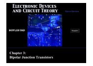
Chapter 1:<br />
Semiconductor Diodes<br />
© Modified by Yuttapong Jiraraksopakun<br />
ENE, KMUTT 2009
Semiconductors, Insulators, Conductors<br />
Electronic Devices and Circuit Theory, 10/e<br />
Robert L. Boylestad and Louis Nashelsky<br />
2<br />
Copyright ©2009 by Pearson Education, Inc.<br />
Upper Saddle River, New Jersey 07458 • All rights reserved.
Semiconductor Materials<br />
Materials commonly used in <strong>th</strong>e development of<br />
semiconductor devices:<br />
• Silicon (Si)<br />
• Germanium (Ge)<br />
• Gallium Arsenide (GaAs)<br />
Electronic Devices and Circuit Theory, 10/e<br />
Robert L. Boylestad and Louis Nashelsky<br />
3<br />
Copyright ©2009 by Pearson Education, Inc.<br />
Upper Saddle River, New Jersey 07458 • All rights reserved.
Conduction in Semiconductors<br />
Electronic Devices and Circuit Theory, 10/e<br />
Robert L. Boylestad and Louis Nashelsky<br />
4<br />
Copyright ©2009 by Pearson Education, Inc.<br />
Upper Saddle River, New Jersey 07458 • All rights reserved.
Doping<br />
The electrical char<strong>ac</strong>teristics of silicon and germanium are improved<br />
by adding materials in a process called doping.<br />
There are just two types of doped semiconductor materials:<br />
n-type<br />
p-type<br />
• n-type materials contain an excess of conduction band electrons.<br />
• p-type materials contain an excess of valence band holes.<br />
Electronic Devices and Circuit Theory, 10/e<br />
Robert L. Boylestad and Louis Nashelsky<br />
5<br />
Copyright ©2009 by Pearson Education, Inc.<br />
Upper Saddle River, New Jersey 07458 • All rights reserved.
Majority and Minority Carriers<br />
Two currents <strong>th</strong>rough a diode:<br />
Majority Carriers<br />
• The majority carriers in n-type materials are electrons.<br />
• The majority carriers in p-type materials are holes.<br />
Minority Carriers<br />
• The minority carriers in n-type materials are holes.<br />
• The minority carriers in p-type materials are electrons.<br />
Electronic Devices and Circuit Theory, 10/e<br />
Robert L. Boylestad and Louis Nashelsky<br />
6<br />
Copyright ©2009 by Pearson Education, Inc.<br />
Upper Saddle River, New Jersey 07458 • All rights reserved.
p-n Junctions<br />
One end of a silicon or germanium crystal can be doped as a p-<br />
type material and <strong>th</strong>e o<strong>th</strong>er end as an n-type material.<br />
The result is a p-n junction.<br />
Electronic Devices and Circuit Theory, 10/e<br />
Robert L. Boylestad and Louis Nashelsky<br />
7<br />
Copyright ©2009 by Pearson Education, Inc.<br />
Upper Saddle River, New Jersey 07458 • All rights reserved.
At <strong>th</strong>e p-n junction, <strong>th</strong>e excess<br />
conduction-band electrons on <strong>th</strong>e<br />
n-type side are attr<strong>ac</strong>ted to <strong>th</strong>e<br />
valence-band holes on <strong>th</strong>e p-type<br />
side.<br />
p-n Junctions<br />
The electrons in <strong>th</strong>e n-type<br />
material migrate <strong>ac</strong>ross <strong>th</strong>e<br />
junction to <strong>th</strong>e p-type material<br />
(electron flow).<br />
The result is <strong>th</strong>e formation of a<br />
depletion region around <strong>th</strong>e<br />
junction.<br />
The electron migration results in<br />
a negative charge on <strong>th</strong>e p-type<br />
side of <strong>th</strong>e junction and a positive<br />
charge on <strong>th</strong>e n-type side of <strong>th</strong>e<br />
junction.<br />
Electronic Devices and Circuit Theory, 10/e<br />
Robert L. Boylestad and Louis Nashelsky<br />
8<br />
Copyright ©2009 by Pearson Education, Inc.<br />
Upper Saddle River, New Jersey 07458 • All rights reserved.
Diodes<br />
The diode is a 2-terminal device.<br />
A diode ideally conducts in<br />
only one direction.<br />
Electronic Devices and Circuit Theory, 10/e<br />
Robert L. Boylestad and Louis Nashelsky<br />
9<br />
Copyright ©2009 by Pearson Education, Inc.<br />
Upper Saddle River, New Jersey 07458 • All rights reserved.
Diode Operating Conditions<br />
A diode has <strong>th</strong>ree operating conditions:<br />
• No bias<br />
• Forward bias<br />
• Reverse bias<br />
Electronic Devices and Circuit Theory, 10/e<br />
Robert L. Boylestad and Louis Nashelsky<br />
10<br />
Copyright ©2009 by Pearson Education, Inc.<br />
Upper Saddle River, New Jersey 07458 • All rights reserved.
Diode Operating Conditions<br />
No Bias<br />
• No external voltage is applied: V D = 0 V<br />
• No current is flowing: I D = 0 A<br />
• Only a modest depletion region exists<br />
Electronic Devices and Circuit Theory, 10/e<br />
Robert L. Boylestad and Louis Nashelsky<br />
11<br />
Copyright ©2009 by Pearson Education, Inc.<br />
Upper Saddle River, New Jersey 07458 • All rights reserved.
Reverse Bias<br />
Diode Operating Conditions<br />
External voltage is applied <strong>ac</strong>ross <strong>th</strong>e p-n junction in<br />
<strong>th</strong>e opposite polarity of <strong>th</strong>e p- and n-type materials.<br />
• The reverse voltage causes <strong>th</strong>e<br />
depletion region to widen.<br />
• The electrons in <strong>th</strong>e n-type material<br />
are attr<strong>ac</strong>ted toward <strong>th</strong>e positive<br />
terminal of <strong>th</strong>e voltage source.<br />
• The holes in <strong>th</strong>e p-type material are<br />
attr<strong>ac</strong>ted toward <strong>th</strong>e negative<br />
terminal of <strong>th</strong>e voltage source.<br />
Electronic Devices and Circuit Theory, 10/e<br />
Robert L. Boylestad and Louis Nashelsky<br />
12<br />
Copyright ©2009 by Pearson Education, Inc.<br />
Upper Saddle River, New Jersey 07458 • All rights reserved.
Forward Bias<br />
Diode Operating Conditions<br />
External voltage is applied <strong>ac</strong>ross <strong>th</strong>e p-n junction in<br />
<strong>th</strong>e same polarity as <strong>th</strong>e p- and n-type materials.<br />
• The forward voltage causes <strong>th</strong>e<br />
depletion region to narrow.<br />
• The electrons and holes are pushed<br />
toward <strong>th</strong>e p-n junction.<br />
• The electrons and holes have<br />
sufficient energy to cross <strong>th</strong>e p-n<br />
junction.<br />
Electronic Devices and Circuit Theory, 10/e<br />
Robert L. Boylestad and Louis Nashelsky<br />
13<br />
Copyright ©2009 by Pearson Education, Inc.<br />
Upper Saddle River, New Jersey 07458 • All rights reserved.
Diode Char<strong>ac</strong>teristics<br />
Conduction Region<br />
Non-Conduction Region<br />
• The voltage <strong>ac</strong>ross <strong>th</strong>e diode is 0 V<br />
• The current is infinite<br />
• The forward resistance is defined as<br />
R F = V F / I F<br />
• The diode <strong>ac</strong>ts like a short<br />
• All of <strong>th</strong>e voltage is <strong>ac</strong>ross <strong>th</strong>e diode<br />
• The current is 0 A<br />
• The reverse resistance is defined as<br />
R R = V R / I R<br />
• The diode <strong>ac</strong>ts like open<br />
Electronic Devices and Circuit Theory, 10/e<br />
Robert L. Boylestad and Louis Nashelsky<br />
14<br />
Copyright ©2009 by Pearson Education, Inc.<br />
Upper Saddle River, New Jersey 07458 • All rights reserved.
Actual Diode Char<strong>ac</strong>teristics<br />
Note <strong>th</strong>e regions for no<br />
bias, reverse bias, and<br />
forward bias conditions.<br />
Carefully note <strong>th</strong>e scale<br />
for e<strong>ac</strong>h of <strong>th</strong>ese<br />
conditions.<br />
I<br />
V<br />
D<br />
T<br />
kT<br />
=<br />
q<br />
VD<br />
nVT<br />
( e − )<br />
= I 1<br />
S<br />
Electronic Devices and Circuit Theory, 10/e<br />
Robert L. Boylestad and Louis Nashelsky<br />
15<br />
Copyright ©2009 by Pearson Education, Inc.<br />
Upper Saddle River, New Jersey 07458 • All rights reserved.
Zener Region<br />
The Zener region is in <strong>th</strong>e diode’s<br />
reverse-bias region.<br />
At some point <strong>th</strong>e reverse bias voltage<br />
is so large <strong>th</strong>e diode breaks down and<br />
<strong>th</strong>e reverse current increases<br />
dramatically.<br />
• The maximum reverse voltage <strong>th</strong>at won’t<br />
take a diode into <strong>th</strong>e zener region is<br />
called <strong>th</strong>e peak inverse voltage or peak<br />
reverse voltage.<br />
• The voltage <strong>th</strong>at causes a diode to enter<br />
<strong>th</strong>e zener region of operation is called <strong>th</strong>e<br />
zener voltage (V Z ).<br />
Electronic Devices and Circuit Theory, 10/e<br />
Robert L. Boylestad and Louis Nashelsky<br />
16<br />
Copyright ©2009 by Pearson Education, Inc.<br />
Upper Saddle River, New Jersey 07458 • All rights reserved.
Forward Bias Voltage<br />
The point at which <strong>th</strong>e diode changes from no-bias condition<br />
to forward-bias condition occurs when <strong>th</strong>e electrons and<br />
holes are given sufficient energy to cross <strong>th</strong>e p-n junction.<br />
This energy comes from <strong>th</strong>e external voltage applied <strong>ac</strong>ross<br />
<strong>th</strong>e diode.<br />
The forward bias voltage required for a:<br />
• gallium arsenide diode ≅ 1.2 V<br />
• silicon diode ≅ 0.7 V<br />
• germanium diode ≅ 0.3 V<br />
Electronic Devices and Circuit Theory, 10/e<br />
Robert L. Boylestad and Louis Nashelsky<br />
17<br />
Copyright ©2009 by Pearson Education, Inc.<br />
Upper Saddle River, New Jersey 07458 • All rights reserved.
Temperature Effects<br />
As temperature increases it adds energy to <strong>th</strong>e diode.<br />
• It reduces <strong>th</strong>e required forward bias voltage for forwardbias<br />
conduction.<br />
• It increases <strong>th</strong>e amount of reverse current in <strong>th</strong>e reversebias<br />
condition.<br />
• It increases maximum reverse bias avalanche voltage.<br />
Germanium diodes are more sensitive to temperature<br />
variations <strong>th</strong>an silicon or gallium arsenide diodes.<br />
Electronic Devices and Circuit Theory, 10/e<br />
Robert L. Boylestad and Louis Nashelsky<br />
18<br />
Copyright ©2009 by Pearson Education, Inc.<br />
Upper Saddle River, New Jersey 07458 • All rights reserved.
IDEAL VERSUS PRATICAL<br />
Electronic Devices and Circuit Theory, 10/e<br />
Robert L. Boylestad and Louis Nashelsky<br />
19<br />
Copyright ©2009 by Pearson Education, Inc.<br />
Upper Saddle River, New Jersey 07458 • All rights reserved.
Resistance Levels<br />
Semiconductors re<strong>ac</strong>t differently to DC and AC currents.<br />
There are <strong>th</strong>ree types of resistance:<br />
• DC (static) resistance<br />
• AC (dynamic) resistance<br />
• Average AC resistance<br />
Electronic Devices and Circuit Theory, 10/e<br />
Robert L. Boylestad and Louis Nashelsky<br />
20<br />
Copyright ©2009 by Pearson Education, Inc.<br />
Upper Saddle River, New Jersey 07458 • All rights reserved.
DC (Static) Resistance<br />
For a specific applied DC voltage<br />
V D , <strong>th</strong>e diode has a specific<br />
current I D , and a specific<br />
resistance R D .<br />
R =<br />
D<br />
V<br />
I<br />
D<br />
D<br />
Electronic Devices and Circuit Theory, 10/e<br />
Robert L. Boylestad and Louis Nashelsky<br />
21<br />
Copyright ©2009 by Pearson Education, Inc.<br />
Upper Saddle River, New Jersey 07458 • All rights reserved.
AC (Dynamic) Resistance<br />
In <strong>th</strong>e forward bias region:<br />
26 mV<br />
r ′<br />
d<br />
= + r<br />
I<br />
D<br />
• The resistance depends on <strong>th</strong>e amount of current (I D ) in <strong>th</strong>e diode.<br />
• The voltage <strong>ac</strong>ross <strong>th</strong>e diode is fairly constant (26 mV for 25°C).<br />
• r B ranges from a typical 0.1 Ω for high power devices to 2 Ω for low<br />
power, general purpose diodes. In some cases r B can be ignored.<br />
B<br />
In <strong>th</strong>e reverse bias region:<br />
′ r d<br />
= ∞<br />
The resistance is effectively infinite. The diode <strong>ac</strong>ts like an open.<br />
Electronic Devices and Circuit Theory, 10/e<br />
Robert L. Boylestad and Louis Nashelsky<br />
22<br />
Copyright ©2009 by Pearson Education, Inc.<br />
Upper Saddle River, New Jersey 07458 • All rights reserved.
Average AC Resistance<br />
r =<br />
av<br />
ΔV<br />
ΔI<br />
d<br />
d<br />
pt. to pt.<br />
AC resistance can be<br />
calculated using <strong>th</strong>e current<br />
and voltage values for two<br />
points on <strong>th</strong>e diode<br />
char<strong>ac</strong>teristic curve.<br />
Electronic Devices and Circuit Theory, 10/e<br />
Robert L. Boylestad and Louis Nashelsky<br />
23<br />
Copyright ©2009 by Pearson Education, Inc.<br />
Upper Saddle River, New Jersey 07458 • All rights reserved.
Diode Equivalent Circuit<br />
Electronic Devices and Circuit Theory, 10/e<br />
Robert L. Boylestad and Louis Nashelsky<br />
24<br />
Copyright ©2009 by Pearson Education, Inc.<br />
Upper Saddle River, New Jersey 07458 • All rights reserved.
Diode Cap<strong>ac</strong>itance<br />
In reverse bias, <strong>th</strong>e depletion layer is very large. The diode’s strong positive and<br />
negative polarities create cap<strong>ac</strong>itance, C T . The amount of cap<strong>ac</strong>itance depends<br />
on <strong>th</strong>e reverse voltage applied.<br />
In forward bias storage cap<strong>ac</strong>itance or diffusion cap<strong>ac</strong>itance (C D ) exists as <strong>th</strong>e<br />
diode voltage increases.<br />
Electronic Devices and Circuit Theory, 10/e<br />
Robert L. Boylestad and Louis Nashelsky<br />
25<br />
Copyright ©2009 by Pearson Education, Inc.<br />
Upper Saddle River, New Jersey 07458 • All rights reserved.
Reverse Recovery Time (t rr )<br />
Reverse recovery time is <strong>th</strong>e time required for a diode to stop<br />
conducting once it is switched from forward bias to reverse bias.<br />
Electronic Devices and Circuit Theory, 10/e<br />
Robert L. Boylestad and Louis Nashelsky<br />
26<br />
Copyright ©2009 by Pearson Education, Inc.<br />
Upper Saddle River, New Jersey 07458 • All rights reserved.
Diode Specification Sheets<br />
Data about a diode is presented uniformly for many different diodes.<br />
This makes cross-matching of diodes for repl<strong>ac</strong>ement or design<br />
easier.<br />
1. Forward Voltage (V F ) at a specified current and temperature<br />
2. Maximum forward current (I F ) at a specified temperature<br />
3. Reverse saturation current (I R ) at a specified voltage and<br />
temperature<br />
4. Reverse voltage rating, PIV or PRV or V(BR), at a specified<br />
temperature<br />
5. Maximum power dissipation at a specified temperature<br />
6. Cap<strong>ac</strong>itance levels<br />
7. Reverse recovery time, t rr<br />
8. Operating temperature range<br />
Electronic Devices and Circuit Theory, 10/e<br />
Robert L. Boylestad and Louis Nashelsky<br />
27<br />
Copyright ©2009 by Pearson Education, Inc.<br />
Upper Saddle River, New Jersey 07458 • All rights reserved.
Diode Symbol and P<strong>ac</strong>kaging<br />
The anode is abbreviated A<br />
The ca<strong>th</strong>ode is abbreviated K<br />
Electronic Devices and Circuit Theory, 10/e<br />
Robert L. Boylestad and Louis Nashelsky<br />
28<br />
Copyright ©2009 by Pearson Education, Inc.<br />
Upper Saddle River, New Jersey 07458 • All rights reserved.
O<strong>th</strong>er Types of Diodes<br />
Zener diode<br />
Light-emitting diode<br />
Diode arrays<br />
Electronic Devices and Circuit Theory, 10/e<br />
Robert L. Boylestad and Louis Nashelsky<br />
29<br />
Copyright ©2009 by Pearson Education, Inc.<br />
Upper Saddle River, New Jersey 07458 • All rights reserved.
Zener Diode<br />
A Zener is a diode operated in reverse bias<br />
at <strong>th</strong>e Zener voltage (V Z ).<br />
Common Zener voltages are between 1.8 V<br />
and 200 V<br />
Electronic Devices and Circuit Theory, 10/e<br />
Robert L. Boylestad and Louis Nashelsky<br />
30<br />
Copyright ©2009 by Pearson Education, Inc.<br />
Upper Saddle River, New Jersey 07458 • All rights reserved.
Light-Emitting Diode (LED)<br />
An LED emits photons when it is forward biased.<br />
These can be in <strong>th</strong>e infrared or visible spectrum.<br />
The forward bias voltage is usually in <strong>th</strong>e range of 2 V to 3 V.<br />
Electronic Devices and Circuit Theory, 10/e<br />
Robert L. Boylestad and Louis Nashelsky<br />
31<br />
Copyright ©2009 by Pearson Education, Inc.<br />
Upper Saddle River, New Jersey 07458 • All rights reserved.
Diode Arrays<br />
Multiple diodes can be<br />
p<strong>ac</strong>kaged toge<strong>th</strong>er in an<br />
integrated circuit (IC).<br />
Common Anode<br />
A variety of combinations<br />
exist.<br />
Common Ca<strong>th</strong>ode<br />
Electronic Devices and Circuit Theory, 10/e<br />
Robert L. Boylestad and Louis Nashelsky<br />
32<br />
Copyright ©2009 by Pearson Education, Inc.<br />
Upper Saddle River, New Jersey 07458 • All rights reserved.
Homework<br />
Section 1.8<br />
- 25, 27, 32<br />
Section 1.15<br />
- 51<br />
Section 1.16<br />
- 55<br />
Electronic Devices and Circuit Theory, 10/e<br />
Robert L. Boylestad and Louis Nashelsky<br />
33<br />
Copyright ©2009 by Pearson Education, Inc.<br />
Upper Saddle River, New Jersey 07458 • All rights reserved.