Modelling of New PWM Based Soft Switching for DC/DC Converters ...
Modelling of New PWM Based Soft Switching for DC/DC Converters ...
Modelling of New PWM Based Soft Switching for DC/DC Converters ...

Create successful ePaper yourself
Turn your PDF publications into a flip-book with our unique Google optimized e-Paper software.
I<br />
J<br />
E<br />
E<br />
E<br />
C<br />
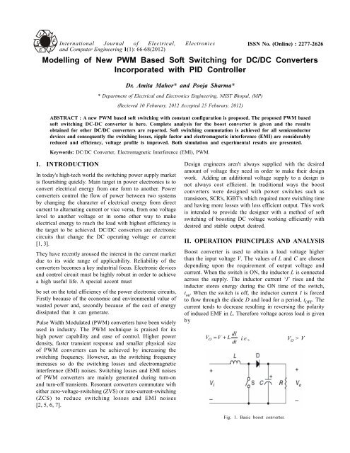
International Journal <strong>of</strong> Electrical, Electronics<br />
and Computer Engineering 1(1): 66-68(2012)<br />
<strong>Modelling</strong> <strong>of</strong> <strong>New</strong> <strong>PWM</strong> <strong>Based</strong> S<strong>of</strong>t <strong>Switching</strong> <strong>for</strong> <strong>DC</strong>/<strong>DC</strong> <strong>Converters</strong><br />
Incorporated with PID Controller<br />
Dr. Amita Mahor* and Pooja Sharma*<br />
* Department <strong>of</strong> Electrical and Electronics Engineering, NIIST Bhopal, (MP)<br />
(Recieved 10 Feburary, 2012 Accepted 25 Feburary, 2012)<br />
ABSTRACT : A new <strong>PWM</strong> based s<strong>of</strong>t switching with constant configuration is proposed. The proposed <strong>PWM</strong> based<br />
s<strong>of</strong>t switching <strong>DC</strong>-<strong>DC</strong> converter is here. Complete analysis <strong>for</strong> the boost converter is given and the results<br />
obtained <strong>for</strong> other <strong>DC</strong>/<strong>DC</strong> converters are reported. S<strong>of</strong>t switching commutation is achieved <strong>for</strong> all semiconductor<br />
devices and consequently the switching losses, ripple factor and electromagnetic interference (EMI) are considerably<br />
reduced and efficiency, voltage pr<strong>of</strong>ile is improved. Both simulation and experimental results are presented.<br />
Keywords: <strong>DC</strong>/<strong>DC</strong> Converter, Electromagnetic Interference (EMI), <strong>PWM</strong>.<br />
ISSN No. (Online) : 2277-2626<br />
I. INTRODUCTION<br />
In today's high-tech world the switching power supply market<br />
is flourishing quickly. Main target in power electronics is to<br />
convert electrical energy from one <strong>for</strong>m to another. Power<br />
converters control the flow <strong>of</strong> power between two systems<br />
by changing the character <strong>of</strong> electrical energy from direct<br />
current to alternating current or vice versa, from one voltage<br />
level to another voltage or in some other way to make<br />
electrical energy to reach the load with highest efficiency is<br />
the target to be achieved. <strong>DC</strong>/<strong>DC</strong> converters are electronic<br />
circuits that change the <strong>DC</strong> operating voltage or current<br />
[1, 3].<br />
They have recently aroused the interest in the current market<br />
due to its wide range <strong>of</strong> applicability. Reliability <strong>of</strong> the<br />
converters becomes a key industrial focus. Electronic devices<br />
and control circuit must be highly robust in order to achieve<br />
a high useful life. A special accent must<br />
be set on the total efficiency <strong>of</strong> the power electronic circuits,<br />
Firstly because <strong>of</strong> the economic and environmental value <strong>of</strong><br />
wasted power and, secondly because <strong>of</strong> the cost <strong>of</strong> energy<br />
dissipated that it can generate.<br />
Pulse Width Modulated (<strong>PWM</strong>) converters have been widely<br />
used in industry. The <strong>PWM</strong> technique is praised <strong>for</strong> its<br />
high power capability and ease <strong>of</strong> control. Higher power<br />
density, faster transient response and smaller physical size<br />
<strong>of</strong> <strong>PWM</strong> converters can be achieved by increasing the<br />
switching frequency. However, as the switching frequency<br />
increases so do the switching losses and electromagnetic<br />
interference (EMI) noises. <strong>Switching</strong> losses and EMI noises<br />
<strong>of</strong> <strong>PWM</strong> converters are mainly generated during turn-on<br />
and turn-<strong>of</strong>f transients. Resonant converters commutate with<br />
either zero-voltage-switching (ZVS) or zero-current-switching<br />
(ZCS) to reduce switching losses and EMI noises<br />
[2, 5, 6, 7].<br />
Design engineers aren't always supplied with the desired<br />
amount <strong>of</strong> voltage they need in order to make their design<br />
work. Adding an additional voltage supply to a design is<br />
not always cost efficient. In traditional ways the boost<br />
converters were designed with power switches such as<br />
transistors, SCR's, IGBT's which required more switching time<br />
and having more losses with less efficient output. This work<br />
is intended to provide the designer with a method <strong>of</strong> s<strong>of</strong>t<br />
switching <strong>of</strong> boosting <strong>DC</strong> voltage working efficiently with<br />
desired and stable output desired.<br />
II. OPERATION PRINCIPLES AND ANALYSIS<br />
Boost converter is used to obtain a load voltage higher<br />
than the input voltage V. The values <strong>of</strong> L and C are chosen<br />
depending upon the requirement <strong>of</strong> output voltage and<br />
current. When the switch is ON, the inductor L is connected<br />
across the supply. The inductor current ‘I’ rises and the<br />
inductor stores energy during the ON time <strong>of</strong> the switch,<br />
t on<br />
. When the switch is <strong>of</strong>f, the inductor current I is <strong>for</strong>ced<br />
to flow through the diode D and load <strong>for</strong> a period, t OFF<br />
. The<br />
current tends to decrease resulting in reversing the polarity<br />
<strong>of</strong> induced EMF in L. There<strong>for</strong>e voltage across load is given<br />
by<br />
dI<br />
= + i.e., V O<br />
> V<br />
VO<br />
V L dt<br />
Fig. 1. Basic boost converter.
A large capacitor ‘C’ connected across the load will provide<br />
a continuous output voltage. Diode D prevents any current<br />
flow from capacitor to the source.<br />
The circuit that models the basic operation <strong>of</strong> the boost<br />
converter is shown in Fig 1. The input voltage in series<br />
with the inductor acts as a current source. The energy stored<br />
in the inductor builds up when the switch is closed. When<br />
the switch is opened, current continues to flow through the<br />
inductor to the load. Since the source and the discharging<br />
inductor are both providing energy with the switch open,<br />
the effect is to boost the voltage across the load. The load<br />
consists <strong>of</strong> a resistor in parallel with a filter capacitor. The<br />
capacitor voltage is larger than the input voltage. The<br />
capacitor is large to keep a constant output voltage and<br />
acts to reduce the ripple in the output voltage. There are<br />
several assumptions to be made to analyze the ideal circuit:<br />
1. When the switch on, the drop across it is zero and the<br />
current through it is zero.<br />
2. The diode has zero voltage drops in conducting state and<br />
zero current in reverse-bias mode.<br />
3. The time delay in switching on and <strong>of</strong>f the switch and the<br />
diode are negligible.<br />
4. The inductor and capacitor are lossless.<br />
5. The response in the circuit is periodic. The value <strong>of</strong> inductor<br />
current at the start and end <strong>of</strong> a switching cycle is the<br />
same. The net increase in inductor current over a cycle is<br />
zero.<br />
6. The switch is made ON and OFF at a fixed frequency and<br />
let the period corresponding to the switching frequency be<br />
T. Given that the duty cycle is D, the switch is on <strong>for</strong> a<br />
period equal to DT, and the switch is <strong>of</strong>f <strong>for</strong> a time interval<br />
equal to (1 – D)T.<br />
7. The inductor current is continuous and is greater than zero<br />
8. The capacitor is relatively large. The RC time constant is<br />
so large, that the changes in capacitor voltage when the<br />
switch is ON or OFF can be neglected <strong>for</strong> calculating the<br />
change in inductor current and the average output voltage.<br />
The average output voltage is assumed to remain steady.<br />
converter. The proposed configuration achieves zero-voltage<br />
switching <strong>for</strong> the main switch and zero- current switching<br />
with zero-voltage at turn-<strong>of</strong>f <strong>for</strong> the auxiliary switch.<br />
Furthermore, there is no reverse- recovery problem <strong>for</strong> the<br />
main diode since its current decreases linearly [4].<br />
To analyses the steady state operation <strong>of</strong> the proposed<br />
mixed converter, the following assumptions are made:<br />
1. The output capacitor Co is large enough to assume that the<br />
output voltage Vo is constant and ripple free.<br />
2. The main inductor Lm is large enough to be treated as a<br />
constant-current source ILM.<br />
3. Main inductor Lm is much greater than resonant inductor Lr.<br />
4. The semiconductor devices and the reactive elements are ideal.<br />
Fig. 3. Block model <strong>of</strong> <strong>PWM</strong> based s<strong>of</strong>t switching<br />
Boost converter.<br />
IV. THE SOFT SWITCHING OF <strong>DC</strong>/<strong>DC</strong><br />
CONVERTERS<br />
The concept <strong>of</strong> the proposed s<strong>of</strong>t switching <strong>for</strong> the boost<br />
converter can be extended to other <strong>DC</strong>/<strong>DC</strong> converters. The<br />
three remaining topologies (Buck, Buck-boost and Cuk) were<br />
analyzed. Fig. 4 shows the four basic <strong>DC</strong>/<strong>DC</strong> converters<br />
feedback with linear system. The results <strong>of</strong> this analysis are<br />
reported.<br />
9. The source voltage VS remains constant.<br />
III. THE SOFT SWITCHING BOOST<br />
CONVERTER<br />
Fig. 2. Circuit diagram <strong>of</strong> the s<strong>of</strong>t switching <strong>of</strong> boost converter.<br />
Fig. 2 shows the proposed Snubber topology <strong>for</strong> the boost
68 Mahor and Sharma<br />
V. DESIGN EXAMPLE<br />
To verify the operation principles <strong>of</strong> the proposed converter,<br />
the following design specification <strong>for</strong> the boost converter is<br />
given here:<br />
V in<br />
= 24 V, V out<br />
= 48 V, I out<br />
= 0.1 A, L = 80 mh, C = 1.68 mf,<br />
RL = 80 m-ohms, RC = 5 m-ohms, R load<br />
= 120 ohms and<br />
fs = 100 kHz, <strong>PWM</strong> = 100 e3, PID controller = 0, 100, 0.<br />
VI. SIMULATED AND EXPERIMENTAL<br />
RESULTS<br />
The results <strong>for</strong> this specific design example were obtained<br />
using the simulink and are presented in Figure 4. As can be<br />
seen, the simulated results are in close agreement with the<br />
theoretical ones. The experimental wave<strong>for</strong>ms <strong>of</strong> the designed<br />
converter are presented in Fig. 5. It is clearly seen that the<br />
experimental results are in close agreement with the simulated<br />
ones.<br />
Fig. 4. Four basic circuits <strong>of</strong> <strong>DC</strong>/<strong>DC</strong> converters with s<strong>of</strong>t<br />
switching.<br />
VII. CONCLUSION<br />
In this paper, s<strong>of</strong>t switching <strong>PWM</strong> based <strong>DC</strong>/<strong>DC</strong> converters<br />
was proposed. To reduce switching losses and EMI noises<br />
to improve efficiency and voltage pr<strong>of</strong>ile, s<strong>of</strong>t switching was<br />
applied to all semiconductors devices in the new converters.<br />
The theoretical results <strong>for</strong> the proposed converter were<br />
confirmed by both simulated and experimental results.<br />
REFERENCES<br />
[1] N. Mohan, T. Undeland and W. Robbins, "Power Electronics:<br />
<strong>Converters</strong>, Applications and Design," John Wiley and sons,<br />
(1995).<br />
[2] G. Hua, C.S. Leu, Y. Jiang, and F.C. Lee, "Novel Zero-<br />
Voltage Transition <strong>PWM</strong> <strong>Converters</strong>," IEEE Trans. Power<br />
Electronics, Vol. 9, No. 2, pp. 213-219(1994).<br />
[3] A. Elasser and D.A. Torrey, "S<strong>of</strong>t <strong>Switching</strong> Active Snubber<br />
<strong>for</strong> <strong>DC</strong>/<strong>DC</strong> <strong>Converters</strong>," IEEE Trans. Power Electronics, Vol.<br />
11, No. 5, pp. 710-722(1996).<br />
[4] Milan M. Jovanovie and Yungtaek Jang, "A Novel <strong>for</strong> High-<br />
Power Boost <strong>Converters</strong>," IEEE Trans. Power Electronics,<br />
Vol. 15, No. 2, pp 278-284(2000).<br />
[5] G. Hua, E.X. Yang, Y. Jiang, and F.C. Lee, "Novel Zero-<br />
Current Transition <strong>PWM</strong> <strong>Converters</strong>," IEEE Trans. Power<br />
Electronics, Vol. 9, No. 6, pp. 601-606, (1994).<br />
[6] C.J. Tseng and C.L. Chen, "Novel ZVT-<strong>PWM</strong> <strong>Converters</strong><br />
with Active Snubber," IEEE Trans. Power Electronics, Vol.<br />
13, No. 5, pp. 861-869(1998).<br />
[7] P. Das and G. Moschopoulos, "A Comparative Study <strong>of</strong> Zero-<br />
Current-Transition <strong>PWM</strong> <strong>Converters</strong>", IEEE Transactions<br />
on Industrial Electronics, Vol. 54, pp. 1319-1328, June 20.<br />
Fig. 5. Simulated wave<strong>for</strong>ms <strong>of</strong> designed boost converter.