Design of Floating Gate Power Supply of Half-Bridge Circuit Using ...
Design of Floating Gate Power Supply of Half-Bridge Circuit Using ...
Design of Floating Gate Power Supply of Half-Bridge Circuit Using ...

You also want an ePaper? Increase the reach of your titles
YUMPU automatically turns print PDFs into web optimized ePapers that Google loves.
<strong>Design</strong> <strong>of</strong> <strong>Floating</strong> <strong>Gate</strong> <strong>Power</strong> <strong>Supply</strong> <strong>of</strong> <strong>Half</strong>-<strong>Bridge</strong> <strong>Circuit</strong> <strong>Using</strong><br />
Snubber Charge<br />
Se-Kyo Chung, Jung-Gyu Lim, Hwi-Beom Shin *, and Hyun-Woo Lee **<br />
* Department <strong>of</strong> Electrical and Electronics Engineering<br />
Gyeongsang National University, Jinju, Gyeongnam 660-701, Korea<br />
** Department <strong>of</strong> Electrical Engineering<br />
Kyungnam University, Masan, Gyeongnam, Korea<br />
Abstract<br />
This paper deals with a bootstrapped power supply using a snubber energy recovery for a high-side gate driver <strong>of</strong> a<br />
half-bridge inverter. The proposed circuit utilizes the snubber capacitor in the low-side power switch for charge<br />
pumping to a bootstrap capacitor used for a high-side floating power supply. By employing the proposed circuit, a<br />
simple floating power supply for a half-bridge inverter can be implemented without any magnetic components.<br />
Moreover, the power dissipation in the RCD snubber can be reduced by the energy recovery from the snubber capacitor.<br />
The operation principle and design method <strong>of</strong> the proposed circuit are presented. The simulation and experimental<br />
results are also provided to show the validity <strong>of</strong> the proposed circuit.<br />
Keywords: <strong>Gate</strong> driver, bootstrap circuit, snubber, energy recovery, half-bridge circuit<br />
1 INTRODUCTION<br />
A half-bridge topology is used as a basic building<br />
block for power conversion circuits such as single- and<br />
three-phase full-bridge converters. However, two<br />
isolated power supplies are generally required to<br />
control the gates <strong>of</strong> both high- and low-side power<br />
semiconductor switches because the high-side switch<br />
has a floating ground. This is a problem <strong>of</strong> significance<br />
in miniaturizing power converter circuits. The bootstrap<br />
and charge pump techniques have been considered as<br />
possible solutions to overcome this problem [1]-[5].<br />
A RCD snubber has been used to relieve a switching<br />
stress <strong>of</strong> a power semiconductor device during a<br />
turn-<strong>of</strong>f transition. Its configuration is simple but the<br />
power dissipation in the snubber resistor degrades<br />
efficiency <strong>of</strong> the power converter. Non-dissipative<br />
snubber circuits using energy regeneration have been<br />
presented [6], [7]. However, these circuits need<br />
additional magnetic components, such as transformers,<br />
for energy regeneration from the snubber capacitor.<br />
This paper deals with a bootstrapped power supply<br />
using snubber energy recovery for the high-side gate<br />
driver <strong>of</strong> a half-bridge inverter. In the proposed circuit,<br />
the snubber capacitor in the low-side power<br />
semiconductor switch is utilized for charge pumping to<br />
a bootstrap capacitor as well as original snubbing action.<br />
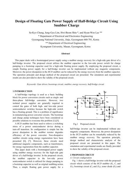
Thus, a simple floating gate power supply for a<br />
<br />
<br />
<br />
<br />
<br />
<br />
<br />
<br />
<br />
<br />
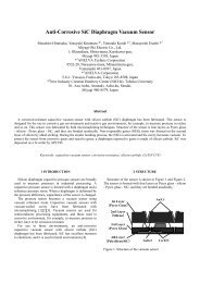
Fig.1 Proposed circuit.<br />
<br />
<br />
<br />
<br />
<br />
<br />
<br />
<br />
<br />
<br />
half-bridge inverter can be implemented without any<br />
magnetic components. Moreover, the power dissipation<br />
in the RCD snubber can be remarkably reduced by the<br />
snubber energy recovery. The operation principle,<br />
design method and characteristic analysis <strong>of</strong> the<br />
proposed circuit are presented in this paper. The<br />
simulation and experimental results are finally provided<br />
to show the validity <strong>of</strong> the proposed circuit.<br />
2 PROPOSED CIRCUIT<br />
A. <strong>Circuit</strong> configuration<br />
Fig. 1 shows a half-bridge inverter with the proposed<br />
circuit which consists <strong>of</strong> the RCD snubber (R s , C s and<br />
D s ), bootstrap circuit (C b and D b ), zener diode (D z ) and
initial charging circuit (D i and R i ). The MOSFETs are<br />
considered for the power semiconductor switches (S 1<br />
and S 2 ). The low-side gate driver is supplied from the<br />
independent DC source (V DC ) with a common ground.<br />
The details <strong>of</strong> the low-side circuit are omitted for<br />
simplicity.<br />
B. Operation <strong>of</strong> proposed circuit<br />
The operation <strong>of</strong> the proposed circuit can be<br />
explained using Fig. 2 which describes the operating<br />
modes <strong>of</strong> the proposed circuit. Each operating modes<br />
are explained as follows:<br />
• Initial charging: If the bootstrap and snubber<br />
capacitors are initially uncharged, it is required to<br />
charge one <strong>of</strong> two capacitors for starting up. As shown<br />
in Fig. 2(a), the low-side switch S 1 is first turned-on to<br />
charge C b using the power supply V DC , where the<br />
voltage across C b after initial charging is given as<br />
V = V −V<br />
−V<br />
. (1)<br />
cb, init DC Di S1(<br />
on)<br />
• Mode 1 (snubber capacitor charging): In this mode,<br />
after S 1 is turned-<strong>of</strong>f, S 2 is turned-on by using energy<br />
stored in C b as shown in Fig. 2(b). The capacitor C s is<br />
operated as a snubber during the turn-<strong>of</strong>f transition and<br />
charged by a surge and bus voltages. The stored charge<br />
in C s is given as<br />
Q = C v . (2)<br />
cs<br />
s<br />
cs<br />
As increasing the voltage across S 1 to V bus −V S2(on) , a<br />
bootstrap action occurs. The voltage potential at the top<br />
<strong>of</strong> C b (v cb + ) is highest in whole circuit. The current to<br />
maintain the on-state <strong>of</strong> S 2 should be supplied from C b<br />
during this mode.<br />
• Mode 2 (charge pumping): As shown in Fig. 2(c), S 2<br />
is turned-<strong>of</strong>f and S 1 is turned-on in this mode. The<br />
bootstrap capacitor C b is recharged by charge pumping<br />
from C s through D b . The voltage v cb is limited by a<br />
zener diode to V z . The charge stored in C b in this mode<br />
is given as<br />
Q = C V<br />
(3)<br />
cb<br />
b<br />
z<br />
• Mode 3 (snubber capacitor reset): The energy<br />
transfer from C s to C b is completed if the snubber<br />
capacitor voltage is down to v<br />
cs<br />
= Vz<br />
+ VDb<br />
+ VS1 ,( on)<br />
and<br />
the diode D b is turned <strong>of</strong>f. After that, the charge<br />
remained in C s is dissipated in R s for the next snubbing<br />
action.<br />
In the operation <strong>of</strong> the proposed circuit, the initial<br />
charging is needed once, only for starting up. Then, the<br />
Modes 1, 2 and 3 are repeated. After the initial charging,<br />
V DC is automatically disconnected from the proposed<br />
<br />
<br />
<br />
<br />
<br />
<br />
<br />
<br />
<br />
<br />
<br />
<br />
circuit if the zener breakdown voltage is chosen to be<br />
satisfied the condition given as<br />
V > V −V<br />
−V<br />
. (4)<br />
z<br />
<br />
<br />
<br />
<br />
<br />
<br />
<br />
<br />
<br />
<br />
<br />
<br />
<br />
<br />
<br />
<br />
<br />
<br />
<br />
DC<br />
Di<br />
<br />
<br />
<br />
<br />
<br />
<br />
<br />
<br />
<br />
S1(<br />
on)<br />
<br />
<br />
<br />
<br />
<br />
<br />
(a) Initial charging<br />
<br />
<br />
<br />
<br />
<br />
(b) Mode 1<br />
<br />
<br />
<br />
<br />
<br />
<br />
<br />
<br />
(c) Mode 2<br />
<br />
<br />
<br />
<br />
<br />
<br />
<br />
<br />
<br />
<br />
<br />
<br />
<br />
<br />
<br />
<br />
<br />
<br />
<br />
(d) Mode 3<br />
Fig. 2 Operation <strong>of</strong> proposed circuit.
3 DESIGN OF PROPOSED CIRCUIT<br />
A. Bootstrap and snubber capacitor values<br />
The values <strong>of</strong> the bootstrap and snubber capacitors<br />
can be calculated using the required charges and<br />
leakage currents <strong>of</strong> the high-side circuit. The amount <strong>of</strong><br />
the charge required in C b to drive S 2 during Mode 1 is<br />
represented as [1], [2]<br />
I + I + I + I<br />
qbs lgs lcb zk<br />
∆ Qcb<br />
= Qg<br />
+ Qls<br />
+<br />
. (5)<br />
f<br />
The minimum value <strong>of</strong> C b can be determined using (5)<br />
as<br />
∆Qcb<br />
Cb<br />
≥ . (6)<br />
∆v<br />
cb<br />
where ∆v cb is the desired ripple voltage in C b during<br />
Mode 1 defined by ∆ v = V −V<br />
. It is known from<br />
cb<br />
z<br />
cb , min<br />
(6) that choosing larger value <strong>of</strong> C b results in the lower<br />
ripple voltage. The minimum voltage V cb,min should be<br />
greater than a turn-<strong>of</strong>f threshold voltage <strong>of</strong> S 2 .<br />
Since the charge <strong>of</strong> C b is supplied from C s during<br />
Mode 2, the amount <strong>of</strong> the charge required in C s can<br />
represented as<br />
Ilcs<br />
∆ Qcs = ∆Qcb<br />
+ . (7)<br />
f<br />
The minimum value <strong>of</strong> C s can also be determined using<br />
(7) as<br />
∆Qcs<br />
Cs<br />
≥ (8)<br />
∆v<br />
where<br />
cs<br />
cs<br />
∆ v = V −V<br />
−V<br />
−V<br />
−V<br />
−V<br />
. (9)<br />
bus<br />
S 2(<br />
on)<br />
Ds Ds z S1(<br />
on)<br />
The value <strong>of</strong> Cs should meet the snubber requirement<br />
B. Diode ratings<br />
Under the above design, the charge supplied from C s<br />
to the high-side circuit is given as<br />
∆ Q ' = C ∆v<br />
≥ ∆Q<br />
. (10)<br />
cs<br />
s<br />
cs<br />
Since the charge consumed in the high-side circuit<br />
during Mode 1 is ∆ Q , the excess charge not stored in<br />
cb<br />
C b can be represented as<br />
∆ Q = ∆Q<br />
' −∆Q<br />
. (11)<br />
e<br />
cs<br />
cb<br />
This charge is dissipated in D z and S 1 . The average<br />
power loss by the dissipation <strong>of</strong> ∆Q<br />
in D z and S 1 can<br />
be calculated as<br />
P = ∆Q<br />
f ⋅V<br />
(12)<br />
z<br />
P<br />
e<br />
z<br />
cb<br />
e<br />
2<br />
( ∆Qe<br />
f ) ⋅ RDS1(<br />
)<br />
= ∆Q<br />
f ⋅V<br />
=<br />
. (13)<br />
S1 e S1(<br />
on)<br />
on<br />
The average currents <strong>of</strong> the bootstrap and snubber<br />
diodes D b and D s can be derived, respectively, as<br />
I = ∆Q<br />
' f<br />
(14)<br />
Db<br />
cs<br />
I = Q f . (15)<br />
Ds cs<br />
The peak current rating is important for the initial<br />
charging diode D i , which is calculated as<br />
I<br />
Di,<br />
peak<br />
V −V<br />
R + R<br />
DC Di<br />
= . (16)<br />
i<br />
Ds ( on)<br />
The peak inverse voltages <strong>of</strong> D b , D s and D i can also be<br />
derived, respectively, as<br />
V<br />
Db, PIV<br />
= Vz<br />
+ VDs<br />
(17)<br />
V = V −V<br />
−V<br />
. (18)<br />
Ds, PIV bus S 2( on)<br />
s1(<br />
on)<br />
Di, PIV<br />
= Vbus<br />
−VS<br />
2( on)<br />
+ Vz<br />
−VDC<br />
. (19)<br />
V<br />
C. Snubber resistor<br />
In Mode 3, the remained charge in C s is dissipated in<br />
R s and C s is then reset, where the reset time constant is<br />
given as τ = C R . The power loss in R s s can be<br />
calculated as<br />
s<br />
2<br />
( V + V + V ) ⋅ f<br />
1<br />
P = C<br />
(20)<br />
Rs<br />
s z Db S1(<br />
on)<br />
2<br />
It is noted that the power loss in R s is independent to the<br />
bus voltage.<br />
4 SIMULATIONS AND EXPERIMENTS<br />
A. Simulation and experimental conditions and device<br />
parameters<br />
The simulations and experiments were carried out to<br />
show the validity <strong>of</strong> the proposed circuit. Fig. 3 shows a<br />
test circuit used in both simulation and experiment. The<br />
MOSFET IXFH58N20 and fast recovery diode DSEI8<br />
by IXYS were used for the power switches (S 1 and S 2 )<br />
and diodes (D i , D b and D s ), respectively. The IR2110 by<br />
International Rectifiers was used as the gate drive for S 1<br />
and S 2 . The device parameters used in the simulation<br />
and experiment are summarized in Table 1.<br />
Fig. 3 Test circuit.<br />
<br />
<br />
<br />
<br />
<br />
<br />
<br />
<br />
<br />
<br />
<br />
<br />
<br />
<br />
<br />
<br />
<br />
<br />
<br />
<br />
<br />
The capacitor values can be calculated from (6) and<br />
(8) as C b ≥93.3nF and C s ≥9.7nF for ∆v cb =3V. The<br />
standard capacitor values with a margin were used in<br />
the simulation and experiment as C b =100nF and<br />
C s =22nF. Since metalized polyester capacitors with a<br />
small equivalent series resistance (ESR) were used for<br />
C b and C s , the leakage currents were neglected in this<br />
calculation. However, if electrolytic capacitors with a<br />
large ESR are used, the leakage currents should be<br />
considered. Since the power dissipation in R s is<br />
calculated as 0.03W, 10Ω/0.25W resistor was used.
Table 1 Experimental conditions and device parameters<br />
Item Value<br />
Experimental condition f 10kHz<br />
s V bus 50V<br />
MOSFET<br />
Zener diode<br />
Fast recovery diode<br />
<strong>Gate</strong> driver<br />
Q g<br />
I lgs<br />
R DS(on)<br />
V z<br />
I zk<br />
t rr<br />
225nC<br />
100nA<br />
40mΩ<br />
15V<br />
250uA<br />
35ns<br />
V Di , V Db , V Ds 1.0V<br />
I qbs<br />
Q ls<br />
230uA<br />
5nC<br />
V gs1<br />
0<br />
V gs2<br />
5V/div 0<br />
V cs<br />
10V/div<br />
0<br />
V cb<br />
2.5V/div<br />
0<br />
V ds2<br />
B. Simulation and experimental results<br />
The simulation was carried out using the Pspice. Fig.<br />
4 shows the simulation results for the test circuit as<br />
shown in Fig. 3. The gate-source voltages <strong>of</strong> S 1 and S 2 ,<br />
voltages across C s and C b , and drain-source voltage <strong>of</strong><br />
S 2 are shown from the top. It is shown in this figure that<br />
the high-side power switch is well controlled by using<br />
the proposed circuit.<br />
10V/div<br />
0<br />
50us/div <br />
Fig. 5 Experimental result for proposed circuit<br />
(Duty=50%)<br />
V gs1<br />
15V<br />
V gs2<br />
0<br />
V gs2<br />
0<br />
V gs1<br />
V gs2<br />
10V<br />
5V<br />
V gs1<br />
5V/div<br />
0V<br />
V cs<br />
60V<br />
10V/div<br />
V cs<br />
40V<br />
0<br />
20V<br />
0V<br />
V cb<br />
V cb<br />
15V<br />
10V<br />
5V<br />
2.5V/div<br />
0<br />
0V<br />
V ds2<br />
60V<br />
10V/div<br />
V ds2<br />
40V<br />
20V<br />
0V<br />
1.0ms 1.05ms 1.10ms 1.15ms 1.20ms 1.25ms 1.30ms<br />
0<br />
50us/div<br />
Fig. 6 Experimental result for proposed circuit<br />
(Duty=90%)<br />
Fig. 4 Simulation result.<br />
Figs. 5 through 7 show the experimental results for<br />
the test circuit. Fig. 6 shows the experimental results<br />
when a duty ratio <strong>of</strong> the high-side switching signal is<br />
given as 50%. It is shown in this figure that the<br />
proposed circuit well works as predicted in the<br />
simulation result. The voltage decrease in C b is<br />
dominant at the turn-on transition <strong>of</strong> S 2 . Thus, it can be<br />
known that the gate charge Q g is the most important
20V/div<br />
V cb<br />
0<br />
2.5V/div<br />
0<br />
V cb +<br />
V cs<br />
Fig. 7 Energy transfer from C s to C b .<br />
0.5us/div<br />
parameter in the design <strong>of</strong> the proposed circuit. It is<br />
impossible for bootstrapped power supplies to achieve a<br />
duty <strong>of</strong> 100% because the low-side switch must be<br />
turned-on to charge the bootstrap capacitor for one<br />
switching interval. Therefore, the operation under a<br />
high duty ratio is important for this type <strong>of</strong> the power<br />
supply. Fig. 6 shows the experimental results under a<br />
duty ratio <strong>of</strong> 90%. Fig. 7 shows the energy transfer<br />
from C s to C b during the turn-on transition <strong>of</strong> S 1 , where<br />
vcb+ means the voltage between the top <strong>of</strong> C b and<br />
common ground. It is shown in this figure that C b is<br />
charged during Mode 2 and C s is reset during Mode 3.<br />
5 CONCLUSIONS<br />
A floating gate power supply <strong>of</strong> a half-bridge circuit,<br />
using an energy recovery <strong>of</strong> a snubber capacitor, has<br />
been proposed. The proposed circuit can be simply<br />
implemented without any magnetic components.<br />
Moreover, the power dissipation in the RCD snubber<br />
can be reduced by the energy transfer to the high-side<br />
supply. It is, therefore, expected that the proposed<br />
circuit will be used for small-sized and low cost power<br />
conversion circuits using a half-bridge topology.<br />
ACKNOW LEDGEMENTS<br />
This work was financially supported by MOCIE<br />
through IERC program.<br />
V s2(on) =on-state voltage drop <strong>of</strong> S 2<br />
v cs =snubber capacitor voltage<br />
V bus =DC bus voltage<br />
V z =zener breakdown voltage<br />
V Db =forward voltage drop <strong>of</strong> the bootstrap diode<br />
V Ds =forward voltage drop <strong>of</strong> the snubber diode<br />
Q g =gate charge <strong>of</strong> S 2<br />
Q ls =level shifter charge <strong>of</strong> the gate driver<br />
I qbs =gate driver bias current<br />
I lgs =gate-source leakage current <strong>of</strong> S 2<br />
I lcb =leakage current <strong>of</strong> the bootstrap capacitor<br />
I zk =zener diode bias current<br />
I lcs =leakage current <strong>of</strong> the snubber capacitor<br />
REFERENCES<br />
[1] “HV floating MOS-gate driver ICs,” International<br />
Rectifier Application Note AN978-b, International<br />
Rectifier Co., El Segundo, CA, 2003.<br />
[2] J. Adams, “Bootstrap component selection for<br />
control IC’s,” International Rectifier <strong>Design</strong> Tip<br />
DT98-21, International Rectifier Co., El Segundo, CA,<br />
2001.<br />
[3] R. L. Lin and F. C. Lee, “Single power supply<br />
based transformerless IGBT/MOSFET gate driver with<br />
100% high-side turn-on duty cycle operation<br />
performance using auxiliary bootstrapped charge<br />
pumper,” in Conf. Rec. IEEE PESC ’97, pp. 1205-1209,<br />
1997.<br />
[4] G. F. W. Khoo, D. R. H. Carter, and R. A.<br />
McMahon, “Analysis <strong>of</strong> a charge pump power supply<br />
with a floating voltage reference,” IEEE Trans. <strong>Circuit</strong><br />
& Systems-I: Fund. Theory & Appl., vol. 47, no. 10, pp.<br />
1494-1501, 2000.<br />
[5] S. Park and T. M. Jahns, “A self-boost charge<br />
pump topology for a gated drive high-side power<br />
supply,” in Conf. Rec. IEEE APEC 2003, pp. 126-131,<br />
2003.<br />
[6] C. G. Steyn, “Analysis and optimization <strong>of</strong><br />
regenerative linear snubbers,” IEEE Trans. <strong>Power</strong><br />
Electron., vol. 4, no. 3, pp. 362-370, 1989.<br />
[7] J. F. Stephen, B. W. Williams, and T. C. Green,<br />
“RCD snubber revisited,” IEEE Trans. Ind. Appl., vol.<br />
32, no. 1, pp. 155-160, 1996.<br />
LIST OF SYMBOLS<br />
V DC = voltage <strong>of</strong> the low-side DC source<br />
V cb,init = initial charging voltage <strong>of</strong> the bootstrap<br />
capacitor<br />
V Di = forward voltage drop <strong>of</strong> the initial charging diode<br />
V s1(on) =on-state voltage drop <strong>of</strong> S 1