5804 BiMOS II UNIPOLAR STEPPER-MOTOR TRANSLATOR/DRIVER
5804 BiMOS II UNIPOLAR STEPPER-MOTOR TRANSLATOR/DRIVER
5804 BiMOS II UNIPOLAR STEPPER-MOTOR TRANSLATOR/DRIVER

You also want an ePaper? Increase the reach of your titles
YUMPU automatically turns print PDFs into web optimized ePapers that Google loves.
www.suc-tech.com<br />
<strong>5804</strong><br />
<strong>BiMOS</strong> <strong>II</strong> <strong>UNIPOLAR</strong><br />
<strong>STEPPER</strong>-<strong>MOTOR</strong><br />
<strong>TRANSLATOR</strong>/<strong>DRIVER</strong><br />
<strong>5804</strong><br />
<strong>BiMOS</strong> <strong>II</strong> <strong>UNIPOLAR</strong><br />
<strong>STEPPER</strong>-<strong>MOTOR</strong> <strong>TRANSLATOR</strong>/<strong>DRIVER</strong><br />
Data Sheet<br />
26184.12C<br />
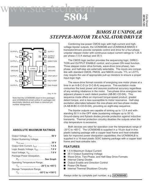
OUTPUT B<br />
K<br />
OUTPUT D<br />
GROUND<br />
GROUND<br />
OUTPUT C<br />
K<br />
BD<br />
AC<br />
OUTPUTA<br />
1<br />
2<br />
3<br />
4<br />
5<br />
6<br />
7<br />
8<br />
LOGIC<br />
V DD<br />
OE<br />
16<br />
15<br />
14<br />
13<br />
12<br />
11<br />
10<br />
9<br />
SUPPLY<br />
OUTPUT<br />
ENABLE<br />
DIRECTION<br />
GROUND<br />
GROUND<br />
STEP INPUT<br />
HALF-STEP<br />
ONE-PHASE<br />
Dwg. W-194<br />
Note that the UCN<strong>5804</strong>B (dual in-line package)<br />
and UCN<strong>5804</strong>LB (small outline IC package) are<br />
electrically identical and share a common pin<br />
number assignment.<br />
ABSOLUTE MAXIMUM RATINGS<br />
Output Voltage, V CE ...............................50 V<br />
Output Sustaining Voltage,<br />
V CE (sus) ............................................35 V<br />
Output Sink Current, I OUT .................... 1.5 A<br />
Logic Supply Voltage, V DD ....................7.0 V<br />
Input Voltage, V IN ..................................7.0 V<br />
Package Power Dissipation,<br />
P D ......................................... See Graph<br />
Operating Temperature Range,<br />
T A .................................. -20°C to +85°C<br />
Storage Temperature Range,<br />
T S ................................ -55°C to +150°C<br />
Combining low-power CMOS logic with high-current and highvoltage<br />
bipolar outputs, the UCN<strong>5804</strong>B and UCN<strong>5804</strong>LB <strong>BiMOS</strong> <strong>II</strong><br />
translator/drivers provide complete control and drive for a four-phase<br />
unipolar stepper-motor with continuous output current ratings to 1.25 A<br />
per phase (1.5 A startup) and 35 V.<br />
The CMOS logic section provides the sequencing logic, DIREC-<br />
TION and OUTPUT ENABLE control, and a power-ON reset function.<br />
Three stepper-motor drive formats, wave-drive (one-phase), twophase,<br />
and half-step are externally selectable. The inputs are compatible<br />
with standard CMOS, PMOS, and NMOS circuits. TTL or LSTTL<br />
may require the use of appropriate pull-up resistors to ensure a proper<br />
input-logic high.<br />
The wave-drive format consists of energizing one motor phase at a<br />
time in an A-B-C-D (or D-C-B-A) sequence. This excitation mode<br />
consumes the least power and assures positional accuracy regardless<br />
of any winding inbalance in the motor. Two-phase drive energizes two<br />
adjacent phases in each detent position (AB-BC-CD-DA). This<br />
sequence mode offers an improved torque-speed product, greater<br />
detent torque, and is less susceptible to motor resonance. Half-step<br />
excitation alternates between the one-phase and two-phase modes<br />
(A-AB-B-BC-C-CD-D-DA), providing an eight-step sequence.<br />
The bipolar outputs are capable of sinking up to 1.5 A and withstanding<br />
50 V in the OFF state (sustaining voltages up to 35 V).<br />
Ground-clamp and flyback diodes provide protection against inductive<br />
transients. Thermal protection circuitry disables the outputs when the<br />
chip temperature is excessive.<br />
Both devices are rated for operation over the temperature range of<br />
-20°C to +85°C. The UCN<strong>5804</strong>B is supplied in a 16-pin dual in-line<br />
plastic batwing package with a copper lead frame and heat-sinkable<br />
tabs for improved power dissipation capabilities; the UCN<strong>5804</strong>LB is<br />
supplied in a 16-lead plastic SOIC batwing package with a copper lead<br />
frame and heat-sinkable tabs.<br />
FEATURES<br />
■ 1.5 A Maximum Output Current<br />
■ 35 V Output Sustaining Voltage<br />
■ Wave-Drive, Two-Phase, and Half-Step Drive Formats<br />
■ Internal Clamp Diodes<br />
■ Output Enable and Direction Control<br />
■ Power-ON Reset<br />
■ Internal Thermal Shutdown Circuitry<br />
Always order by complete part number, e.g., UCN<strong>5804</strong>B .
www.suc-tech.com<br />
<strong>5804</strong><br />
<strong>BiMOS</strong> <strong>II</strong> <strong>UNIPOLAR</strong><br />
<strong>STEPPER</strong>-<strong>MOTOR</strong><br />
<strong>TRANSLATOR</strong>/<strong>DRIVER</strong><br />
TYPICAL INPUT CIRCUIT<br />
ALLOWABLE PACKAGE POWER DISSIPATION IN WATTS<br />
5<br />
R<br />
θJT<br />
= 6.0°C/W<br />
V DD<br />
4<br />
IN<br />
3<br />
SUFFIX 'B', R<br />
θJA<br />
= 43°C/W<br />
2<br />
Dwg. EP-010-5<br />
1<br />
SUFFIX 'LB', R<br />
θJA<br />
= 67°C/W<br />
TYPICAL OUTPUT <strong>DRIVER</strong><br />
0<br />
25 50 75 100 125 150<br />
TEMPERATURE IN °C<br />
K<br />
Dwg. GP-049-2<br />
OUT<br />
TRUTH TABLE<br />
Dwg. EP-021-4<br />
Drive Format Pin 9 Pin 10<br />
Two-Phase L L<br />
One-Phase H L<br />
Half-Step L H<br />
Step-Inhibit H H
www.suc-tech.com<br />
<strong>5804</strong><br />
<strong>BiMOS</strong> <strong>II</strong> <strong>UNIPOLAR</strong><br />
<strong>STEPPER</strong>-<strong>MOTOR</strong><br />
<strong>TRANSLATOR</strong>/<strong>DRIVER</strong><br />
ELECTRICAL CHARACTERISTICS at T A = 25°C, T J ≤ 150°C, V DD = 4.5 V to 5.5 V<br />
(unless otherwise noted).<br />
Limits<br />
Characteristic Symbol Test Conditions Min. Typ. Max. Units<br />
Output Leakage Current I CEX V OUT = 50 V — 10 50 µA<br />
Output Sustaining Voltage V CE(sus) I OUT = 1.25 A, L = 3 mH 35 — — V<br />
Output Saturation Voltage V CE(SAT) I OUT = 700 mA — 1.0 1.2 V<br />
I OUT = 1 A — 1.1 1.4 V<br />
I OUT = 1.25 A — 1.2 1.5 V<br />
Clamp Diode Leakage Current I R V R = 50 V — 10 50 µA<br />
Clamp Diode Forward Voltage V F I F = 1.25 A — 1.5 3.0 V<br />
Input Current I IN(1) V IN = V DD — 0.5 5.0 µA<br />
I IN(0) V IN = 0.8 V — -0.5 -5.0 µA<br />
Input Voltage V IN(1) V DD = 5 V 3.5 — 5.3 V<br />
V IN(0) -0.3 — 0.8 V<br />
Supply Current I DD 2 Outputs ON — 20 30 mA<br />
Turn-Off Delay t ON 50% Step Inputs to 50% Output — — 10 µs<br />
Turn-On Delay t OFF 50% Step Inputs to 50% Output — — 10 µs<br />
Thermal Shutdown Temperature T J — 165 — °C<br />
TIMING CONDITIONS<br />
CLOCK<br />
ONE PHASE<br />
C<br />
HALF STEP<br />
OOUTPUT ENABLE<br />
OUTPUT A<br />
OUTPUT B<br />
OUTPUT C<br />
A<br />
B<br />
OUTPUT D<br />
TWO -PHASE HALF-STEP WAVE DRIVE OUTPUT<br />
DISABLED<br />
Dwg. W-110A<br />
A. Minimum Data Set Up Time . . . . . . . . . . . . . . . . . . . . . . . . 100 ns<br />
B. Minimum Data Hold Time . . . . . . . . . . . . . . . . . . . . . . . . . . 100 ns<br />
C. Minimum Step Input Pulse Width . . . . . . . . . . . . . . . . . . . . . 3.0 µs
www.suc-tech.com<br />
<strong>5804</strong><br />
<strong>BiMOS</strong> <strong>II</strong> <strong>UNIPOLAR</strong><br />
<strong>STEPPER</strong>-<strong>MOTOR</strong><br />
<strong>TRANSLATOR</strong>/<strong>DRIVER</strong><br />
APPLICATIONS INFORMATION<br />
Internal power-ON reset (POR) circuitry<br />
resets OUTPUT A (and OUTPUT D in the twophase<br />
drive format) to the ON state with<br />
initial application of the logic supply voltage.<br />
After reset, the circuit then steps according to<br />
the tables.<br />
The outputs will advance one sequence<br />
position on the high-to-low transition of the<br />
STEP INPUT pulse. Logic levels on the<br />
HALF-STEP and ONE-PHASE inputs will<br />
determine the drive format (one-phase, twophase,<br />
or half-step). The DIRECTION pin<br />
determines the rotation sequence of the<br />
outputs. Note that the STEP INPUT must be<br />
in the low state when changing the state of<br />
ONE-PHASE, HALF-STEP, or DIRECTION<br />
to prevent erroneous stepping.<br />
All outputs are disabled (OFF) when<br />
OUTPUT ENABLE is at a logic high. If the<br />
function is not required, OUTPUT ENABLE<br />
should be tied low. In that condition, all<br />
outputs depend only on the state of the step<br />
logic.<br />
During normal commutation of a unipolar<br />
stepper motor, mutual coupling between the<br />
motor windings can force the outputs of the<br />
UCN<strong>5804</strong>B below ground. This condition will<br />
cause forward biasing of the collector-tosubstrate<br />
junction and source current from<br />
the output. For many L/R applications, this<br />
substrate current is high enough to adversely<br />
affect the logic circuitry and cause misstepping.<br />
External series diodes (Schottky are<br />
recommended for increased efficiency at lowvoltage<br />
operation) will prevent substrate<br />
current from being sourced through the<br />
outputs. Alternatively, external ground clamp<br />
diodes will provide a preferred current path<br />
from ground when the outputs are pulled<br />
below ground.<br />
WAVE-DRIVE SEQUENCE<br />
Half Step = L, One Phase = H<br />
Step A B C D<br />
POR ON OFF OFF OFF<br />
1 ON OFF OFF OFF<br />
2 OFF ON OFF OFF<br />
3 OFF OFF ON OFF<br />
4 OFF OFF OFF ON<br />
TWO-PHASE DRIVE SEQUENCE<br />
Half Step = L, One Phase = L<br />
Step A B C D<br />
POR ON OFF OFF ON<br />
1 ON OFF OFF ON<br />
2 ON ON OFF OFF<br />
3 OFF ON ON OFF<br />
4 OFF OFF ON ON<br />
HALF-STEP DRIVE SEQUENCE<br />
Half Step = H, One Phase = L<br />
Step A B C D<br />
POR ON OFF OFF OFF<br />
1 ON OFF OFF OFF<br />
2 ON ON OFF OFF<br />
3 OFF ON OFF OFF<br />
4 OFF ON ON OFF<br />
5 OFF OFF ON OFF<br />
6 OFF OFF ON ON<br />
7 OFF OFF OFF ON<br />
8 ON OFF OFF ON<br />
Internal thermal protection circuitry<br />
disables all outputs when the junction temperature<br />
reaches approximately 165°C. The<br />
outputs are enabled again when the junction<br />
cools down to approximately 145°C.
www.suc-tech.com<br />
<strong>5804</strong><br />
<strong>BiMOS</strong> <strong>II</strong> <strong>UNIPOLAR</strong><br />
<strong>STEPPER</strong>-<strong>MOTOR</strong><br />
<strong>TRANSLATOR</strong>/<strong>DRIVER</strong><br />
TYPICAL APPLICATION<br />
L/R Stepper-Motor Drive<br />
5V<br />
28V<br />
1<br />
V DD<br />
16<br />
2<br />
OE<br />
15<br />
3<br />
14<br />
DIRECTION<br />
CONTROL<br />
4<br />
5<br />
LOGIC<br />
13<br />
12<br />
6<br />
7<br />
8<br />
11<br />
10<br />
9<br />
STEP INPUT<br />
1<br />
V DD<br />
16<br />
2<br />
3<br />
OE<br />
15<br />
14<br />
OR<br />
4<br />
5<br />
LOGIC<br />
13<br />
12<br />
6<br />
11<br />
7<br />
10<br />
8<br />
9<br />
Dwg. EP-029A
www.suc-tech.com<br />
<strong>5804</strong><br />
<strong>BiMOS</strong> <strong>II</strong> <strong>UNIPOLAR</strong><br />
<strong>STEPPER</strong>-<strong>MOTOR</strong><br />
<strong>TRANSLATOR</strong>/<strong>DRIVER</strong><br />
UCN<strong>5804</strong>B<br />
Dimensions in Inches<br />
(controlling dimensions)<br />
16<br />
NOTE 4<br />
9<br />
0.020<br />
0.008<br />
0.280<br />
0.240<br />
0.430<br />
MAX<br />
0.300<br />
BSC<br />
1<br />
0.100<br />
8<br />
BSC<br />
0.070<br />
0.045<br />
0.775<br />
0.735<br />
0.005<br />
MIN<br />
0.210<br />
MAX<br />
0.015<br />
MIN<br />
0.150<br />
0.115<br />
0.022<br />
0.014<br />
Dwg. MA-001-17A in<br />
Dimensions in Millimeters<br />
(for reference only)<br />
16<br />
NOTE 4<br />
9<br />
0.508<br />
0.204<br />
7.11<br />
6.10<br />
7.62<br />
BSC<br />
10.92<br />
MAX<br />
1 8<br />
1.77<br />
1.15<br />
19.68<br />
18.67<br />
2.54<br />
BSC<br />
0.13<br />
MIN<br />
5.33<br />
MAX<br />
0.39<br />
MIN<br />
3.81<br />
2.93<br />
0.558<br />
0.356<br />
Dwg. MA-001-17A mm<br />
NOTES: 1. Exact body and lead configuration at vendor’s option within limits shown.<br />
2. Lead spacing tolerance is non-cumulative<br />
3. Lead thickness is measured at seating plane or below.<br />
4. Webbed lead frame. Leads 4, 5, 12, and 13 are internally one piece.
www.suc-tech.com<br />
<strong>5804</strong><br />
<strong>BiMOS</strong> <strong>II</strong> <strong>UNIPOLAR</strong><br />
<strong>STEPPER</strong>-<strong>MOTOR</strong><br />
<strong>TRANSLATOR</strong>/<strong>DRIVER</strong><br />
UCN<strong>5804</strong>LB<br />
Dimensions in Inches<br />
(for reference only)<br />
16 9<br />
0.0125<br />
0.0091<br />
0.2992<br />
0.2914<br />
0.419<br />
0.394<br />
0.050<br />
0.016<br />
0.020<br />
0.013<br />
1 2 3<br />
0.4133<br />
0.3977<br />
0.050<br />
BSC<br />
0° TO 8°<br />
0.0926<br />
0.1043<br />
0.0040 MIN.<br />
Dwg. MA-008-17A in<br />
16<br />
Dimensions in Millimeters<br />
(controlling dimensions)<br />
9<br />
0.32<br />
0.23<br />
7.60<br />
7.40<br />
10.65<br />
10.00<br />
1.27<br />
0.40<br />
0.51<br />
0.33<br />
1<br />
2 3<br />
10.50<br />
10.10<br />
1.27<br />
BSC<br />
0° TO 8°<br />
2.65<br />
2.35<br />
0.10 MIN.<br />
Dwg. MA-008-17A mm<br />
NOTES: 1. Exact body and lead configuration at vendor’s option within limits shown.<br />
2. Lead spacing tolerance is non-cumulative<br />
3. Lead thickness is measured at seating plane or below.<br />
4. Webbed lead frame. Leads 4, 5, 12, and 13 are internally one piece.
www.suc-tech.com<br />
<strong>5804</strong><br />
<strong>BiMOS</strong> <strong>II</strong> <strong>UNIPOLAR</strong><br />
<strong>STEPPER</strong>-<strong>MOTOR</strong><br />
<strong>TRANSLATOR</strong>/<strong>DRIVER</strong><br />
<strong>MOTOR</strong> <strong>DRIVER</strong>S SELECTION GUIDE<br />
Function Output Ratings * Part Number †<br />
INTEGRATED CIRCUITS FOR BRUSHLESS DC <strong>MOTOR</strong>S<br />
3-Phase Controller/Drivers ±2.0 A 45 V 2936 and 2936-120<br />
Hall-Effect Latched Sensors 10 mA 24 V 3175 and 3177<br />
2-Phase Hall-Effect Sensor/Controller 20 mA 25 V 3235<br />
Hall-Effect Complementary-Output Sensor 20 mA 25 V 3275<br />
2-Phase Hall-Effect Sensor/Driver 900 mA 14 V 3625<br />
2-Phase Hall-Effect Sensor/Driver 400 mA 26 V 3626<br />
Hall-Effect Complementary-Output Sensor/Driver 300 mA 60 V 5275<br />
3-Phase Back-EMF Controller/Driver ±900 mA 14 V 8902–A<br />
3-Phase Controller/DMOS Driver ±4.0 A 14 V 8925<br />
3-Phase Back-EMF Controller/Driver ±1.0 A 7 V 8984<br />
INTEGRATED BRIDGE <strong>DRIVER</strong>S FOR DC AND BIPOLAR <strong>STEPPER</strong> <strong>MOTOR</strong>S<br />
PWM Current-Controlled Dual Full Bridge ±750 mA 45 V 2916<br />
PWM Current-Controlled Dual Full Bridges ±1.5 A 45 V 2917 and 2918<br />
PWM Current-Controlled Dual Full Bridge ±750 mA 45 V 2919<br />
Dual Full-Bridge Driver ±2.0 A 50 V 2998<br />
PWM Current-Controlled Full Bridge ±2.0 A 50 V 3952<br />
PWM Current-Controlled Full Bridge ±1.3 A 50 V 3953<br />
PWM Current-Controlled Microstepping Full Bridges ±1.5 A 50 V 3955 and 3957<br />
PWM Current-Controlled Dual Full Bridge ±800 mA 33 V 3964<br />
PWM Current-Controlled Dual Full Bridge ±650 mA 30 V 3966 and 3968<br />
PWM Current-Controlled Dual Full Bridge ±750 mA 45 V 6219<br />
OTHER INTEGRATED CIRCUIT & PMCM <strong>MOTOR</strong> <strong>DRIVER</strong>S<br />
Unipolar Stepper-Motor Quad Driver 1.8 A 50 V 2544<br />
Unipolar Stepper-Motor Translator/Driver 1.25 A 50 V <strong>5804</strong><br />
Unipolar Stepper-Motor Quad Drivers 1 A 46 V 7024 and 7029<br />
Unipolar Microstepper-Motor Quad Driver 1.2 A 46 V 7042<br />
Voice-Coil Motor Driver ±500 mA 6 V 8932–A<br />
Voice-Coil Motor Driver ±800 mA 16 V 8958<br />
Voice-Coil (and Spindle) Motor Driver ±350 mA 7 V 8984<br />
* Current is maximum specified test condition, voltage is maximum rating. See specification for sustaining voltage<br />
limits or over-current protection voltage limits. Negative current is defined as coming out of (sourcing) the output.<br />
† Complete part number includes additional characters to indicate operating temperature range and package style.