Nios II Processor Reference Handbook
Nios II Processor Reference Handbook
Nios II Processor Reference Handbook

Create successful ePaper yourself
Turn your PDF publications into a flip-book with our unique Google optimized e-Paper software.
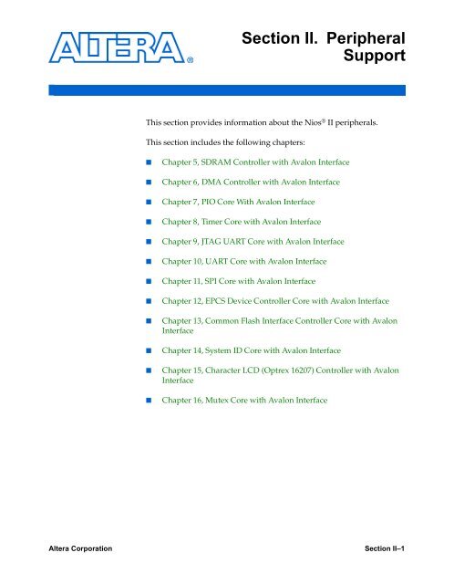
Section <strong>II</strong>. PeripheralSupportThis section provides information about the <strong>Nios</strong> ® <strong>II</strong> peripherals.This section includes the following chapters:■■■■■■■■■■■■Chapter 5, SDRAM Controller with Avalon InterfaceChapter 6, DMA Controller with Avalon InterfaceChapter 7, PIO Core With Avalon InterfaceChapter 8, Timer Core with Avalon InterfaceChapter 9, JTAG UART Core with Avalon InterfaceChapter 10, UART Core with Avalon InterfaceChapter 11, SPI Core with Avalon InterfaceChapter 12, EPCS Device Controller Core with Avalon InterfaceChapter 13, Common Flash Interface Controller Core with AvalonInterfaceChapter 14, System ID Core with Avalon InterfaceChapter 15, Character LCD (Optrex 16207) Controller with AvalonInterfaceChapter 16, Mutex Core with Avalon InterfaceAltera CorporationSection <strong>II</strong>–1
Peripheral Support<strong>Nios</strong> <strong>II</strong> <strong>Processor</strong> <strong>Reference</strong> <strong>Handbook</strong>Revision HistoryThe table below shows the revision history for Chapters 5 – 16. Theseversion numbers track the document revisions; they have no relationshipto the version of the <strong>Nios</strong> <strong>II</strong> development kits or <strong>Nios</strong> <strong>II</strong> processor coresChapter(s) Date / Version Changes Made5 September 2004, v1.1 Updates for <strong>Nios</strong> <strong>II</strong> 1.01 release.May 2004, v1.0First publication.6 December 2004, v1.2 ● Updated description of the GObit.● Updated descriptions ofioctl() macros in table 6-2.September 2004, v1.1May 2004, v1.0Updates for <strong>Nios</strong> <strong>II</strong> 1.01 release.First publication.7 September 2004, v1.1 Updates for <strong>Nios</strong> <strong>II</strong> 1.01 release.May 2004, v1.0First publication.8 September 2004, v1.1 Updates for <strong>Nios</strong> <strong>II</strong> 1.01 release.May 2004, v1.0First publication.9 December 2004, v1.2 Added Cyclone <strong>II</strong> support.September 2004, v1.1May 2004, v1.0Updates for <strong>Nios</strong> <strong>II</strong> 1.01 release.First publication.10 September 2004, v1.1 Updates for <strong>Nios</strong> <strong>II</strong> 1.01 release.May 2004, v1.0First publication.11 September 2004, v1.1 Updates for <strong>Nios</strong> <strong>II</strong> 1.01 release.May 2004, v1.0First publication.12 September 2004, v1.1 Updates for <strong>Nios</strong> <strong>II</strong> 1.01 release.May 2004, v1.0First publication.13 December 2004, v1.2 Added Cyclone <strong>II</strong> support.September 2004, v1.1May 2004, v1.0Updates for <strong>Nios</strong> <strong>II</strong> 1.01 release.First publication.14 September 2004, v1.1 Updates for <strong>Nios</strong> <strong>II</strong> 1.01 release.May 2004, v1.0First publication.Section <strong>II</strong>–2 Altera Corporation
Chapter(s) Date / Version Changes Made15 September 2004, v1.0 First publication.16 December 2004, v1.0 First publication.Altera Corporation 4–3<strong>Nios</strong> <strong>II</strong> <strong>Processor</strong> <strong>Reference</strong> <strong>Handbook</strong>
Peripheral Support4–4 Altera Corporation<strong>Nios</strong> <strong>II</strong> <strong>Processor</strong> <strong>Reference</strong> <strong>Handbook</strong>
5. SDRAM Controller withAvalon InterfaceN<strong>II</strong>51005-1.1Core OverviewThe SDRAM controller with Avalon interface provides an Avaloninterface to off-chip SDRAM. The SDRAM controller allows designers tocreate custom systems in an Altera ® FPGA that connect easily to SDRAMchips. The SDRAM controller supports standard SDRAM as described inthe PC100 specification.SDRAM is commonly used in cost-sensitive applications requiring largeamounts of volatile memory. While SDRAM is relatively inexpensive,control logic is required to perform refresh operations, open-rowmanagement, and other delays and command sequences. The SDRAMcontroller connects to one or more SDRAM chips, and handles allSDRAM protocol requirements. Internal to the FPGA, the core presentsan Avalon slave port that appears as linear memory (i.e., flat addressspace) to Avalon master peripherals.The core can access SDRAM subsystems with various data widths (8, 16,32, or 64 bits), various memory sizes, and multiple chip selects. TheAvalon interface is latency-aware, allowing read transfers to be pipelined.The core can optionally share its address and data buses with other offchipAvalon tristate devices. This feature is valuable in systems that havelimited I/O pins, yet must connect to multiple memory chips in additionto SDRAM.The SDRAM controller with Avalon Interface is SOPC Builder-ready andintegrates easily into any SOPC Builder-generated system.FunctionalDescriptionFigure 5–1 shows a block diagram of the SDRAM controller coreconnected to an external SDRAM chip.Altera Corporation 5–1September 2004
Functional DescriptionFigure 5–1. SDRAM Controller with Avalon Interface Block DiagramAltera FPGAPLLClock SkewAdjustmentSDRAM ControllerAvalon slaveinterfaceto on-chiplogicAvalonclockaddressdata, controlwaitrequestreaddatavalidAvalon Slave PortControlLogicInterface to SDRAM pinsckeaddrbacscasraswedqdqmclkPC 100SDRAMThe following sections describe the components of the SDRAM controllercore in detail. All options are specified at system generation time, andcannot be changed at run-time.Avalon InterfaceThe Avalon slave port is the only user-visible part of the SDRAMcontroller core. The slave port presents a flat, contiguous memory spaceas large as the SDRAM chip(s). When accessing the slave port, the detailsof the PC100 SDRAM protocol are entirely transparent. The Avaloninterface behaves as a simple memory interface. There are no memorymappedconfiguration registers.The Avalon slave port supports peripheral-controlled wait-states for readand write transfers. The slave port stalls the transfer until it can presentvalid data. The slave port also supports read transfers with variablelatency, enabling high-bandwidth, pipelined read transfers. When amaster peripheral reads sequential addresses from the slave port, the firstdata returns after an initial period of latency. Subsequent reads canproduce new data every clock cycle. However, data is not guaranteed toreturn every clock cycle, because the SDRAM controller must pauseperiodically to refresh the SDRAM.5–2 Altera Corporation<strong>Nios</strong> <strong>II</strong> <strong>Processor</strong> <strong>Reference</strong> <strong>Handbook</strong> September 2004
SDRAM Controller with Avalon InterfacefSee the Avalon Interface Specification <strong>Reference</strong> Manual for details onAvalon transfer types.Off-Chip SDRAM InterfaceThe interface to the external SDRAM chip presents the signals defined bythe PC100 standard. These signals must be connected externally to theSDRAM chip(s) via I/O pins on the Altera FPGA.Signal Timing & Electrical CharacteristicsThe timing and sequencing of signals depends on the configuration of thecore. The hardware designer configures the core to match the SDRAMchip chosen for the system. See “Instantiating the Core in SOPC Builder”on page 5–6 for details. The electrical characteristics of the FPGA pinsdepend on both the target device family and the assignments made in theQuartus ® <strong>II</strong> software. Some FPGA families support a wider range ofelectrical standards, and therefore are capable of interfacing with agreater variety of SDRAM chips. For details, see the handbook for thetarget FPGA family.SynchronizationThe SDRAM chip is driven at the same clock rate as the Avalon interface.As shown in Figure 5–1, an on-chip phase-locked loop (PLL) is often usedto alleviate clock skew between the SDRAM controller core and theSDRAM chip. At lower clock speeds, the PLL may not be necessary. Athigher clock rates, a PLL becomes necessary to tune the SDRAM clock totoggle within the window when signals are valid on the pins.The PLL block is not an integral part of the SDRAM controller core. If thePLL is necessary, the designer must manually instantiate the PLL outsidethe SOPC Builder-generated system module. Different combinations ofAltera FPGA and SDRAM chip will require different PLL settings.The SDRAM controller does not support clock-disable modes. TheSDRAM controller permanently asserts the cke pin.fThe <strong>Nios</strong> ® <strong>II</strong> development kit provides an example hardware design thatuses the SDRAM controller core in conjunction with a PLL.Sharing Pins with Other Avalon Tristate DevicesIf an Avalon tristate bridge is present in the SOPC Builder system, theSDRAM controller core can share pins with the existing tristate bridge. Inthis case, the core’s addr, dq (data) and dqm (byte-enable) pins are sharedwith other devices connected to the Avalon tristate bridge. This featureAltera Corporation 5–3September 2004<strong>Nios</strong> <strong>II</strong> <strong>Processor</strong> <strong>Reference</strong> <strong>Handbook</strong>
Functional Descriptionconserves I/O pins, which is valuable in systems that have multipleexternal memory chips (e.g., flash, SRAM, in addition to SDRAM), buttoo few pins to dedicate to the SDRAM chip. See “PerformanceConsiderations” on page 5–4 for details on how pin sharing affectsperformance.Performance ConsiderationsUnder optimal conditions, the SDRAM controller core’s bandwidthapproaches one word per clock cycle. However, because of the overheadassociated with refreshing the SDRAM, it is impossible to reach one wordper clock cycle. Other factors affect the core’s performance, as describedbelow.Open Row ManagementSDRAM chips are arranged as multiple banks of memory, wherein eachbank is capable of independent open-row address management. TheSDRAM controller core takes advantage of open-row management for asingle bank. Continuous reads or writes within the same row and bankwill operate at rates approaching one word per clock. Applications thatfrequently access different destination banks will require extramanagement cycles for row closings and openings.Sharing Data & Address PinsWhen the controller shares pins with other tristate devices, average accesstime usually increases while bandwidth decreases. When access to thetristate bridge is granted to other devices, the SDRAM requires row openand close overhead cycles. Furthermore, the SDRAM controller has towait several clock cycles before it is granted access again.To maximize bandwidth, the SDRAM controller automatically maintainscontrol of the tristate bridge as long as back-to-back read or writetransactions continue within the same row and bank.1 Note that this behavior may degrade the average access time forother devices sharing the Avalon tristate bridge.The SDRAM controller closes an open row whenever there is a break inback-to-back transactions, or whenever a refresh transaction is required.As a result:■■The controller cannot permanently block access to other devicessharing the tristate bridge.The controller is guaranteed not to violate the SDRAM’s row opentime limit.5–4 Altera Corporation<strong>Nios</strong> <strong>II</strong> <strong>Processor</strong> <strong>Reference</strong> <strong>Handbook</strong> September 2004
SDRAM Controller with Avalon InterfaceHardware Design & Target FPGAThe target FPGA affects the maximum achievable clock frequency of ahardware design. Certain device families achieve higher f MAXperformance than other families. Furthermore, within a device familyfaster speed grades achieve higher performance. The SDRAM controllercore can achieve 100 MHz in Altera’s high-performance device families,such as Stratix ® brand FPGAs. However, the core does not guarantee100 MHz performance in all Altera FPGA families.The f MAX performance also depends on the overall hardware design. Themaster clock for the SOPC Builder system module drives both theSDRAM controller core and the SDRAM chip. Therefore, the overallsystem module’s performance determines the performance of theSDRAM controller. For example, to achieve f MAX performance of100 MHz, the system module must be designed for a 100-MHz clock rate,and timing analysis in the Quartus <strong>II</strong> software must verify that thehardware design is capable of 100-MHz operation.Device & ToolsSupportThe SDRAM Controller with Avalon Interface core supports all AlteraFPGA families. Different FPGA families support different I/O standards,which may affect the ability of the core to interface to certain SDRAMchips. For details on supported I/O types, see the handbook for the targetFPGA family.Altera Corporation 5–5September 2004<strong>Nios</strong> <strong>II</strong> <strong>Processor</strong> <strong>Reference</strong> <strong>Handbook</strong>
Instantiating the Core in SOPC BuilderInstantiating theCore in SOPCBuilderDesigners use the configuration wizard for the SDRAM controller inSOPC Builder to specify hardware features and simulation features. TheSDRAM controller configuration wizard has two tabs: Memory Profileand Timing. This section describes the options available on each tab.The Presets list offers several pre-defined SDRAM configurations as aconvenience. If the SDRAM subsystem on the target board matches oneof the preset configurations, then the SDRAM controller core can beconfigured easily by selecting the appropriate preset value. The followingpreset configurations are defined:■ Micron MT8LSDT1664HG module■ Four SDR100 8 MByte x 16 chips■ Single Micron MT48LC2M32B2-7 chip■ Single Micron MT48LC4M32B2-7 chip■ Single NEC D4564163-A80 chip (64 MByte x 16)■ Single Alliance AS4LC1M16S1-10 chip■ Single Alliance AS4LC2M8S0-10 chipSelecting a preset configuration automatically changes values on theMemory Profile and Timing tabs to match the specific configuration.Altering a configuration setting on any tab changes the Preset value tocustom.5–6 Altera Corporation<strong>Nios</strong> <strong>II</strong> <strong>Processor</strong> <strong>Reference</strong> <strong>Handbook</strong> September 2004
SDRAM Controller with Avalon InterfaceMemory Profile TabThe Memory Profile tab allows designers to specify the structure of theSDRAM subsystem, such as address and data bus widths, the number ofchip select signals, and the number of banks. Table 5–1 lists the settingsavailable on the Memory Profile tab.Table 5–1. Memory Profile Tab SettingsSettingsAllowedValuesData Width 8, 16, 32,64ArchitectureSettingsAddressWidthSettingsDefaultValuesDescription32 SDRAM data bus width. This value determines the width ofthe dq bus (data) and the dqm bus (byte-enable).Chip Selects 1, 2, 4, 8 1 Number of independent chip selects in the SDRAMsubsystem. By using multiple chip selects, the SDRAMcontroller can combine multiple SDRAM chips into onememory subsystem.Banks 2, 4 4 Number of SDRAM banks. This value determines the widthof the ba bus (bank address) that connects to the SDRAM.The correct value is provided in the data sheet for the targetSDRAM.Row 11, 12,13, 14Column>= 8, andless thanRowvalue12 Number of row address bits. This value determines thewidth of the addr bus. The Row and Column valuesdepend on the geometry of the chosen SDRAM. Forexample, an SDRAM organized as 4096 (2 12 ) rows by 512columns has a Row value of 12.8 Number of column address bits. For example, the SDRAMorganized as 4096 rows by 512 (2 9 ) columns has a Columnvalue of 9.Controller sharesdq/dqm/addr I/O pinsInclude a functional memorymodel in the systemtestbenchYes, No No When set to No, all pins are dedicated to the SDRAM chip.When set to Yes, the addr, dq, and dqm pins can beshared with a tristate bridge in the system. In this case,SOPC Builder presents a new configuration tab that allowsthe user to associate the SDRAM controller pins with aspecific tristate bridge.Yes, No Yes When this option is turned on, SOPC Builder creates afunctional simulation model for the SDRAM chip. Thisdefault memory model accelerates the process of creatingand verifying systems that use the SDRAM controller. See“Hardware Simulation Considerations” on page 5–9.Altera Corporation 5–7September 2004<strong>Nios</strong> <strong>II</strong> <strong>Processor</strong> <strong>Reference</strong> <strong>Handbook</strong>
Instantiating the Core in SOPC BuilderBased on the settings entered on the Memory Profile tab, the wizarddisplays the expected memory capacity of the SDRAM subsystem in unitsof megabytes, megabits, and number of addressable words. It is useful tocompare these expected values to the actual size of the chosen SDRAM toverify that the settings are correct.Timing TabThe Timing tab allows designers to enter the timing specifications of theSDRAM chip(s) used. The correct values are provided in themanufacturer’s data sheet for the target SDRAM. Table 5–2 lists thesettings available on the Timing tab.Table 5–2. Timing Tab SettingsSettingsAllowedValuesDefaultValuesDescriptionCAS latency 1, 2, 3 3 Latency (in clock cycles) from a read command to data out.Initialization refreshcyclesIssue one refreshcommand everyDelay after power up,before initializationDuration of refreshcommand (t_rfc)Duration of prechargecommand (t_rp)ACTIVE to READ orWRITE delay (t_rcd)1 - 8 2 This value specifies how many refresh cycles the SDRAMcontroller will perform as part of the initialization sequence afterreset.– 15.625µsThis value specifies how often the SDRAM controller refreshesthe SDRAM. A typical SDRAM requires 4,096 refreshcommands every 64 ms, which can be met by issuing onerefresh command every 64 ms / 4,096 = 15.625 µs.– 100 µs The delay from stable clock and power to SDRAM initialization.– 70 ns Auto Refresh period.– 20 ns Precharge command period.– 20 ns ACTIVE to READ or WRITE delay.Access time (t_ac) – 17 ns Access time from clock edge. This value may depend on CASlatency.Write recovery time(t_wr, No autoprecharge)– 14 ns Write recovery if explicit precharge commands are issued. ThisSDRAM controller always issues explicit precharge commands.Regardless of the exact timing values input by the user, the actual timingachieved for each parameter will be integer multiples of the Avalon clock.For the Issue one refresh command every parameter, the actual timingwill be the greatest number of clock cycles that does not exceed the target5–8 Altera Corporation<strong>Nios</strong> <strong>II</strong> <strong>Processor</strong> <strong>Reference</strong> <strong>Handbook</strong> September 2004
SDRAM Controller with Avalon Interfacevalue. For all other parameters, the actual timing is the smallest numberof clock ticks that provides a value greater than or equal to the targetvalue.HardwareSimulationConsiderationsThis section discusses considerations for simulating systems withSDRAM. There are three major components required for simulation:■■■The simulation model for the SDRAM controllerThe simulation model for the SDRAM chip(s), also called thememory modelA simulation testbench that wires the memory model to the SDRAMcontroller pins.Some or all of these components are generated by SOPC Builder at systemgeneration time.SDRAM Controller Simulation ModelThe SDRAM controller design files generated by SOPC Builder aresuitable for both synthesis and simulation. Some simulation features areimplemented in the HDL using “translate on/off” synthesis directivesthat make certain sections of HDL code invisible to the synthesis tool.The simulation features are implemented primarily for easy simulation of<strong>Nios</strong> and <strong>Nios</strong> <strong>II</strong> processor systems using the ModelSim simulator. Thereis nothing ModelSim-specific about the SDRAM controller simulationmodel. However, minor changes may be required to make the modelwork with other simulators.cIf you change the simulation directives to create a customsimulation flow, be aware that SOPC Builder overwritesexisting files during system generation. Take precaution so thatyour changes are not overwritten.fRefer to AN 351: Simulating <strong>Nios</strong> <strong>II</strong> <strong>Processor</strong> Designs for a demonstrationof simulation of the SDRAM controller in the context of <strong>Nios</strong> <strong>II</strong>embedded processor systems.Altera Corporation 5–9September 2004<strong>Nios</strong> <strong>II</strong> <strong>Processor</strong> <strong>Reference</strong> <strong>Handbook</strong>
Hardware Simulation ConsiderationsSDRAM Memory ModelThere are two options for simulating a memory model of the SDRAMchip(s), as described below.Using the Generic Memory ModelIf the Include a functional memory model the system testbench optionis enabled at system generation, then SOPC Builder generates an HDLsimulation model for the SDRAM memory. In the auto-generated systemtestbench, SOPC Builder automatically wires this memory model to theSDRAM controller pins.Using the automatic memory model and testbench accelerates the processof creating and verifying systems that use the SDRAM controller.However, the memory model is a generic functional model that does notreflect the true timing or functionality of real SDRAM chips. The genericmodel is always structured as a single, monolithic block of memory. Forexample, even for a system that combines two SDRAM chips, the genericmemory model is implemented as a single entity.Using the SDRAM Manufacturer’s Memory ModelIf the Include a functional memory model the system testbench optionis not enabled, the designer is responsible for obtaining a memory modelfrom the SDRAM manufacturer, and manually wiring the model to theSDRAM controller pins in the system test bench.5–10 Altera Corporation<strong>Nios</strong> <strong>II</strong> <strong>Processor</strong> <strong>Reference</strong> <strong>Handbook</strong> September 2004
SDRAM Controller with Avalon InterfaceExampleConfigurationsThe following examples show how to connect the SDRAM controlleroutputs to an SDRAM chip or chips. The bus labeled ctl is an aggregate ofthe remaining signals, such as cas_n, ras_n, cke and we_n.Figure 5–2 shows a single 128-Mbit SDRAM chip with 32-bit data.Address, data and control signals are wired directly from the controller tothe chip. The result is a 128-Mbit (16-Mbyte) memory space.Figure 5–2. Single 128-Mbit SDRAM Chip with 32-Bit DataAltera FPGAAvaloninterfacetoon-chiplogicSDRAMControlleraddrctlcs_ndata 32 128 Mbits16 Mbytes32 data width deviceAltera Corporation 5–11September 2004<strong>Nios</strong> <strong>II</strong> <strong>Processor</strong> <strong>Reference</strong> <strong>Handbook</strong>
Example ConfigurationsFigure 5–3 shows two 64-Mbit SDRAM chips, each with 16-bit data.Address and control signals wire in parallel to both chips. Note thatchipselect (cs_n) is shared by the chips. Each chip provides half of the 32-bit data bus. The result is a logical 128-Mbit (16-Mbyte) 32-bit datamemory.Figure 5–3. Two 64-MBit SDRAM Chips Each with 16-Bit DataAltera FPGASDRAMControlleraddrctlcs_n64 Mbits8 Mbytes16 data width device16Avaloninterfacetoon-chiplogic64 Mbits8 Mbytes16 data width device16data325–12 Altera Corporation<strong>Nios</strong> <strong>II</strong> <strong>Processor</strong> <strong>Reference</strong> <strong>Handbook</strong> September 2004
SDRAM Controller with Avalon InterfaceFigure 5–4 shows two 128-Mbit SDRAM chips, each with 32-bit data.Control, address and data signals wire in parallel to the two chips. Thechipselect bus (cs_n[1:0]) determines which chip is selected. The resultis a logical 256-Mbit 32-bit wide memory.Figure 5–4. Two 128-Mbit SDRAM Chips Each with 32-Bit DataAltera FPGASDRAMControlleraddrctlcs_n [0]128 Mbits16 Mbytes32 data width device32Avaloninterfacetoon-chiplogic128 Mbits16 Mbytes32 data width device32cs_n [1]data 32SoftwareProgrammingModelThe SDRAM controller behaves like simple memory when accessed viathe Avalon interface. There are no software-configurable settings, andthere are no memory-mapped registers. No software driver routines arerequired for a processor to access the SDRAM controller.Altera Corporation 5–13September 2004<strong>Nios</strong> <strong>II</strong> <strong>Processor</strong> <strong>Reference</strong> <strong>Handbook</strong>
Software Programming Model5–14 Altera Corporation<strong>Nios</strong> <strong>II</strong> <strong>Processor</strong> <strong>Reference</strong> <strong>Handbook</strong> September 2004
6. DMA Controller withAvalon InterfaceN<strong>II</strong>51006-1.2Core OverviewThe Direct Memory Access (DMA) controller with Avalon interface(“the DMA controller”) performs bulk data transfers, reading data from asource address range and writing the data to a different address range.An Avalon master peripheral, such as a CPU, can offload memorytransfer tasks to the DMA controller. While the DMA controller performsmemory transfers, the master is free to perform other tasks in parallel.The DMA controller transfers data as efficiently as possible, reading andwriting data at the maximum pace allowed by the source or destination.The DMA controller is capable of performing streaming Avalon transfers,enabling it to automatically transfer data to or from a slow streamingperipheral (e.g., a universal asynchronous receiver/transmitter [UART]),at the maximum pace allowed by the peripheral.The DMA controller is SOPC Builder-ready and integrates easily into anySOPC Builder-generated system. For the <strong>Nios</strong> ® <strong>II</strong> processor, devicedrivers are provided in the HAL system library. See “SoftwareProgramming Model” on page 6–5 for details of HAL support.FunctionalDescriptionThe DMA controller is used to perform direct memory-access datatransfers from a source address-space to a destination address-space. Thesource and destination may be either an Avalon slave peripheral (i.e., aconstant address) or an address range in memory. The DMA controllercan be used in conjunction with streaming-capable peripherals, whichallows data transactions of fixed or variable length. The DMA controllercan signal an interrupt request (IRQ) when a DMA transaction completes.This document defines a transaction as a sequence of one or more Avalontransfers initiated by the DMA controller core.The DMA controller has two Avalon master ports—a master read portand a master write port—and one Avalon slave port for controlling theDMA as shown in Figure 6–1.Altera Corporation 6–1December 2004
Functional DescriptionFigure 6–1. X. DMA Controller Block DiagramAvalonslaveportAddr,data,controlIRQControlPortRegister FilestatusreadaddresswriteaddresslengthcontrolReadmasterportWritemasterportSeperateavalonmasterportsA typical DMA transaction proceeds as follows:1. A CPU prepares the DMA controller for a transaction by writing tothe control port.2. The CPU enables the DMA controller. The DMA controller thenbegins transferring data without additional intervention from theCPU. The DMA’s master read port reads data from the read address,which may be a memory or a peripheral. The master write portwrites the data to the destination address, which can also be amemory or peripheral. A shallow FIFO buffers data between theread and write ports.3. The DMA transaction ends when a specified number of bytes aretransferred (i.e., a fixed-length transaction), or an end-of-packetsignal is asserted by either the sender or receiver (i.e., a variablelengthtransaction). At the end of the transaction, the DMAcontroller generates an interrupt request (IRQ) if it was configuredby the CPU to do so.4. During or after the transaction, the CPU can determine if atransaction is in progress, or if the transaction ended (and how) byexamining the DMA controller’s status register.Setting Up DMA TransactionsAn Avalon master peripheral sets up and initiates DMA transactions bywriting to registers via the control port. The master peripheral configuresthe following options:■■Read (source) address locationWrite (destination) address location6–2 Altera Corporation<strong>Nios</strong> <strong>II</strong> <strong>Processor</strong> <strong>Reference</strong> <strong>Handbook</strong> December 2004
DMA Controller with Avalon Interface■■■■Size of the individual transfers: Byte (8-bit), halfword (16-bit), word(32-bit), doubleword (64-bit) or quadword (128-bit)Enable interrupt upon end of transactionEnable source or destination to end the DMA transaction with endof-packetsignalSpecify whether source and destination are memory or peripheralThe master peripheral then sets a bit in the control register to initiatethe DMA transaction.The Master Read & Write PortsThe DMA controller reads data from the source address through themaster read port, and then writes to the destination address through themaster write port. There is a shallow FIFO buffer between the master readand write ports. The default depth is 2, which makes the write actiondepend on the data-available status of the FIFO, rather than on the statusof the master read port.Both the read and write master ports are capable of performing Avalonstreaming transfers, which allows the slave peripheral to control the flowof data and terminate the DMA transaction.fFor details on streaming Avalon data transfers and streaming Avalonperipherals, see the Avalon Interface Specification <strong>Reference</strong> Manual.Address IncrementingWhen accessing memory, the read (or write) address increments by 1, 2,4, 8 or 16 after each access, depending on the width of the data. On theother hand, a typical peripheral device (such as UART) has fixed registerlocations. In this case, the read/write address is held constant throughoutthe DMA transaction.Altera Corporation 6–3December 2004<strong>Nios</strong> <strong>II</strong> <strong>Processor</strong> <strong>Reference</strong> <strong>Handbook</strong>
Instantiating the Core in SOPC BuilderThe rules for address incrementing are, in order of priority:■■If the control register’s RCON (or WCON) bit is set, the read (or write)increment value is 0.Otherwise, the read and write increment values are set according tothe transfer size specified in the control register, as shown inTable 6–1.Table 6–1. Address Increment ValuesTransfer WidthIncrementbyte 1halfword 2word 4doubleword 8quadword 16Instantiating theCore in SOPCBuilderDesigners use the DMA controller’s SOPC Builder configuration wizardto specify hardware options for the target system. Instantiating the DMAcontroller in SOPC Builder creates one slave port and two master ports.The designer must specify which slave peripherals can be accessed by theread and write master ports. Likewise, the designer must specify whichother master peripheral(s) can access the DMA control port and initiateDMA transactions. The DMA controller does not export any signals to thetop level of the system module.The configurable hardware features are described below.DMA Parameters (Basic)The following sections describe the basic parameters.Width of the DMA Length RegisterThis option sets the minimum width of the DMA’s transaction lengthregister. The acceptable range is 1 to 32. The length register determinesthe maximum number of transfers possible in a single DMA transaction.By default, the length register is wide enough to span any of the slaveperipherals mastered by the read or write ports. Overriding the lengthregister may be necessary if the DMA master port (read or write) mastersonly data peripherals, such as a UART. In this case, the address span ofeach slave is small, but a larger number of transfers may be desired perDMA transaction.6–4 Altera Corporation<strong>Nios</strong> <strong>II</strong> <strong>Processor</strong> <strong>Reference</strong> <strong>Handbook</strong> December 2004
DMA Controller with Avalon InterfaceConstruct FIFO from Registers vs. Construct FIFO from Memory BlocksThis option controls the implementation of the FIFO buffer between themaster read and write ports. When Construct FIFO from Registers isselected (the default), the FIFO is implemented using one register perstorage bit. This has a strong impact on logic utilization when the DMAcontroller’s data width is large (see “Advanced Options” on page 6–5).When Construct FIFO from Memory Blocks is selected, the FIFO isimplemented using embedded memory blocks available in the FPGA.Advanced OptionsThis section describes the advanced options.Allowed TransactionsThe designer can choose the transfer data width(s) supported by theDMA controller hardware. The following data-width options can beenabled or disabled:■■■■■ByteHalfword (two bytes)Word (four bytes)Doubleword (eight bytes)Quadword (sixteen bytes)Disabling unnecessary transfer widths reduces the amount of on-chiplogic resources consumed by the DMA controller core. For example, if asystem has both 16-bit and 32-bit memories, but the DMA controller willonly transfer data to the 16-bit memory, then 32-bit transfers could bedisabled to conserve logic resources.SoftwareProgrammingModelThis section describes the programming model for the DMA controller,including the register map and software declarations to access thehardware. For <strong>Nios</strong> <strong>II</strong> processor users, Altera provides HAL systemlibrary drivers that enable you to access the DMA controller core usingthe HAL API for DMA devices.HAL System Library SupportThe Altera-provided driver implements a HAL DMA device driver thatintegrates into the HAL system library for <strong>Nios</strong> <strong>II</strong> systems. HAL usersshould access the DMA controller via the familiar HAL API, rather thanaccessing the registers directly.Altera Corporation 6–5December 2004<strong>Nios</strong> <strong>II</strong> <strong>Processor</strong> <strong>Reference</strong> <strong>Handbook</strong>
Software Programming ModelcIf your program uses the HAL device driver to access the DMAcontroller, accessing the device registers directly will interferewith the correct behavior of the driver.The HAL DMA driver provides both ends of the DMA process; the driverregisters itself as both a receive channel (alt_dma_rxchan) and a transmitchannel (alt_dma_txchan). The <strong>Nios</strong> <strong>II</strong> Software Developer’s <strong>Handbook</strong>provides complete details of the HAL system library and the usage ofDMA devices.ioctl() Operationsioctl() operation requests are defined for both the receive and transmitchannels, which allows you to control the hardware-dependent aspects ofthe DMA controller. Two ioctl() functions are defined for the receiverdriver and the transmitter driver: alt_dma_rxchan_ioctl() andalt_dma_txchan_ioctl(). Table 6–2 lists the available operations.These are valid for both the transmit and receive channels.Table 6–2. Operations for alt_dma_rxchan_ioctl() & alt_dma_txchan_ioctl()RequestALT_DMA_SET_MODE_8ALT_DMA_SET_MODE_16ALT_DMA_SET_MODE_32ALT_DMA_SET_MODE_64ALT_DMA_SET_MODE_128ALT_DMA_RX_ONLY_ON (1)ALT_DMA_RX_ONLY_OFF (1)ALT_DMA_TX_ONLY_ON (1)ALT_DMA_TX_ONLY_OFF (1)MeaningTransfers data in units of 8 bits. The value of “arg” is ignored.Transfers data in units of 16 bits. The value of “arg” is ignored.Transfers data in units of 32 bits. The value of “arg” is ignored.Transfers data in units of 64 bits. The value of “arg” is ignored.Transfers data in units of 128 bits. The value of “arg” is ignored.Sets a DMA receiver into streaming mode. In this case, data is readcontinuously from a single location. The “arg” parameter specifies theaddress to read from.Turns off streaming mode for a receive channel. The value of “arg” isignored.Sets a DMA transmitter into streaming mode. In this case, data is writtencontinuously to a single location. The “arg” parameter specifies the addressto write to.Turns off streaming mode for a transmit channel. The value of “arg” isignored.Note to Table 6–2:(1) These macro names changed in version 1.1 of the <strong>Nios</strong> <strong>II</strong> development kit. The old names(ALT_DMA_TX_STREAM_ON, ALT_DMA_TX_STREAM_OFF, ALT_DMA_RX_STREAM_ON, andALT_DMA_RX_STREAM_OFF) are still valid, but new designs should use the new names.6–6 Altera Corporation<strong>Nios</strong> <strong>II</strong> <strong>Processor</strong> <strong>Reference</strong> <strong>Handbook</strong> December 2004
DMA Controller with Avalon InterfaceLimitationsCurrently the Altera-provided drivers do not support 64-bit and 128-bitDMA transactions.This function is not thread safe. If you want to access the DMA controllerfrom more than one thread then you should use a semaphore or mutex toensure that only one thread is executing within this function at any time.Software FilesThe DMA controller is accompanied by the following software files.These files define the low-level interface to the hardware. Applicationdevelopers should not modify these files.■■altera_avalon_dma_regs.h—This file defines the core’s register map,providing symbolic constants to access the low-level hardware. Thesymbols in this file are used only by device driver functions.altera_avalon_dma.h, altera_avalon_dma.c—These files implementthe DMA controller’s device driver for the HAL system library.Register MapProgrammers using the HAL API never access the DMA controllerhardware directly via its registers. In general, the register map is onlyuseful to programmers writing a device driver.cThe Altera-provided HAL device driver accesses the deviceregisters directly. If you are writing a device driver, and theHAL driver is active for the same device, your driver willconflict and fail to operate.Table 6–3 shows the register map for the DMA controller. Device driverscontrol and communicate with the hardware through five memorymapped32-bit registers.Table 6–3. DMA Controller Register MapOff-setRegisterNameRead/Write31. . .11109 8 7 6 5 4 3 2 1 00 status (1) RW (2) LEN1 readaddr RWRead master start addressessWEOPREOPBUSYDONEAltera Corporation 6–7December 2004<strong>Nios</strong> <strong>II</strong> <strong>Processor</strong> <strong>Reference</strong> <strong>Handbook</strong>
Software Programming ModelTable 6–3. DMA Controller Register MapOff-setRegisterName2 writeaddressRead/WriteRW31. . .11Write master start address3 length RW DMA transaction length (in bytes)4 - Reserved (3)5 - Reserved (3)6 control RW (2) (4)(5)WCONRCONLEENWEEN7 - Reserved (3)109 8 7 6 5 4 3 2 1 0REENNotes:(1) Writing zero to the status register clears the LEN, WEOP, REOP, and DONE bits.(2) These bits are reserved. Read values are undefined. Write zero.(3) This register is reserved. Read values are undefined. The result of a write is undefined.(4) QUADWORD.(5) DOUBLEWORD.I_ENGOWORDHWBYTEstatus RegisterThe status register consists of individual bits that indicate conditionsinside the DMA controller. The status register can be read at any time.Reading the status register does not change its value.The status register bits are shown in Table 6–4.Table 6–4. status Register BitsBit Number Bit Name Read/Write/Clear Description0 DONE R/C A DMA transaction is completed. The DONE bit is set to 1 whenan end of packet condition is detected or the specifiedtransaction length is completed. Write zero to the status registerto clear the DONE bit.1 BUSY R The BUSY bit is 1 when a DMA transaction is in progress.2 REOP R The REOP bit is 1 when a transaction is completed due to anend-of-packet event on the read side.3 WEOP R The WEOP bit is 1 when a transaction is completed due to anend of packet event on the write side.4 LEN R The LEN bit is set to 1 when the length register decrements tozero.6–8 Altera Corporation<strong>Nios</strong> <strong>II</strong> <strong>Processor</strong> <strong>Reference</strong> <strong>Handbook</strong> December 2004
DMA Controller with Avalon Interfacereadaddress RegisterThe readaddress register specifies the first location to be read in a DMAtransaction. The readaddress register width is determined at systemgeneration time. It is wide enough to address the full range of all slaveports mastered by the read port.writeaddress RegisterThe writeaddress register specifies the first location to be written in aDMA transaction. The writeaddress register width is determined atsystem generation time. It is wide enough to address the full range of allslave ports mastered by the write port.length RegisterThe length register specifies the number of bytes to be transferred fromthe read port to the write port. The length register is specified in bytes.For example, the value must be a multiple of 4 for word transfers, and amultiple of 2 for halfword transfers.The length register is decremented as each data value is written by thewrite master port. When length reaches 0 the LEN bit is set. The lengthregister does not decrement below 0.The length register width is determined at system generation time. It is atleast wide enough to span any of the slave ports mastered by the read orwrite master ports, and it can be made wider if necessary.control RegisterThe control register is composed of individual bits that control the DMA’sinternal operation. The control register’s value can be read at any time.The control register bits determine which, if any, conditions of the DMAtransaction result in the end of a transaction and an interrupt request.The control register bits are shown in Table 6–5.Table 6–5. control Register Bits (Part 1 of 2)Bit Number Bit Name Read/Write/Clear Description0 BYTE RW Specifies byte transfers.1 HW RW Specifies halfword (16-bit) transfers.2 WORD RW Specifies word (32-bit) transfers.Altera Corporation 6–9December 2004<strong>Nios</strong> <strong>II</strong> <strong>Processor</strong> <strong>Reference</strong> <strong>Handbook</strong>
Software Programming ModelTable 6–5. control Register Bits (Part 2 of 2)Bit Number Bit Name Read/Write/Clear Description3 GO RW Enables DMA transaction. When the GO bit is set to 0,the DMA is prevented from executing transfers. Whenthe GO bit is set to 1 and the length register is non-zero,transfers occur.4 I_EN RW Enables interrupt requests (IRQ). When the I_EN bit is 1,the DMA controller generates an IRQ when the statusregister’s DONE bit is set to 1. IRQs are disabled whenthe I_EN bit is 0.5 REEN RW Ends transaction on read-side end-of-packet. When theREEN bit is set to 1, a streaming slave port on the readside may end the DMA transaction by asserting its endof-packetsignal.6 WEEN RW Ends transaction on write-side end-of-packet. When theWEEN bit is set to 1, a streaming slave port on the writeside may end the DMA transaction by asserting its endof-packetsignal.7 LEEN RW Ends transaction when the length register reacheszero. When the LEEN bit is 1, the DMA transaction endswhen the length register reaches 0. When this bit is 0,length reaching 0 does not cause a transaction toend. In this case, the DMA transaction must beterminated by an end-of-packet signal from either theread or write master port.8 RCON RW Reads from a constant address. When RCON is 0, theread address increments after every data transfer. Thisis the mechanism for the DMA controller to read a rangeof memory addresses. When RCON is 1, the readaddress does not increment. This is the mechanism forthe DMA controller to read from a peripheral at aconstant memory address. For details, see “AddressIncrementing” on page 6–3.9 WCON RW Writes to a constant address. Similar to the RCON bit,when WCON is 0 the write address increments afterevery data transfer; when WCON is 1 the write addressdoes not increment. For details, see “AddressIncrementing” on page 6–3.10 DOUBLEWORD RW Specifies doubleword transfers.11 QUADWORD RW Specifies quadword transfers.The data width of DMA transactions is specified by the BYTE, HW,WORD, DOUBLEWORD, and QUADWORD bits. Only one of these bitscan be set at a time. If more than one of the bits is set, the DMA controllerbehavior is undefined. The width of the transfer is determined by the6–10 Altera Corporation<strong>Nios</strong> <strong>II</strong> <strong>Processor</strong> <strong>Reference</strong> <strong>Handbook</strong> December 2004
DMA Controller with Avalon Interfacenarrower of the two slaves read and written. For example, a DMAtransaction that reads from a 16-bit flash memory and writes to a 32-biton-chip memory requires a halfword transfer. In this case, HW must beset to 1, and BYTE, WORD, DOUBLEWORD, and QUADWORD must beset to 0.To successfully perform transactions of a specific width, that width mustbe enabled in hardware using the Allowed Transaction hardware option.For example, the DMA controller behavior is undefined if quadwordtransfers are disabled in hardware, but the QUADWORD bit is set duringa DMA transaction.Interrupt BehaviorThe DMA controller has a single IRQ output that is asserted when thestatus register’s DONE bit equals 1 and the control register’s I_EN bitequals 1.Writing the status register clears the DONE bit and acknowledges theIRQ. A master peripheral can read the status register and determinehow the DMA transaction finished by checking the LEN, REOP, andWEOP bits.Altera Corporation 6–11December 2004<strong>Nios</strong> <strong>II</strong> <strong>Processor</strong> <strong>Reference</strong> <strong>Handbook</strong>
Software Programming Model6–12 Altera Corporation<strong>Nios</strong> <strong>II</strong> <strong>Processor</strong> <strong>Reference</strong> <strong>Handbook</strong> December 2004
7. PIO Core With AvalonInterfaceN<strong>II</strong>51007-1.1Core OverviewThe parallel input/output (PIO) core provides a memory-mappedinterface between an Avalon slave port and general-purpose I/O ports.The I/O ports connect either to on-chip user logic, or to I/O pins thatconnect to devices external to the FPGA.The PIO core provides easy I/O access to user logic or external devices insituations where a “bit banging” approach is sufficient. Some exampleuses are:■■■■Controlling LEDsAcquiring data from switchesControlling display devicesConfiguring and communicating with off-chip devices, such asapplication-specific standard products (ASSP)The PIO core interrupt request (IRQ) output can assert an interrupt basedon input signals. The PIO core is SOPC Builder ready and integrateseasily into any SOPC Builder-generated system.FunctionalDescriptionEach PIO core can provide up to 32 I/O ports. An intelligent host such asa microprocessor controls the PIO ports by reading and writing theregister-mapped Avalon interface. Under control of the host, the PIO corecaptures data on its inputs and drives data to its outputs. When the PIOports are connected directly to I/O pins, the host can tristate the pins bywriting control registers in the PIO core. Figure 7–1 shows an example ofa processor-based system that uses multiple PIO cores to blink LEDs,capture edges from on-chip reset-request control logic, and control an offchipLCD display.Altera Corporation 7–1September 2004
Functional DescriptionFigure 7–1. An Example System Using Multiple PIO CoresAltera FPGACPUPIO core(output only)4LEDsAvalon Switch FabricIRQPIOcore Edge(input Captureonly)ResetrequestlogicProgramand DataMemoryPIOcore(bidirectional)11LCDdisplayWhen integrated into an SOPC Builder-generated system, the PIO corehas two user-visible features:■■A memory-mapped register space with four registers: data,direction, interruptmask, and edgecapture.1 to 32 I/O ports.The I/O ports can be connected to logic inside the FPGA, or to device pinsthat connect to off-chip devices. The registers provide an interface to theI/O ports via the Avalon interface. See Table 7–2 on page 7–7 for adescription of the registers. Some registers are not necessary in certainhardware configurations, in which case the unnecessary registers do notexist. Reading a non-existent register returns an undefined value, andwriting a non-existent register has no effect.Data Input & OutputThe PIO core I/O ports can connect to either on-chip or off-chip logic. Thecore can be configured with inputs only, outputs only, or both inputs andoutputs. If the core will be used to control bidirectional I/O pins on thedevice, the core provides a bidirectional mode with tristate control.7–2 Altera Corporation<strong>Nios</strong> <strong>II</strong> <strong>Processor</strong> <strong>Reference</strong> <strong>Handbook</strong> September 2004
PIO Core With Avalon InterfaceThe hardware logic is separate for reading and writing the data register.Reading the data register returns the value present on the input ports (ifpresent). Writing data affects the value driven to the output ports (ifpresent). These ports are independent; reading the data register does notreturn previously-written data.Edge CaptureThe PIO core can be configured to capture edges on its input ports. It cancapture low-to-high transitions, high-to-low transitions, or both.Whenever an input detects an edge, the condition is indicated in theedgecapture register. The type of edges to detect is specified at systemgeneration time, and cannot be changed via the registers.IRQ GenerationThe PIO core can be configured to generate an IRQ on certain inputconditions. The IRQ conditions can be either:■■Level-sensitive—The PIO core hardware can detect a high level. A NOTgate can be inserted external to the core to provide negativesensitivity.Edge-sensitive—The core’s edge capture configuration determineswhich type of edge causes an IRQInterrupts are individually maskable for each input port. The interruptmask determines which input port can generate interrupts.Altera Corporation 7–3September 2004<strong>Nios</strong> <strong>II</strong> <strong>Processor</strong> <strong>Reference</strong> <strong>Handbook</strong>
Example ConfigurationsExampleConfigurationsFigure 7–2 shows a block diagram of the PIO core configured with inputand output ports, as well as support for IRQs.Figure 7–2. PIO Core with Input & Output Ports & with IRQ SupportAvaloninterfaceto on-chiplogicaddressdatacontroldatainout3232interruptmaskIRQedgecaptureFigure 7–3 shows a block diagram of the PIO core configured inbidirectional mode, without support for IRQs.Figure 7–3. PIO Core with Bidirectional PortsAvaloninterfaceto on-chiplogicaddressdatacontroldatainout32directionAvalon InterfaceThe PIO core’s Avalon interface consists of a single Avalon slave port. Theslave port is capable of fundamental Avalon read and write transfers. TheAvalon slave port provides an IRQ output so that the core can assertinterrupts.Instantiating thePIO Core inSOPC BuilderThe hardware feature set is configured via the PIO core’s SOPC Builderconfiguration wizard. The following sections describe the availableoptions.7–4 Altera Corporation<strong>Nios</strong> <strong>II</strong> <strong>Processor</strong> <strong>Reference</strong> <strong>Handbook</strong> September 2004
PIO Core With Avalon InterfaceThe configuration wizard has two tabs, Basic Settings and InputOptions.Basic SettingsThe Basic Settings tab allows the designer to specify the width anddirection of the I/O ports.■The Width setting can be any integer value between 1 and 32. For avalue of n, the I/O ports become n-bits wide.■ The Direction setting has four options, as shown in Table 7–1.Table 7–1. Direction SettingsSettingBidirectional (tristate) portsInput ports onlyOutput ports onlyBoth input and output portsDescriptionIn this mode, each PIO bit shares one device pin for driving and capturing data.The direction of each pin is individually selectable. To tristate an FPGA I/O pin, setthe direction to input.In this mode the PIO ports can capture input only.In this mode the PIO ports can drive output only.In this mode, the input and output ports buses are separate, unidirectional busesof n bits wide.Input OptionsThe Input Options tab allows the designer to specify edge-capture andIRQ generation settings. The Input Options tab is not available whenOutput ports only is selected on the Basic Settings tab.Edge Capture RegisterWhen the Synchronously capture option is turned on, the PIO corecontains the edge capture register, edgecapture. The user must furtherspecify what type of edge(s) to detect:■■■Rising EdgeFalling EdgeEither EdgeThe edge capture register allows the core to detect and (optionally)generate an interrupt when an edge of the specified type occurs on aninput port.Altera Corporation 7–5September 2004<strong>Nios</strong> <strong>II</strong> <strong>Processor</strong> <strong>Reference</strong> <strong>Handbook</strong>
Device & Tools SupportWhen the Synchronously capture option is turned off, the edgecaptureregister does not exist.InterruptWhen the Generate IRQ option is turned on, the PIO core is able to assertan IRQ output when a specified event occurs on input ports. The usermust further specify the cause of an IRQ event:■■Level—The core generates an IRQ whenever a specific input is highand interrupts are enabled for that input in the interruptmaskregister.Edge—The core generates an IRQ whenever a specific bit in the edgecapture register is high and interrupts are enabled for that bit in theinterruptmask register.When the Generate IRQ option is turned off, the interruptmaskregister does not exist.Device & ToolsSupportSoftwareProgrammingModelfThe PIO core supports all Altera ® FPGA families.This section describes the software programming model for the PIO core,including the register map and software constructs used to access thehardware. For <strong>Nios</strong> ® <strong>II</strong> processor users, Altera provides the HAL systemlibrary header file that defines the PIO core registers. The PIO core doesnot match the generic device model categories supported by the HAL, soit cannot be accessed via the HAL API or the ANSI C standard library.The <strong>Nios</strong> <strong>II</strong> Development Kit provides several example designs thatdemonstrate usage of the PIO core. In particular, the count_binary.cexample uses the PIO core to drive LEDs, and detect button pressesusing PIO edge-detect interrupts.Software FilesThe PIO core is accompanied by one software file,altera_avalon_pio_regs.h. This file defines the core’s register map,providing symbolic constants to access the low-level hardware.7–6 Altera Corporation<strong>Nios</strong> <strong>II</strong> <strong>Processor</strong> <strong>Reference</strong> <strong>Handbook</strong> September 2004
PIO Core With Avalon InterfaceLegacy SDK RoutinesThe PIO core is supported by the legacy SDK routines for the firstgeneration<strong>Nios</strong> processor. For details on these routines, refer to the PIOdocumentation that accompanied the first-generation <strong>Nios</strong> processor. Fordetails on upgrading programs based on the legacy SDK to the HALsystem library API, refer to AN 350: Upgrading <strong>Nios</strong> <strong>Processor</strong> Systems to the<strong>Nios</strong> <strong>II</strong> <strong>Processor</strong>.Register MapAn Avalon master peripheral, such as a CPU, controls and communicateswith the PIO core via the four 32-bit registers, shown in Table 7–2. Thetable assumes that the PIO core’s I/O ports are configured to a width of nbits.Table 7–2. Register Map for the PIO CoreOffset Register Name R/W (n-1) ... 2 1 00 data read access R Data value currently on PIO inputswrite access W New value to drive on PIO outputs1 direction (1) R/W Individual direction control for each I/O port. A value of 0sets the direction to input; 1 sets the direction to output.2 interruptmask (1) R/W IRQ enable/disable for each input port. Setting a bit to 1enables interrupts for the corresponding port.3 edgecapture (1), (2) R/W Edge detection for each input port.Notes to Table 7–2:(1) This register may not exist, depending on the hardware configuration. If a register is not present, reading theregister returns an undefined value, and writing the register has no effect.(2) Writing any value to edgecapture clears all bits to 0.data RegisterReading from data returns the value present at the input ports. If the PIOcore hardware is configured in output-only mode, reading from datareturns an undefined value.Writing to data stores the value to a register that drives the output ports.If the PIO core hardware is configured in input-only mode, writing todata has no effect. If the PIO core hardware is in bidirectional mode, theregistered value appears on an output port only when the correspondingbit in the direction register is set to 1 (output).Altera Corporation 7–7September 2004<strong>Nios</strong> <strong>II</strong> <strong>Processor</strong> <strong>Reference</strong> <strong>Handbook</strong>
Software Programming Modeldirection RegisterThe direction register controls the data direction for each PIO port,assuming the port is bidirectional. When bit n in direction is set to 1,port n drives out the value in the corresponding bit of the data register.The direction register only exists when the PIO core hardware isconfigured in bidirectional mode. The mode (input, output, orbidirectional) is specified at system generation time, and cannot bechanged at runtime. In input-only or output-only mode, the directionregister does not exist. In this case, reading direction returns anundefined value, writing direction has no effect.After reset, all bits of direction are 0, so that all bidirectional I/O ports areconfigured as inputs. If those PIO ports are connected to device pins, thepins are held in a high-impedance state.interruptmask RegisterSetting a bit in the interruptmask register to 1 enables interrupts forthe corresponding PIO input port. Interrupt behavior depends on thehardware configuration of the PIO core. See “Interrupt Behavior” onpage 7–9.The interruptmask register only exists when the hardware isconfigured to generate IRQs. If the core cannot generate IRQs, readinginterruptmask returns an undefined value, and writing tointerruptmask has no effect.After reset, all bits of interruptmask are zero, so that interrupts aredisabled for all PIO ports.edgecapture RegisterBit n in the edgecapture register is set to 1 whenever an edge is detectedon input port n. An Avalon master peripheral can read the edgecaptureregister to determine if an edge has occurred on any of the PIO inputports. Writing any value to edgecapture clears all bits in the register.The type of edge(s) to detect is fixed in hardware at system generationtime. The edgecapture register only exists when the hardware isconfigured to capture edges. If the core is not configured to capture edges,reading from edgecapture returns an undefined value, and writing toedgecapture has no effect.7–8 Altera Corporation<strong>Nios</strong> <strong>II</strong> <strong>Processor</strong> <strong>Reference</strong> <strong>Handbook</strong> September 2004
PIO Core With Avalon InterfaceInterrupt BehaviorThe PIO core outputs a single interrupt-request (IRQ) signal that canconnect to any master peripheral in the system. The master can readeither the data register or the edgecapture register to determine whichinput port caused the interrupt.When the hardware is configured for level-sensitive interrupts, the IRQ isasserted whenever corresponding bits in the data and interruptmaskregisters are 1. When the hardware is configured for edge-sensitiveinterrupts, the IRQ is asserted whenever corresponding bits in theedgecapture and interruptmask registers are 1. The IRQ remainsasserted until explicitly acknowledged by disabling the appropriate bit(s)in interruptmask, or by writing to edgecapture.Software FilesThe PIO core is accompanied by the following software file. This fileprovide low-level access to the hardware. Application developers shouldnot modify the file.■altera_avalon_pio_regs.h—This file defines the core’s register map,providing symbolic constants to access the low-level hardware. Thesymbols in this file are used by device driver functions.Altera Corporation 7–9September 2004<strong>Nios</strong> <strong>II</strong> <strong>Processor</strong> <strong>Reference</strong> <strong>Handbook</strong>
Software Programming Model7–10 Altera Corporation<strong>Nios</strong> <strong>II</strong> <strong>Processor</strong> <strong>Reference</strong> <strong>Handbook</strong> September 2004
8. Timer Core with AvalonInterfaceN<strong>II</strong>51008-1.1Core OverviewThe timer core with Avalon interface core is a 32-bit interval timer forAvalon-based processor systems, such as a <strong>Nios</strong> ® <strong>II</strong> processor system. Thetimer provides the following features:■■■■■■■Controls to start, stop, and reset the timerTwo count modes: count down once and continuous count-downCount-down period registerMaskable interrupt request (IRQ) upon reaching zeroOptional watchdog timer feature that resets the system if timer everreaches zeroOptional periodic pulse generator feature that outputs a pulse whentimer reaches zeroCompatible with 32-bit and 16-bit processorsDevice drivers are provided in the HAL system library for the <strong>Nios</strong> <strong>II</strong>processor. The timer core is SOPC Builder-ready and integrates easily intoany SOPC Builder-generated system.FunctionalDescriptionFigure 8–1 shows a block diagram of the timer core.Figure 8–1. Timer Core Block DiagramRegister FilestatusAddress, data,etc.controlperiodlAvalonslaveinterfaceto on-chiplogicIRQresetrequest(watchdog)periodhsnaplsnaphControlLogicCountertimeout_pulseAltera Corporation 8–1September 2004
Functional DescriptionThe timer core has two user-visible features:■■The Avalon interface that provides access to six 16-bit registersAn optional pulse output that can be used as a periodic pulsegeneratorAll registers are 16-bits wide, making the timer compatible with both 16-bit and 32-bit processors. Certain registers only exist in hardware for agiven configuration. For example, if the timer is configured with a fixedperiod, the period registers do not exist in hardware.The basic behavior of the timer is described below:■■■■■■An Avalon master peripheral, such as a <strong>Nios</strong> <strong>II</strong> processor, writes thetimer core’s control register to:● Start and stop the timer● Enable/disable the IRQ● Specify count-down once or continuous count-down modeA processor reads the status register for information about currenttimer activity.A processor can specify the timer period by writing a value to theperiod registers, periodl and periodh.An internal counter counts down to zero, and whenever it reacheszero, it is immediately reloaded from the period registers.A processor can read the current counter value by first writing toeither snapl or snaph to request a coherent snapshot of the counter,and then reading snapl and snaph for the full 32-bit value.When the count reaches zero:● If IRQs are enabled, an IRQ is generated● The (optional) pulse-generator output is asserted for one clockperiod● The (optional) watchdog output resets the systemAvalon Slave InterfaceThe timer core implements a simple Avalon slave interface to provideaccess to the register file. The Avalon slave port uses the resetrequestsignal to implement watchdog timer behavior. This signal is a nonmaskablereset signal, and it drives the reset input of all Avalonperipherals in the SOPC Builder system. When the resetrequestsignal is asserted, it forces any processor connected to the system toreboot. See “Configuring the Timer as a Watchdog Timer” on page 8–4 forfurther details.8–2 Altera Corporation<strong>Nios</strong> <strong>II</strong> <strong>Processor</strong> <strong>Reference</strong> <strong>Handbook</strong> September 2004
Timer Core with Avalon InterfaceDevice & ToolsSupportInstantiating theCore in SOPCBuilderThe timer core supports all Altera ® FPGA families.Designers use the timer’s SOPC Builder configuration wizard to specifythe hardware features. This section describes the options available in theconfiguration wizard.Timeout PeriodThe Timeout Period setting determines the initial value of the periodland periodh registers. When the Writeable period setting is enabled, aprocessor can change the value of the period by writing periodl andperiodh. When the Writeable period setting (see below) is turned off,the period is fixed and cannot be updated at runtime.The Timeout Period setting can be specified in units of usec, msec, sec, orclocks (number of clock cycles). The actual period achieved depends onthe system clock. If the period is specified in usec, msec or sec, the trueperiod will be the smallest number of clock cycles that is greater than orequal to the specified Timeout Period.Hardware OptionsThe following options affect the hardware structure of the timer core. Asa convenience, the Preset Configurations list offers several pre-definedhardware configurations, such as:■■■Simple periodic interrupt—This configuration is useful for systemsthat require only a periodic IRQ generator. The period is fixed andthe timer cannot be stopped, but the IRQ can be disabled.Full-featured—This configuration is useful for embedded processorsystems that require a timer with variable period that can be startedand stopped under processor control.Watchdog—This configuration is useful for systems that requirewatchdog timer to reset the system in the event that the system hasstopped responding. See “Configuring the Timer as a WatchdogTimer” on page 8–4.Altera Corporation 8–3September 2004<strong>Nios</strong> <strong>II</strong> <strong>Processor</strong> <strong>Reference</strong> <strong>Handbook</strong>
Instantiating the Core in SOPC BuilderRegister OptionsTable 8–1 shows the settings that affect the timer core’s registers.Table 8–1. Register OptionsOptionWriteableperiodReadablesnapshotStart/Stopcontrol bitsDescriptionWhen this option is enabled, a master peripheral can change the count-down period by writingperiodl and periodh. When disabled, the count-down period is fixed at the specifiedTimeout Period, and the periodl and periodh registers do not exist in hardware.When this option is enabled, a master peripheral can read a snapshot of the current countdown.When disabled, the status of the counter is detectable only via other indicators, such asthe status register or the IRQ signal. In this case, the snapl and snaph registers do notexist in hardware, and reading these registers produces an undefined value.When this option is enabled, a master peripheral can start and stop the timer by writing theSTART and STOP bits in the control register. When disabled, the timer runs continuously.When the System reset on timeout (watchdog) option is enabled, the START bit is alsopresent, regardless of the Start/Stop control bits option.Output Signal OptionsTable 8–2 shows the settings that affect the timer core’s output signals.Table 8–2. Output Signal OptionsOptionTimeout pulse (1clock wide)System reset ontimeout (watchdog)DescriptionWhen this option is enabled, the timer core outputs a signal timeout_pulse. This signalpulses high for one clock cycle whenever the timer reaches zero. When disabled, thetimeout_pulse signal does not exist.When this option is enabled, the timer core’s Avalon slave port includes theresetrequest signal. This signal pulses high for one clock cycle (causing a systemwidereset) whenever the timer reaches zero. When this option is enabled, the internaltimer is stopped at reset. Explicitly writing the START bit of the control register starts thetimer. When this option is disabled, the resetrequest signal does not exist.See “Configuring the Timer as a Watchdog Timer” on page 8–4.Configuring the Timer as a Watchdog TimerTo configure the timer for use as a watchdog, in the configuration wizardselect Watchdog in the Preset Configurations list, or choose the followingsettings:■■■Set the Timeout Period to the desired “watchdog” period.Turn off the Writeable period option.Turn off the Readable snapshot option.8–4 Altera Corporation<strong>Nios</strong> <strong>II</strong> <strong>Processor</strong> <strong>Reference</strong> <strong>Handbook</strong> September 2004
Timer Core with Avalon Interface■■■Turn off the Start/Stop control bits option.Turn off the Timeout pulse option.Turn on the System reset on timeout (watchdog) option.A watchdog timer wakes up (i.e., comes out of reset) stopped. Aprocessor later starts the timer by writing a 1 to the control register’sSTART bit. Once started, the timer can never be stopped. If the internalcounter ever reaches zero, the watchdog timer resets the system bygenerating a pulse on its resetrequest output. To prevent the systemfrom resetting, the processor must periodically reset the timer’s countdownvalue by writing either the periodl or periodh registers (thewritten value is ignored). If the processor fails to access the timer because,for example, software stopped executing normally, then the watchdogtimer resets the system and returns the system to a defined state.SoftwareProgrammingModelThe following sections describe the software programming model for thetimer core, including the register map and software declarations to accessthe hardware. For <strong>Nios</strong> <strong>II</strong> processor users, Altera provides hardwareabstraction layer (HAL) system library drivers that enable you to accessthe timer core using the HAL application programming interface (API)functions.HAL System Library SupportThe Altera-provided drivers integrate into the HAL system library for<strong>Nios</strong> <strong>II</strong> systems. When possible, HAL users should access the timer viathe HAL API, rather than accessing the timer registers.Altera provides a driver for both the HAL timer device models: systemclock timer, and timestamp timer.System Clock DriverWhen configured as the system clock, the timer runs continuously inperiodic mode, using the default period set in SOPC builder. The systemclock services are then run as a part of the interrupt service routine for thistimer. The driver is interrupt-driven, and therefore must have itsinterrupt signal connected in the system hardware.The <strong>Nios</strong> <strong>II</strong> integrated development environment (IDE) allows you tospecify system library properties that determine which timer device willbe used as the system clock timer.Altera Corporation 8–5September 2004<strong>Nios</strong> <strong>II</strong> <strong>Processor</strong> <strong>Reference</strong> <strong>Handbook</strong>
Software Programming ModelTimestamp DriverThe timer core may be used as a timestamp device if it meets thefollowing conditions:■■The timer has a writeable snapshot register, as configured in SOPCBuilder.The timer is not selected as the system clock.The <strong>Nios</strong> <strong>II</strong> IDE allows you to specify system library properties thatdetermine which timer device will be used as the timestamp timer.If the timer hardware is not configured with writeable period registers,then calls to the alt_timestamp_start() API function will not resetthe timestamp counter. All other HAL API calls will perform as expected.fSee the <strong>Nios</strong> <strong>II</strong> Software Developer’s <strong>Handbook</strong> for details on using thesystem clock and timestamp features that use these drivers. The <strong>Nios</strong> <strong>II</strong>development kit also provides several example designs that use thetimer core.LimitationsThe HAL driver for the timer core does not support the watchdog resetfeature of the timer core.Software FilesThe timer core is accompanied by the following software files. These filesdefine the low-level interface to the hardware, and provide the HALdrivers. Application developers should not modify these files.■■altera_avalon_timer_regs.h—This file defines the core’s registermap, providing symbolic constants to access the low-level hardware.altera_avalon_timer.h, altera_avalon_timer_sc.c,altera_avalon_timer_ts.c, altera_avalon_timer_vars.c—These filesimplement the timer device drivers for the HAL system library.Register MapA programmer should never have to directly access the timer via itsregisters if using the standard features provided in the HAL systemlibrary for the <strong>Nios</strong> <strong>II</strong> processor. In general, the register map is only usefulto programmers writing a device driver.8–6 Altera Corporation<strong>Nios</strong> <strong>II</strong> <strong>Processor</strong> <strong>Reference</strong> <strong>Handbook</strong> September 2004
Timer Core with Avalon InterfacecThe Altera-provided HAL device driver accesses the deviceregisters directly. If you are writing a device driver, and theHAL driver is active for the same device, your driver willconflict and fail to operate correctly.Table 8–3 shows the register map for the timer.Table 8–3. Register MapDescription of BitsOffset Name R/W15 ... 4 3 2 1 00 status RW (1) RUN TO1 control RW (1) STOP START CONT ITO2 periodl RW Timeout Period – 1 (bits 15..0)3 periodh RW Timeout Period – 1 (bits 31..16)4 snapl RW Counter Snapshot (bits 15..0)5 snaph RW Counter Snapshot (31..16)Note to Table 8–3:(1) Reserved. Read values are undefined. Write zero.status RegisterThe status register has two defined bits, as shown in Table 8–4.Table 8–4. status Register BitsBitNameRead/Write/ClearDescription0 TO RC The TO (timeout) bit is set to 1 when the internal counter reaches zero. Onceset by a timeout event, the TO bit stays set until explicitly cleared by a masterperipheral. Write zero to the status register to clear the TO bit.1 RUN R The RUN bit reads as 1 when the internal counter is running; otherwise this bitreads as 0. The RUN bit is not changed by a write operation to the statusregister.Altera Corporation 8–7September 2004<strong>Nios</strong> <strong>II</strong> <strong>Processor</strong> <strong>Reference</strong> <strong>Handbook</strong>
Software Programming Modelcontrol RegisterThe control register has four defined bits, as shown in Table 8–5.Table 8–5. control Register BitsBitNameRead/Write/ClearDescription0 ITO RW If the ITO bit is 1, the timer core generates an IRQ when the statusregister’s TO bit is 1. When the ITO bit is 0, the timer does not generateIRQs.1 CONT RW The CONT (continuous) bit determines how the internal counter behaveswhen it reaches zero. If the CONT bit is 1, the counter runs continuously untilit is stopped by the STOP bit. If CONT is 0, the counter stops after it reacheszero. When the counter reaches zero, it reloads with the 32-bit value storedin the periodl and periodh registers, regardless of the CONT bit.2 START (1) W Writing a 1 to the START bit starts the internal counter running (countingdown). The START bit is an event bit that enables the counter when a writeoperation is performed. If the timer is stopped, writing a 1 to the START bitcauses the timer to restart counting from the number currently held in itscounter. If the timer is already running, writing a 1 to START has no effect.Writing 0 to the START bit has no effect.3 STOP (1) W Writing a 1 to the STOP bit stops the internal counter. The STOP bit is anevent bit that causes the counter to stop when a write operation isperformed. If the timer is already stopped, writing a 1 to STOP has no effect.Writing a 0 to the stop bit has no effect. Writing 0 to the STOP bit has noeffect.If the timer hardware is configured with the Start/Stop control bits optionturned off, writing the STOP bit has no effect.Note:(1) Writing 1 to both START and STOP bits simultaneously produces an undefined result.periodl & periodh RegistersThe periodl and periodh registers together store the timeout periodvalue. periodl holds the least-significant 16 bits, and periodh holdsthe most-significant 16 bits. The internal counter is loaded with the 32-bitvalue stored in periodh and periodl whenever one of the followingoccurs:■ A write operation to either the periodh or periodl register■ The internal counter reaches 0The timer’s actual period is one cycle greater than the value stored inperiodh and periodl, because the counter assumes the value zero(0x00000000) for one clock cycle.8–8 Altera Corporation<strong>Nios</strong> <strong>II</strong> <strong>Processor</strong> <strong>Reference</strong> <strong>Handbook</strong> September 2004
Timer Core with Avalon InterfaceWriting to either periodh or periodl stops the internal counter, exceptwhen the hardware is configured with the Start/Stop control bits optionturned off. If the Start/Stop control bits option is turned off, writingeither register does not stop the counter. When the hardware isconfigured with the Writeable period option disabled, writing to eitherperiodh or periodl causes the counter to reset to the fixed TimeoutPeriod specified at system generation time.snapl & snaph RegistersA master peripheral may request a coherent snapshot of the current 32-bitinternal counter by performing a write operation (write-data ignored) toeither the snapl or snaph registers. When a write occurs, the value of thecounter is copied to snapl and snaph. snapl holds the least-significant16 bits of the snapshot and snaph holds the most-significant 16 bits. Thesnapshot occurs whether or not the counter is running. Requesting asnapshot does not change the internal counter’s operation.Interrupt BehaviorThe timer core generates an IRQ whenever the internal counter reacheszero and the ITO bit of the control register is set to 1. Acknowledge theIRQ in one of two ways:■■Clear the TO bit of the status registerDisable interrupts by clearing the ITO bit of the control registerAltera Corporation 8–9September 2004<strong>Nios</strong> <strong>II</strong> <strong>Processor</strong> <strong>Reference</strong> <strong>Handbook</strong>
Software Programming Model8–10 Altera Corporation<strong>Nios</strong> <strong>II</strong> <strong>Processor</strong> <strong>Reference</strong> <strong>Handbook</strong> September 2004
9. JTAG UART Core withAvalon InterfaceN<strong>II</strong>51009-1.2Core OverviewThe JTAG universal asynchronous receiver/transmitter (UART) corewith Avalon interface implements a method to communicate serialcharacter streams between a host PC and an SOPC Builder system on anAltera ® FPGA. In many designs, the JTAG UART core eliminates the needfor a separate RS-232 serial connection to a host PC for character I/O. Thecore provides a simple register-mapped Avalon interface that hides thecomplexities of the JTAG interface from embedded softwareprogrammers. Master peripherals (such as a <strong>Nios</strong> ® <strong>II</strong> processor)communicate with the core by reading and writing control and dataregisters.The JTAG UART core uses the JTAG circuitry built in to Altera FPGAs,and provides host access via the JTAG pins on the FPGA. The host PC canconnect to the FPGA via any Altera JTAG download cable, such as theUSB-Blaster cable. Software support for the JTAG UART core isprovided by Altera. For the <strong>Nios</strong> <strong>II</strong> processor, device drivers are providedin the HAL system library, allowing software to access the core using theANSI C Standard Library stdio.h routines. For the host PC, Alteraprovides JTAG terminal software that manages the connection to thetarget, decodes the JTAG data stream, and displays characters on screen.The JTAG UART core is SOPC Builder-ready and integrates easily intoany SOPC Builder-generated system.FunctionalDescriptionFigure 9–1 shows a block diagram of the JTAG UART core and itsconnection to the JTAG circuitry inside an Altera FPGA. The followingsections describe the components of the core.Altera Corporation 9–1December 2004
Functional DescriptionFigure 9–1. JTAG UART Core Block DiagramJTAG Connection to Host PCAltera FPGATCKTDITDOTMSTRSTJTAG UART CoreRegistersJTAGControllerAvalon slaveinterfaceto on-chiplogicIRQDataControlWrite FIFORead FIFOJTAGHubInterfaceJTAGHubOther Nodes Using JTAGInterface (e.g. Another JTAG UART)Built-In Feature of Altera FPGAAutomatically Generated by Quartus <strong>II</strong>Avalon Slave Interface & RegistersThe JTAG UART core provides an Avalon slave interface to the JTAGcircuitry on an Altera FPGA. The user-visible interface to the JTAG UARTcore consists of two 32-bit registers, data and control, that are accessedthrough an Avalon slave port. An Avalon master, such as a <strong>Nios</strong> <strong>II</strong>processor, accesses the registers to control the core and transfer data overthe JTAG connection. The core operates on 8-bit units of data at a time;eight bits of the data register serve as a one-character payload.The JTAG UART core provides an active-high interrupt output that canrequest an interrupt when read data is available, or when the write FIFOis ready for data. For further details see “Interrupt Behavior” onpage 9–13.Read & Write FIFOsThe JTAG UART core provides bidirectional FIFOs to improvebandwidth over the JTAG connection. The FIFO depth is parameterizableto accommodate the available on-chip memory. The FIFOs can beconstructed out of memory blocks or registers, allowing designers totrade off logic resources for memory resources, if necessary.9–2 Altera Corporation<strong>Nios</strong> <strong>II</strong> <strong>Processor</strong> <strong>Reference</strong> <strong>Handbook</strong> December 2004
JTAG UART Core with Avalon InterfaceJTAG InterfaceAltera FPGAs contain built-in JTAG control circuitry that interfaces thedevice’s JTAG pins to logic inside the device. The JTAG controller canconnect to user-defined circuits called “nodes” implemented in theFPGA. Because there may be several nodes that need to communicate viathe JTAG interface, a JTAG hub (i.e., a multiplexer) becomes necessary.During logic synthesis and fitting, the Quartus ® <strong>II</strong> software automaticallygenerates the JTAG hub logic. No manual design effort is required toconnect the JTAG circuitry inside the device; it is presented here only forclarity.Host-Target ConnectionFigure 9–2 shows the connection between a host PC and an SOPCBuilder-generated system containing a JTAG UART core.Figure 9–2. Example System Using the JTAG UART CoreAltera FPGAHost PCDebuggerJTAGDebugModule<strong>Nios</strong> <strong>II</strong><strong>Processor</strong>MCJTAG TerminalDownloadJTAGCableServerDriverPCInterfaceAlteraDownloadCableJTAGJTAGControllerJTAGHubAvalon Switch FabricSJTAGUARTSOn-ChipMemoryDebug DataCharacter StreamMSAvalon master portAvalon slave portThe JTAG controller on the FPGA and the download cable driver on thehost PC implement a simple data-link layer between host and target. AllJTAG nodes inside the FPGA are multiplexed through the single JTAGconnection. JTAG server software on the host PC controls and decodes theJTAG data stream, and maintains distinct connections with nodes insidethe FPGA.Altera Corporation 9–3December 2004<strong>Nios</strong> <strong>II</strong> <strong>Processor</strong> <strong>Reference</strong> <strong>Handbook</strong>
Device Support & ToolsThe example system in Figure 9–2 contains one JTAG UART core and a<strong>Nios</strong> <strong>II</strong> processor. Both agents communicate to the host PC over a singleAltera download cable. Thanks to the JTAG server software, each hostapplication has an independent connection to the target. Altera providesthe JTAG server drivers and host software required to communicate withthe JTAG UART core.1 Systems with multiple JTAG UART cores are possible, and allcores communicate via the same JTAG interface. Only oneprocessor should communicate with each JTAG UART core tomaintain coherent data streams.Device Support& ToolsThe JTAG UART core supports the Stratix ® , Stratix <strong>II</strong>, Cyclone andCyclone <strong>II</strong> device families. The JTAG UART core is supported by the<strong>Nios</strong> <strong>II</strong> hardware abstraction layer (HAL) system library. No softwaresupport is provided for the first-generation <strong>Nios</strong> processor.To view the character stream on the host PC, the JTAG UART core mustbe used in conjunction with the JTAG terminal software provided byAltera. <strong>Nios</strong> <strong>II</strong> processor users access the JTAG UART via the <strong>Nios</strong> <strong>II</strong> IDEor the nios2-terminal command-line utility.fFor further details, refer to the <strong>Nios</strong> <strong>II</strong> Software Developer's <strong>Handbook</strong> orthe <strong>Nios</strong> <strong>II</strong> IDE online helpInstantiating theCore in SOPCBuilderDesigners use the JTAG UART core’s SOPC Builder configuration wizardto specify the core features. The following sections describe the availableoptions in the configuration wizard.Configuration TabThe options on this tab control the hardware configuration of the JTAGUART core. The default settings are pre-configured to behave optimallywith the Altera-provided device drivers and JTAG terminal software.Most designers should not change the default values, except for theConstruct using registers instead of memory blocks option.9–4 Altera Corporation<strong>Nios</strong> <strong>II</strong> <strong>Processor</strong> <strong>Reference</strong> <strong>Handbook</strong> December 2004
JTAG UART Core with Avalon InterfaceWrite FIFO SettingsThe write FIFO buffers data flowing from the Avalon interface to the host.The following settings are available:■■■Depth—The write FIFO depth can be set from 8 to 32,768 bytes. Onlypowers of two are allowable. Larger values consume more on-chipmemory resources. A depth of 64 is generally optimal forperformance, and larger values are rarely necessary.IRQ Threshold—The write IRQ threshold governs how the coreasserts its IRQ in response to the FIFO emptying. As the JTAGcircuitry empties data from the write FIFO, the core asserts its IRQwhen the number of characters remaining in the FIFO reaches thisthreshold value. For maximum bandwidth efficiency, a processorshould service the interrupt by writing more data and preventing thewrite FIFO from emptying completely. A value of 8 is typicallyoptimal. See “Interrupt Behavior” on page 9–13 for further details.Construct using registers instead of memory blocks—Turning onthis option causes the FIFO to be constructed out of on-chip logicresources. This option is useful when memory resources are limited.Each byte consumes roughly 11 logic elements (LEs), so a FIFO depthof 8 (bytes) consumes roughly 88 LEs.Read FIFO SettingsThe read FIFO buffers data flowing from the host to the Avalon interface.Settings are available to control the depth of the FIFO and the generationof interrupts.■■Depth—The read FIFO depth can be set from 8 to 32,768 bytes. Onlypowers of two are acceptable. Larger values consume more on-chipmemory resources. A depth of 64 is generally optimal forperformance, and larger values are rarely necessary.IRQ Threshold—The IRQ threshold governs how the core asserts itsIRQ in response to the FIFO filling up. As the JTAG circuitry fills upthe read FIFO, the core asserts its IRQ when the amount of spaceremaining in the FIFO reaches this threshold value. For maximumbandwidth efficiency, a processor should service the interrupt byreading data and preventing the read FIFO from filling upcompletely. A value of 8 is typically optimal. See “InterruptBehavior” on page 9–13 for further details.Altera Corporation 9–5December 2004<strong>Nios</strong> <strong>II</strong> <strong>Processor</strong> <strong>Reference</strong> <strong>Handbook</strong>
Instantiating the Core in SOPC Builder■Construct using registers instead of memory blocks—Turning onthis option causes the FIFO to be constructed out of logic resources.This option is useful when memory resources are limited. Each byteconsumes roughly 11 LEs, so a FIFO depth of 8 (bytes) consumesroughly 88 LEs.Simulation SettingsAt system generation time when SOPC Builder generates the logic for theJTAG UART core, a simulation model is also constructed. The simulationmodel offers features to simplify simulation of systems using the JTAGUART core. Changes to the simulation settings do not affect the behaviorof the core in hardware; the settings affect only functional simulation.Simulated Input Character StreamYou can enter a character stream that will be simulated entering the readFIFO upon simulated system reset. The configuration wizard accepts anarbitrary character string, which is later incorporated into the test bench.After reset, this character string is pre-initialized in the read FIFO, givingthe appearance that an external JTAG terminal program is sending acharacter stream to the JTAG UART core.Prepare Interactive WindowsAt system generation time, the JTAG UART core generator can createModelSim macros to open interactive windows during simulation. Thesewindows allow the user to send and receive ASC<strong>II</strong> characters via aconsole, giving the appearance of a terminal session with the systemexecuting in hardware. The following options are available.■■■Do not generate ModelSim aliases for interactive windows—Thisoption does not create any ModelSim macros for character I/O.Create ModelSim alias to open a window showing output as ASC<strong>II</strong>text—This option creates a ModelSim macro to open a consolewindow that displays output from the write FIFO. Values written tothe write FIFO via the Avalon interface are displayed in the consoleas ASC<strong>II</strong> characters.Create ModelSim alias to open an interactive stimulus/responsewindow—This option creates a ModelSim macro to open a consolewindow that allows input and output interaction with the core.Values written to the write FIFO via the Avalon interface aredisplayed in the console as ASC<strong>II</strong> characters. Characters typed into9–6 Altera Corporation<strong>Nios</strong> <strong>II</strong> <strong>Processor</strong> <strong>Reference</strong> <strong>Handbook</strong> December 2004
JTAG UART Core with Avalon Interfacethe console are fed into the read FIFO, and can be read via the Avaloninterface. When this option is enabled, the simulated character inputstream option is ignored.HardwareSimulationConsiderationsThe simulation features were created for easy simulation of <strong>Nios</strong> <strong>II</strong>processor systems when using the ModelSim simulator. The simulationmodel is implemented in the JTAG UART core’s top-level HDL file. Thesynthesizable HDL and the simulation HDL are implemented in the samefile. Some simulation features are implemented using “translate on/off”synthesis directives that make certain sections of HDL code visible onlyto the synthesis tool.1 Refer to AN 351: Simulating <strong>Nios</strong> <strong>II</strong> <strong>Processor</strong> Designs for completedetails of simulating the JTAG UART core in <strong>Nios</strong> <strong>II</strong> systems.Other simulators can be used, but will require user effort to create acustom simulation process. Designers can use the auto-generatedModelSim scripts as reference to create similar functionality for othersimulators.cDo not edit the simulation directives if you are using Altera’srecommended simulation procedures. If you change thesimulation directives to create a custom simulation flow, beaware that SOPC Builder overwrites existing files during systemgeneration. Take precaution so that your changes are notoverwritten.SoftwareProgrammingModelThe following sections describe the software programming model for theJTAG UART core, including the register map and software declarations toaccess the hardware. For <strong>Nios</strong> <strong>II</strong> processor users, Altera provides HALsystem library drivers that enable you to access the JTAG UART using theANSI C standard library functions, such as printf() and getchar().HAL System Library SupportThe Altera-provided driver implements a HAL character-mode devicedriver that integrates into the HAL system library for <strong>Nios</strong> <strong>II</strong> systems.HAL users should access the JTAG UART via the familiar HAL API andthe ANSI C standard library, rather than accessing the JTAG UARTregisters. ioctl() requests are defined that allow HAL users to controlthe hardware-dependent aspects of the JTAG UART.wIf your program uses the Altera-provided HAL device driver toaccess the JTAG UART hardware, accessing the device registersdirectly will interfere with the correct behavior of the driver.Altera Corporation 9–7December 2004<strong>Nios</strong> <strong>II</strong> <strong>Processor</strong> <strong>Reference</strong> <strong>Handbook</strong>
Software Programming ModelFor <strong>Nios</strong> <strong>II</strong> processor users, the HAL system library API providescomplete access to the JTAG UART core's features. <strong>Nios</strong> <strong>II</strong> programs treatthe JTAG UART core as a character mode device, and send and receivedata using the ANSI C standard library functions, such as getchar()and printf().“Printing Characters to a JTAG UART Core as stdout” demonstrates thesimplest possible usage, printing a message to stdout using printf(). Inthis example, the SOPC Builder system contains a JTAG UART core, andthe HAL system library has been configured to use this JTAG UARTdevice for stdout.Printing Characters to a JTAG UART Core as stdout#include int main (){printf("Hello world.\n");return 0;}“Transmitting Characters to a JTAG UART Core” on page 9–9demonstrates reading characters from and sending messages to a JTAGUART core using the C standard library. In this example, the SOPCBuilder system contains a JTAG UART core named jtag_uart that isnot necessarily configured as the stdout device. In this case, the programtreats the device like any other node in the HAL file system.9–8 Altera Corporation<strong>Nios</strong> <strong>II</strong> <strong>Processor</strong> <strong>Reference</strong> <strong>Handbook</strong> December 2004
JTAG UART Core with Avalon InterfaceTransmitting Characters to a JTAG UART Core/* A simple program that recognizes the characters 't' and 'v' */#include #include int main (){char* msg = "Detected the character 't'.\n";FILE* fp;char prompt = 0;fp = fopen ("/dev/jtag_uart", "r+"); //Open file for reading and writingif (fp){while (prompt != 'v'){ // Loop until we receive a 'v'.prompt = getc(fp); // Get a character from the JTAG UART.if (prompt == 't'){ // Print a message if character is 't'.fwrite (msg, strlen (msg), 1, fp);}}if (ferror(fp))// Check if an error occurred with the file pointerclearerr(fp);// If so, clear it.}fprintf(fp, "Closing the JTAG UART file handle.\n");fclose (fp);}return 0;In this example, the ferror(fp) is used to check if an error occurred onthe JTAG UART connection, such as a disconnected JTAG connection. Inthis case, the driver detects that the JTAG connection is disconnected,reports an error (EIO), and discards data for subsequent transactions. Ifthis error ever occurs, the C library latches the value until you explicitlyclear it with the clearerr() function.The <strong>Nios</strong> <strong>II</strong> Software Developer's <strong>Handbook</strong> provides complete details of theHAL system library. The <strong>Nios</strong> <strong>II</strong> development kit provides a number ofsoftware example designs that use the JTAG UART core.Driver Options: Fast vs. Small ImplementationsTo accommodate the requirements of different types of systems, the JTAGUART driver provides two variants: A fast version and a small version.The fast behavior will be used by default. Both the fast and small driversfully support the C standard library functions and the HAL API.Altera Corporation 9–9December 2004<strong>Nios</strong> <strong>II</strong> <strong>Processor</strong> <strong>Reference</strong> <strong>Handbook</strong>
Software Programming ModelThe fast driver is an interrupt-driven implementation, which allows theprocessor to perform other tasks when the device is not ready to send orreceive data. Because the JTAG UART data rate is slow compared to theprocessor, the fast driver can provide a large performance benefit forsystems that could be performing other tasks in the interim. In addition,the fast version of the Altera Avalon JTAG UART monitors the connectionto the host. The driver discards characters if there is no host connected, orif the host is not running an application that handles the I/O stream.The small driver is a polled implementation that waits for the JTAGUART hardware before sending and receiving each character. Theperformance of the small driver is poor if you are sending large amountsof data. The small version assumes that the host is always connected, andwill never discard characters. Therefore, the small driver will hang thesystem if the JTAG UART hardware is ever disconnected from the hostwhile the program is sending or receiving data. There are two ways toenable the small footprint driver:■■Enable the small footprint setting for the HAL system library project.This option affects device drivers for all devices in the system as well.Specify the preprocessor option-DALTERA_AVALON_JTAG_UART_SMALL. You can use this option ifyou want the small, polled implementation of the JTAG UARTdriver, but you do not want to affect the drivers for other devices.ioctl() OperationsThe fast version of the JTAG UART driver supports the ioctl() functionto allow HAL-based programs to request device-specific operations.Specifically, you can use the ioctl() operations to control the timeoutperiod, and to detect whether or not a host is connected. The fast driverdefines the ioctl() operations shown in Table 9–1.Table 9–1. JTAG UART ioctl() Operations for the Fast Driver OnlyRequestTIOCSTIMEOUTTIOCGCONNECTEDMeaningSet the timeout (in seconds) after which the driver willdecide that the host is not connected. A timeout of 0makes the target assume that the host is alwaysconnected. The ioctl arg parameter passed in mustbe a pointer to an integer.Sets the integer arg parameter to a value thatindicates whether the host is connected and acting asa terminal (1), or not connected (0). The ioctl argparameter passed in must be a pointer to an integer.9–10 Altera Corporation<strong>Nios</strong> <strong>II</strong> <strong>Processor</strong> <strong>Reference</strong> <strong>Handbook</strong> December 2004
JTAG UART Core with Avalon InterfacefRefer to the <strong>Nios</strong> <strong>II</strong> Software Developer's <strong>Handbook</strong> for details on theioctl() function.Software FilesThe JTAG UART core is accompanied by the following software files.These files define the low-level interface to the hardware, and provide theHAL drivers. Application developers should not modify these files.■■altera_avalon_jtag_uart_regs.h—This file defines the core's registermap, providing symbolic constants to access the low-level hardware.The symbols in this file are used only by device driver functions.altera_avalon_jtag_uart.h, altera_avalon_jtag_uart.c—These filesimplement the HAL system library device driver.Accessing the JTAG UART Core via a Host PCHost software is necessary for a PC to access the JTAG UART core. The<strong>Nios</strong> <strong>II</strong> IDE supports the JTAG UART core, and displays character I/O ina console window. Altera also provides a command-line utility callednios2-terminal that opens a terminal session with the JTAG UART core.fFor further details, refer to the <strong>Nios</strong> <strong>II</strong> Software Developer's <strong>Handbook</strong> andthe <strong>Nios</strong> <strong>II</strong> IDE online help.Register MapProgrammers using the HAL API never access the JTAG UART coredirectly via its registers. In general, the register map is only useful toprogrammers writing a device driver for the core.wThe Altera-provided HAL device driver accesses the deviceregisters directly. If you are writing a device driver, and theHAL driver is active for the same device, your driver willconflict and fail to operate.Altera Corporation 9–11December 2004<strong>Nios</strong> <strong>II</strong> <strong>Processor</strong> <strong>Reference</strong> <strong>Handbook</strong>
Software Programming ModelTable 9–2 shows the register map for the JTAG UART core. Device driverscontrol and communicate with the core through the two 32-bit memorymappedregisters.Table 9–2. JTAG UART Core Register MapRegisterBit DescriptionOffsetR/WName31 ... 16 15 14 ... 11 10 9 8 7 ... 2 1 00 data RW RAVAIL RVALID (1) DATA1 control RW WSPACE (1) AC WI RI (1) WE RENote to Table 9–2:(1) Reserved. Read values are undefined. Write zero.Data RegisterEmbedded software accesses the read and write FIFOs via the dataregister. Table 9–3 describes the function of each bit.Table 9–3. data Register BitsBit Number Bit/Field Name Read/Write/Clear Description0 .. 7 DATA R/W The value to transfer to/from the JTAG core. Whenwriting, the DATA field is a character to be written to thewrite FIFO. When reading, the DATA field is a characterread from the read FIFO.15 RVALID R Indicates whether the DATA field is valid. If RVALID=1,then the DATA field is valid, else DATA is undefined.16 .. 32 RAVAIL R The number of characters remaining in the read FIFO(after this read).A read from the data register returns the first character from the FIFO (ifone is available) in the DATA field. Reading also returns informationabout the number of characters remaining in the FIFO in the RAVAILfield. A write to the data register stores the value of the DATA field in thewrite FIFO. If the write FIFO is full, then the character is lost.9–12 Altera Corporation<strong>Nios</strong> <strong>II</strong> <strong>Processor</strong> <strong>Reference</strong> <strong>Handbook</strong> December 2004
JTAG UART Core with Avalon InterfaceControl RegisterEmbedded software controls the JTAG UART core’s interrupt generationand reads status information via the control register. Table 9–4describes the function of each bit.Table 9–4. control Register BitsBit Number Bit/Field Name Read/Write/Clear Description0 RE R/W Interrupt-enable bit for read interrupts1 WE R/W Interrupt-enable bit for write interrupts8 RI R Indicates that the read interrupt is pending9 WI R Indicates that the write interrupt is pending10 AC R/C Indicates that there has been JTAG activity since the bitwas cleared. Writing 1 to AC clears it to 0.16 .. 32 WSPACE R The number of spaces available in the write FIFO.A read from the control register returns the status of the read and writeFIFOs. Writes to the register can be used to enable/disable interrupts, orclear the AC bit.The RE and WE bits enable interrupts for the read and write FIFOs,respectively. The WI and RI bits indicate the status of the interruptsources, qualified by the values of the interrupt enable bits (WE and RE).Embedded software can examine RI and WI to determine what conditiongenerated the IRQ. See “Interrupt Behavior” on page 9–13 for furtherdetails.The AC bit indicates that an application on the host PC has polled theJTAG UART core via the JTAG interface. Once set, the AC bit remains setuntil it is explicitly cleared via the Avalon interface. Writing 1 to AC clearsit. Embedded software can examine the AC bit to determine if aconnection exists to a host PC. If no connection exists, the software maychoose to ignore the JTAG data stream. When the host PC has no data totransfer, it can choose to poll the JTAG UART core as infrequently as onceper second. Delays caused by other host software using the JTAGdownload cable could cause delays of up to 10 seconds between polls.Interrupt BehaviorThe JTAG UART core generates an interrupt when either of the individualinterrupt conditions are pending and enabled.Altera Corporation 9–13December 2004<strong>Nios</strong> <strong>II</strong> <strong>Processor</strong> <strong>Reference</strong> <strong>Handbook</strong>
Software Programming Model1 Interrupt behavior is of concern to device driver programmersconcerned with the bandwidth performance to the host PC.Example designs and the JTAG terminal program provided with<strong>Nios</strong> <strong>II</strong> development kits are pre-configured with optimalinterrupt behavior.The JTAG UART core has two kinds of interrupts: write interrupts andread interrupts. The WE and RE bits in the control registerenable/disable the interrupts.The core can assert a write interrupt whenever the write FIFO is nearlyempty. The “nearly empty” threshold, write_threshold, is specified atsystem generation time and cannot be changed by embedded software.The write interrupt condition is set whenever there are write_threshold orfewer characters in the write FIFO. It is cleared by writing characters tofill the write FIFO beyond the write_threshold. Embedded software shouldonly enable write interrupts after filling the write FIFO. If it has nocharacters remaining to send, embedded software should disable thewrite interrupt.The core can assert a read interrupt whenever the read FIFO is nearly full.The “nearly full” threshold value, read_threshold, is specified at systemgeneration time and cannot be changed by embedded software. The readinterrupt condition is set whenever the read FIFO has read_threshold orfewer spaces remaining. The read interrupt condition is also set if there isat least one character in the read FIFO and no more characters areexpected. The read interrupt is cleared by reading characters from theread FIFO.For optimum performance, the interrupt thresholds should match theinterrupt response time of the embedded software. For example, with a10-MHz JTAG clock, a new character will be provided (or consumed) bythe host PC every 1µs. With a threshold of 8, the interrupt response timemust be less than 8µs. If the interrupt response time is too long, thenperformance will suffer. If it is too short, then interrupts will occur toofrequently.1 For <strong>Nios</strong> <strong>II</strong> processor systems, read and write thresholds of 8 arean appropriate default.9–14 Altera Corporation<strong>Nios</strong> <strong>II</strong> <strong>Processor</strong> <strong>Reference</strong> <strong>Handbook</strong> December 2004
10. UART Core with AvalonInterfaceN<strong>II</strong>51010-1.1Core OverviewThe universal asynchronous receiver/transmitter core with Avaloninterface (“the UART core”) implements a method to communicate serialcharacter streams between an embedded system on an Altera ® FPGA andan external device. The core implements the RS-232 protocol timing, andprovides adjustable baud rate, parity, stop and data bits, and optionalRTS/CTS flow control signals. The feature set is configurable, allowingdesigners to implement just the necessary functionality for a givensystem.The core provides a simple register-mapped Avalon slave interface thatallows Avalon master peripherals (such as a <strong>Nios</strong> ® <strong>II</strong> processor) tocommunicate with the core simply by reading and writing control anddata registers.The UART core is SOPC Builder-ready and integrates easily into anySOPC Builder-generated system.Altera Corporation 10–1September 2004
Functional DescriptionFunctionalDescriptionFigure 10–1 shows a block diagram of the UART core.Figure 10–1. Block Diagram of the UART Core in a Typical SystemAltera FPGAclockUART Corebaud rate divisordivisoraddressrxdatashift registerRXDAvalonsignalsconnectedto on-chiplogicdataIRQendofpacketstatustxdatashift registerCTSTXDLevelShifterRS - 232ConnectordataavailablecontrolRTSreadyfordataendofpacketThe core has two user-visible parts:■■The register file, which is accessed via the Avalon slave portThe RS-232 signals, RXD, TXD, CTS, and RTSAvalon Slave Interface & RegistersThe UART core provides an Avalon slave interface to the internal registerfile. The user interface to the UART core consists of six 16-bit registers:control, status, rxdata, txdata, divisor, and endofpacket. Amaster peripheral, such as a <strong>Nios</strong> <strong>II</strong> processor, accesses the registers tocontrol the core and transfer data over the serial connection.The UART core provides an active-high interrupt request (IRQ) outputthat can request an interrupt when new data has been received, or whenthe core is ready to transmit another character. For further details see“Interrupt Behavior” on page 10–20.10–2 Altera Corporation<strong>Nios</strong> <strong>II</strong> <strong>Processor</strong> <strong>Reference</strong> <strong>Handbook</strong> May 2004
UART Core with Avalon InterfaceThe Avalon slave port is capable of streaming transfers. The UART corecan be used in conjunction with a streaming direct memory access (DMA)peripheral to automate continuous data transfers between, for example,the UART core and memory.fSee Chapter 6, DMA Controller with Avalon Interface for details. See theAvalon Interface Specification <strong>Reference</strong> Manual for details of the Avaloninterface.RS-232 InterfaceThe UART core implements RS-232 asynchronous transmit and receivelogic. The UART core sends and receives serial data via the TXD and RXDports. The I/O buffers on most Altera FPGA families do not comply withRS-232 voltage levels, and may be damaged if driven directly by signalsfrom an RS-232 connector. To comply with RS-232 voltage signalingspecifications, an external level-shifting buffer is required (e.g., MaximMAX3237) between the FPGA I/O pins and the external RS-232connector.The UART core uses a logic 0 for mark, and a logic 1 for space. An inverterinside the FPGA can be used to reverse the polarity of any of the RS-232signals, if necessary.Transmitter LogicThe UART transmitter consists of a 7-, 8-, or 9-bit txdata holding registerand a corresponding 7-, 8-, or 9-bit transmit shift register. Avalon masterperipherals write the txdata holding register via the Avalon slave port.The transmit shift register is automatically loaded from the txdataregister when a serial transmit shift operation is not currently in progress.The transmit shift register directly feeds the TXD output. Data is shiftedout to TXD least-significant bit (LSB) first.These two registers provide double buffering. A master peripheral canwrite a new value into the txdata register while the previously writtencharacter is being shifted out. The master peripheral can monitor thetransmitter’s status by reading the status register’s transmitter ready(trdy), transmitter shift register empty (tmt), and transmitter overrunerror (toe) bits.The transmitter logic automatically inserts the correct number of start,stop, and parity bits in the serial TXD data stream as required by theRS-232 specification.Altera Corporation 10–3May 2004<strong>Nios</strong> <strong>II</strong> <strong>Processor</strong> <strong>Reference</strong> <strong>Handbook</strong>
Device Support & ToolsReceiver LogicThe UART receiver consists of a 7-, 8-, or 9-bit receiver-shift register anda corresponding 7-, 8-, or 9-bit rxdata holding register. Avalon masterperipherals read the rxdata holding register via the Avalon slave port.The rxdata holding register is loaded from the receiver shift registerautomatically every time a new character is fully received.These two registers provide double buffering. The rxdata register canhold a previously received character while the subsequent character isbeing shifted into the receiver shift register.A master peripheral can monitor the receiver’s status by reading thestatus register’s read-ready (rrdy), receiver-overrun error (roe), breakdetect (brk), parity error (pe), and framing error (fe) bits. The receiverlogic automatically detects the correct number of start, stop, and paritybits in the serial RXD stream as required by the RS-232 specification. Thereceiver logic checks for four exceptional conditions in the received data(frame error, parity error, receive overrun error, and break), and setscorresponding status register bits (fe, pe, roe, or brk).Baud Rate GenerationThe UART core’s internal baud clock is derived from the Avalon clockinput. The internal baud clock is generated by a clock divider. The divisorvalue can come from one of the following sources:■■A constant value specified at system generation timeThe 16-bit value stored in the divisor registerThe divisor register is an optional hardware feature. If it is disabled atsystem generation time, the divisor value is fixed, and the baud ratecannot be altered.Device Support& ToolsInstantiating theCore in SOPCBuilderThe UART core can target all Altera FPGAs, including Stratix andCyclone device families.Instantiating the UART in hardware creates at least two I/O ports foreach UART core: An RXD input, and a TXD output. Optionally, thehardware may include flow control signals, the CTS input and RTSoutput.The hardware feature set is configured via the UART core’s SOPC Builderconfiguration wizard. The following sections describe the availableoptions.10–4 Altera Corporation<strong>Nios</strong> <strong>II</strong> <strong>Processor</strong> <strong>Reference</strong> <strong>Handbook</strong> May 2004
UART Core with Avalon InterfaceConfiguration SettingsThis section describes the configuration settings.Baud Rate OptionsThe UART core can implement any of the standard baud rates for RS-232connections. The baud rate can be configured in one of two ways:■■Fixed rate—The baud rate is fixed at system generation time andcannot be changed via the Avalon slave port.Variable rate—The baud rate can vary, based on a clock divisor valueheld in the divisor register. A master peripheral changes the baudrate by writing new values to the divisor register.1 The baud rate is calculated based on the clock frequencyprovided by the Avalon interface. Changing the system clockfrequency in hardware without re-generating the UART corehardware will result in incorrect signaling.Baud Rate (bps) SettingThe Baud Rate setting determines the default baud rate after reset. TheBaud Rate option offers standard preset values (e.g., 9600, 57600, 115200bps), or you can manually enter any baud rate.The baud rate value is used to calculate an appropriate clock divisorvalue to implement the desired baud rate. Baud rate and divisor valuesare related as follows:divisor = int( (clock frequency)/(baud rate) + 0.5 )baud rate = (clock frequency)/(divisor + 1)Baud Rate Can Be Changed By Software SettingWhen this setting is on, the hardware includes a 16-bit divisor registerat address offset 4. The divisor register is writeable, so the baud rate canbe changed by writing a new value to this register.When this setting is off, the UART hardware does not include a divisorregister. The UART hardware implements a constant (unchangeable)baud divisor, and the value cannot be changed after system generation.In this case, writing to address offset 4 has no effect, and reading fromaddress offset 4 produces an undefined result.Altera Corporation 10–5May 2004<strong>Nios</strong> <strong>II</strong> <strong>Processor</strong> <strong>Reference</strong> <strong>Handbook</strong>
Instantiating the Core in SOPC BuilderData Bits, Stop Bits, ParityThe UART core’s parity, data bits and stop bits are configurable. Thesesettings are fixed at system generation time; they cannot be altered via theregister file. The following settings are available.Data Bits SettingSee Table 10–1.Table 10–1. Data Bits SettingSetting Allowed Values DescriptionData Bits 7, 8, 9 This setting determines the widths of the txdata, rxdata, andendofpacket registers.Stop Bits 1, 2 This setting determines whether the core transmits 1 or 2 stop bits with everycharacter. The core always terminates a receive transaction at the first stop bit,and ignores all subsequent stop bits, regardless of the Stop Bits setting.Parity None, Even, Odd This setting determines whether the UART transmits characters with paritychecking, and whether it expects received characters to have parity checking.See below for further details.Parity SettingWhen Parity is set to None, the transmit logic sends data withoutincluding a parity bit, and the receive logic presumes the incoming datadoes not include a parity bit. When parity is None, the status register’s pe(parity error) bit is not implemented; it always reads 0.When Parity is set to Odd or Even, the transmit logic computes andinserts the required parity bit into the outgoing TXD bitstream, and thereceive logic checks the parity bit in the incoming RXD bitstream. If thereceiver finds data with incorrect parity, the status register’s pe is set to 1.When parity is Even, the parity bit is 1 if the character has an even numberof 1 bits; otherwise the parity bit is 0. Similarly, when parity is Odd, theparity bit is 1 if the character has an odd number of 1 bits.Flow ControlThe following flow control option is available.Include CTS/RTS pins & control register bitsWhen this setting is on, the UART hardware includes:■■■CTS_N (logic negative CTS) input portRTS_N (logic negative RTS) output portCTS bit in the status register10–6 Altera Corporation<strong>Nios</strong> <strong>II</strong> <strong>Processor</strong> <strong>Reference</strong> <strong>Handbook</strong> May 2004
UART Core with Avalon Interface■■■DCTS bit in the status registerRTS bit in the control registerIDCTS bit in the control registerBased on these hardware facilities, an Avalon master peripheral candetect CTS and transmit RTS flow control signals. The CTS input and RTSoutput ports are tied directly to bits in the status and controlregisters, and have no direct effect on any other part of the core.When the Include CTS/RTS pins and control register bits setting is off,the core does not include the hardware listed above. The control/statusbits CTS, DCTS, IDCTS, and RTS are not implemented; they always readas 0.Streaming Data (DMA) ControlThe UART core’s Avalon interface optionally implements streamingAvalon transfers. This allows an Avalon master peripheral to write dataonly when the UART core is ready to accept another character, and to readdata only when the core has data available. The UART core can alsooptionally include the end-of-packet register.Include end-of-packet registerWhen this setting is on, the UART core includes:■■■■A 7-, 8-, or 9-bit endofpacket register at address-offset 5. The datawidth is determined by the Data Bits setting.eop bit in the status registerieop bit in the control registerendofpacket signal in the Avalon interface to support streamingdata transfers to/from other master peripherals in the systemEnd-of-packet (EOP) detection allows the UART core to terminate astreaming data transaction with a streaming-capable Avalon master. EOPdetection can be used with a DMA controller, for example, to implementa UART that automatically writes received characters to memory until aspecified character is encountered in the incoming RXD stream. Theterminating (end of packet) character’s value is determined by theendofpacket register.When the end-of-packet register is disabled, the UART core does notinclude the resources listed above. Writing to the endofpacket registerhas no effect, and reading produces an undefined value.Altera Corporation 10–7May 2004<strong>Nios</strong> <strong>II</strong> <strong>Processor</strong> <strong>Reference</strong> <strong>Handbook</strong>
Instantiating the Core in SOPC BuilderSimulation SettingsWhen the UART core’s logic is generated, a simulation model is alsoconstructed. The simulation model offers features to simplify andaccelerate simulation of systems that use the UART core. Changes to thesimulation settings do not affect the behavior of the UART core inhardware; the settings affect only functional simulation.fFor examples of how to use the following settings to simulate <strong>Nios</strong> <strong>II</strong>systems, refer to AN 351: Simulating <strong>Nios</strong> <strong>II</strong> Embedded <strong>Processor</strong> Designs.Simulated RXD-Input Character StreamYou can enter a character stream that will be simulated entering the RXDport upon simulated system reset. The UART core’s configuration wizardaccepts an arbitrary character string, which is later incorporated into theUART simulation model. After reset in reset, the string is input into theRXD port character-by-character as the core is able to accept new data.Prepare Interactive WindowsAt system generation time, the UART core generator can create ModelSimmacros that facilitate interaction with the UART model duringsimulation. The following options are available:Create ModelSim Alias to open streaming output windowA ModelSim macro is created to open a window that displays all outputfrom the TXD port.Create ModelSim Alias to open interactive stimulus windowA ModelSim macro is created to open a window that accepts stimulus forthe RXD port. The window sends any characters typed in the window tothe RXD port.Simulated Transmitter Baud RateRS-232 transmission rates are often slower than any other process in thesystem, and it is seldom useful to simulate the functional model at thetrue baud rate. For example, at 115,200 bps, it typically takes thousands ofclock cycles to transfer a single character. The UART simulation modelhas the ability to run with a constant clock divisor of 2. This allows thesimulated UART to transfer bits at half the system clock speed, or roughlyone character per 20 clock cycles. You can choose one of the followingoptions for the simulated transmitter baud rate:■accelerated (use divisor = 2)—TXD emits one bit per 2 clock cycles insimulation.10–8 Altera Corporation<strong>Nios</strong> <strong>II</strong> <strong>Processor</strong> <strong>Reference</strong> <strong>Handbook</strong> May 2004
UART Core with Avalon Interface■actual (use true baud divisor)—TXD transmits at the actual baudrate, as determined by the divisor register.HardwareSimulationConsiderationsThe simulation features were created for easy simulation of <strong>Nios</strong>, <strong>Nios</strong> <strong>II</strong>or Excalibur processor systems when using the ModelSim simulator.The documentation for each processor documents the suggested usage ofthese features. Other usages may be possible, but will require additionaluser effort to create a custom simulation process.The simulation model is implemented in the UART core’s top-level HDLfile; the synthesizable HDL and the simulation HDL are implemented inthe same file. The simulation features are implemented usingtranslate on and translate off synthesis directives that makecertain sections of HDL code visible only to the synthesis tool.Do not edit the simulation directives if you are using Altera’srecommended simulation procedures. If you do change the simulationdirectives for your custom simulation flow, be aware that SOPC Builderoverwrites existing files during system generation. Take precaution sothat your changes are not overwritten.fFor details on simulating the UART core in <strong>Nios</strong> <strong>II</strong> processor systems seeAN 351: Simulating <strong>Nios</strong> <strong>II</strong> <strong>Processor</strong> Designs. For details on simulating theUART core in <strong>Nios</strong> embedded processor systems see AN 189: Simulating<strong>Nios</strong> Embedded <strong>Processor</strong> Designs.SoftwareProgrammingModelThe following sections describe the software programming model for theUART core, including the register map and software declarations toaccess the hardware. For <strong>Nios</strong> <strong>II</strong> processor users, Altera provideshardware abstraction layer (HAL) system library drivers that enable youto access the UART core using the ANSI C standard library functions,such as printf() and getchar().HAL System Library SupportThe Altera-provided driver implements a HAL character-mode devicedriver that integrates into the HAL system library for <strong>Nios</strong> <strong>II</strong> systems.HAL users should access the UART via the familiar HAL API and theANSI C standard library, rather than accessing the UART registers.ioctl() requests are defined that allow HAL users to control thehardware-dependent aspects of the UART.Altera Corporation 10–9May 2004<strong>Nios</strong> <strong>II</strong> <strong>Processor</strong> <strong>Reference</strong> <strong>Handbook</strong>
Software Programming ModelwIf your program uses the HAL device driver to access the UARThardware, accessing the device registers directly will interferewith the correct behavior of the driver.For <strong>Nios</strong> <strong>II</strong> processor users, the HAL system library API providescomplete access to the UART core's features. <strong>Nios</strong> <strong>II</strong> programs treat theUART core as a character mode device, and send and receive data usingthe ANSI C standard library functions.The driver supports the CTS/RTS control signals when they are enabledin SOPC Builder. See “Driver Options: Fast vs. Small Implementations”on page 10–11.The following code demonstrates the simplest possible usage, printing amessage to stdout using printf(). In this example, the SOPC Buildersystem contains a UART core, and the HAL system library has beenconfigured to use this device for stdout.Example: Printing Characters to a UART Core as stdout#include int main (){printf("Hello world.\n");return 0;}The following code demonstrates reading characters from and sendingmessages to a UART device using the C standard library. In this example,the SOPC Builder system contains a UART core named uart1 that is notnecessarily configured as the stdout device. In this case, the programtreats the device like any other node in the HAL file system.Example: Sending & Receiving Characters/* A simple program that recognizes the characters 't' and 'v' */#include #include int main (){char* msg = "Detected the character 't'.\n";FILE* fp;char prompt = 0;fp = fopen ("/dev/uart1", "r+"); //Open file for reading and writingif (fp){while (prompt != 'v'){ // Loop until we receive a 'v'.prompt = getc(fp); // Get a character from the UART.if (prompt == 't'){ // Print a message if character is 't'.fwrite (msg, strlen (msg), 1, fp);}10–10 Altera Corporation<strong>Nios</strong> <strong>II</strong> <strong>Processor</strong> <strong>Reference</strong> <strong>Handbook</strong> May 2004
UART Core with Avalon Interface}fprintf(fp, "Closing the UART file.\n");fclose (fp);}}return 0;The <strong>Nios</strong> <strong>II</strong> Software Developer's <strong>Handbook</strong> provides complete details of theHAL system library.Driver Options: Fast vs. Small ImplementationsTo accommodate the requirements of different types of systems, theUART driver provides two variants: A fast version and a small version.The fast behavior will be used by default. Both the fast and small driversfully support the C standard library functions and the HAL API.The fast driver is an interrupt-driven implementation, which allows theprocessor to perform other tasks when the device is not ready to send orreceive data. Because the UART data rate is slow compared to theprocessor, the fast driver can provide a large performance benefit forsystems that could be performing other tasks in the interim.The small driver is a polled implementation that waits for the UARThardware before sending and receiving each character. There are twoways to enable the small footprint driver:■■Enable the small footprint setting for the HAL system library project.This option affects device drivers for all devices in the system as well.Specify the preprocessor option-DALTERA_AVALON_UART_SMALL. You can use this option if youwant the small, polled implementation of the UART driver, but youdo not want to affect the drivers for other devices.fSee the help system in the <strong>Nios</strong> <strong>II</strong> IDE for details on how to set HALproperties and preprocessor options.If the CTS/RTS flow control signals are enabled in hardware, the fastdriver automatically uses them. The small driver always ignores them.Altera Corporation 10–11May 2004<strong>Nios</strong> <strong>II</strong> <strong>Processor</strong> <strong>Reference</strong> <strong>Handbook</strong>
Software Programming Modelioctl() OperationsThe UART driver supports the ioctl() function to allow HAL-basedprograms to request device-specific operations. Table 10–2 definesoperation requests that the UART driver supports.Table 10–2. UART ioctl() OperationsRequestTIOCEXCLTIOCNXCLMeaningLocks the device for exclusive access. Further calls toopen() for this device will fail until either this file descriptoris closed, or the lock is released using the TIOCNXCLioctl request. For this request to succeed there can be noother existing file descriptors for this device. The ioctl"arg" parameter is ignored.Releases a previous exclusive access lock. See thecomments above for details. The ioctl "arg" parameter isignored.Additional operation requests are also optionally available for the fastdriver only, as shown in Table 10–3. To enable these operations in yourprogram, you must set the preprocessor option-DALTERA_AVALON_UART_USE_IOCTL.Table 10–3. Optional UART ioctl() Operations for the Fast Driver OnlyRequestTIOCMGETTIOCMSETMeaningReturns the current configuration of the device by filling inthe contents of the input termios (1) structure. A pointer tothis structure is supplied as the value of the ioctl "opt"parameter.Sets the configuration of the device according to the valuescontained in the input termios structure (1). A pointer to thisstructure is supplied as the value of the ioctl "arg"parameter.Note to Table 10–3:(1) The termios structure is defined by the Newlib C standard library. You can findthe definition in the file /components/altera_hal/HAL/inc/sys/termios.h.fRefer to the <strong>Nios</strong> <strong>II</strong> Software Developer's <strong>Handbook</strong> for details on theioctl() function.10–12 Altera Corporation<strong>Nios</strong> <strong>II</strong> <strong>Processor</strong> <strong>Reference</strong> <strong>Handbook</strong> May 2004
UART Core with Avalon InterfaceLimitationsThe HAL driver for the UART core does not support the endofpacketregister. See “Register Map” on page 10–13 for details.Software FilesThe UART core is accompanied by the following software files. These filesdefine the low-level interface to the hardware, and provide the HALdrivers. Application developers should not modify these files.■■altera_avalon_uart_regs.h—This file defines the core’s register map,providing symbolic constants to access the low-level hardware. Thesymbols in this file are used only by device driver functions.altera_avalon_uart.h, altera_avalon_uart.c—These files implementthe UART core device driver for the HAL system library.Legacy SDK RoutinesThe UART core is also supported by the legacy SDK routines for the firstgeneration<strong>Nios</strong> processor. For details on these routines, refer to theUART documentation that accompanied the first-generation <strong>Nios</strong>processor. For details on upgrading programs based on the legacy SDK tothe HAL system library API, refer to AN 350: Upgrading <strong>Nios</strong> <strong>Processor</strong>Systems to the <strong>Nios</strong> <strong>II</strong> <strong>Processor</strong>.Register MapProgrammers using the HAL API or the legacy SDK for the firstgeneration<strong>Nios</strong> processor never access the UART core directly via itsregisters. In general, the register map is only useful to programmerswriting a device driver for the core.wThe Altera-provided HAL device driver accesses the deviceregisters directly. If you are writing a device driver, and theHAL driver is active for the same device, your driver willconflict and fail to operate.Altera Corporation 10–13May 2004<strong>Nios</strong> <strong>II</strong> <strong>Processor</strong> <strong>Reference</strong> <strong>Handbook</strong>
Software Programming ModelTable 10–4 shows the register map for the UART core. Device driverscontrol and communicate with the core through the memory-mappedregisters.Table 10–4. UART Core Register MapOffsetRegisterNameR/WDescription/Register Bits15 . . .13 12 11 10 9 8 7 6 5 4 3 2 1 00 rxdata RO (1) (2) (2) Receive Data1 txdata WO (1) (2) (2) Transmit Data2 status (3) RW (1) eop cts dcts (1) e rrdy trdy tmt toe roe brk fe pe3 control RW (1) ieoprts4 divisor (4) RW Baud Rate Divisor5 endofpacket(4)idctstrbkieirrdyitrdy itmt itoe iroe ibrk ifeRW (1) (2) (2) End-of-Packet ValueNotes to Table 10–4:(1) These bits are reserved. Reading returns an undefined value. Write zero.(2) These bits may or may not exist, depending on the Data Width hardware option. If they do not exist, they read zero,and writing has no effect.(3) Writing zero to the status register clears the dcts, e, toe, roe, brk, fe, and pe bits.(4) This register may or may not exist, depending on hardware configuration options. If it does not exist, readingreturns an undefined value and writing has no effect.ipeSome registers and bits are optional. These registers and bits exists inhardware only if it was enabled at system generation time. Optionalregisters and bits are noted below.rxdata RegisterThe rxdata register holds data received via the RXD input. When a newcharacter is fully received via the RXD input, it is transferred into therxdata register, and the status register’s rrdy bit is set to 1. Thestatus register’s rrdy bit is set to 0 when the rxdata register is read. Ifa character is transferred into the rxdata register while the rrdy bit isalready set (i.e., the previous character was not retrieved), a receiveroverrunerror occurs and the status register’s roe bit is set to 1. Newcharacters are always transferred into the rxdata register, regardless ofwhether the previous character was read. Writing data to the rxdataregister has no effect.10–14 Altera Corporation<strong>Nios</strong> <strong>II</strong> <strong>Processor</strong> <strong>Reference</strong> <strong>Handbook</strong> May 2004
UART Core with Avalon Interfacetxdata RegisterAvalon master peripherals write characters to be transmitted into thetxdata register. Characters should not be written to txdata until thetransmitter is ready for a new character, as indicated by the TRDY bit inthe status register. The TRDY bit is set to 0 when a character is writteninto the txdata register. The TRDY bit is set to 1 when the character istransferred from the txdata register into the transmitter shift register. Ifa character is written to the txdata register when TRDY is 0, the result isundefined. Reading the txdata register returns an undefined value.For example, assume the transmitter logic is idle and an Avalon masterperipheral writes a first character into the txdata register. The TRDY bitis set to 0, then set to 1 when the character is transferred into thetransmitter shift register. The master can then write a second characterinto the txdata register, and the TRDY bit is set to 0 again. However, thistime the shift register is still busy shifting out the first character to the TXDoutput. The TRDY bit is not set to 1 until the first character is fully shiftedout and the second character is automatically transferred into thetransmitter shift register.status RegisterThe status register consists of individual bits that indicate particularconditions inside the UART core. Each status bit is associated with acorresponding interrupt-enable bit in the control register. The statusregister can be read at any time. Reading does not change the value of anyof the bits. Writing zero to the status register clears the DCTS, E, TOE,ROE, BRK, FE, and PE bits.Altera Corporation 10–15May 2004<strong>Nios</strong> <strong>II</strong> <strong>Processor</strong> <strong>Reference</strong> <strong>Handbook</strong>
Software Programming ModelThe status register bits are shown in Table 10–5.Table 10–5. status Register Bits (Part 1 of 3)BitBitNameRead/ Write/ClearDescription0 (1) PE RC Parity error. A parity error occurs when the received parity bit has anunexpected (incorrect) logic level. The PE bit is set to 1 when the corereceives a character with an incorrect parity bit. The PE bit stays set to 1 untilit is explicitly cleared by a write to the status register. When the PE bit is set,reading from the rxdata register produces an undefined value.If the Parity hardware option is not enabled, no parity checking is performedand the PE bit always reads 0. See “Data Bits, Stop Bits, Parity” onpage 10–6.1 FE RC Framing error. A framing error occurs when the receiver fails to detect acorrect stop bit. The FE bit is set to 1 when the core receives a character withan incorrect stop bit. The FE bit stays set to 1 until it is explicitly cleared bya write to the status register. When the FE bit is set, reading from therxdata register produces an undefined value.2 BRK RC Break detect. The receiver logic detects a break when the RXD pin is heldlow (logic 0) continuously for longer than a full-character time (data bits, plusstart, stop, and parity bits). When a break is detected, the BRK bit is set to1. The BRK bit stays set to 1 until it is explicitly cleared by a write to thestatus register.3 ROE RC Receive overrun error. A receive-overrun error occurs when a newlyreceived character is transferred into the rxdata holding register beforethe previous character is read (i.e., while the RRDY bit is 1). In this case, theROE bit is set to 1, and the previous contents of rxdata are overwrittenwith the new character. The ROE bit stays set to 1 until it is explicitly clearedby a write to the status register.4 TOE RC Transmit overrun error. A transmit-overrun error occurs when a newcharacter is written to the txdata holding register before the previouscharacter is transferred into the shift register (i.e., while the TRDY bit is 0).In this case the TOE bit is set to 1. The TOE bit stays set to 1 until it isexplicitly cleared by a write to the status register.5 TMT R Transmit empty. The TMT bit indicates the transmitter shift register’s currentstate. When the shift register is in the process of shifting a character out theTXD pin, TMT is set to 0. When the shift register is idle (i.e., a character isnot being transmitted) the TMT bit is 1. An Avalon master peripheral candetermine if a transmission is completed (and received at the other end of aserial link) by checking the TMT bit.10–16 Altera Corporation<strong>Nios</strong> <strong>II</strong> <strong>Processor</strong> <strong>Reference</strong> <strong>Handbook</strong> May 2004
UART Core with Avalon InterfaceTable 10–5. status Register Bits (Part 2 of 3)BitBitNameRead/ Write/ClearDescription6 TRDY R Transmit ready. The TRDY bit indicates the txdata holding register’scurrent state. When the txdata register is empty, it is ready for a newcharacter, and trdy is 1. When the txdata register is full, TRDY is 0. AnAvalon master peripheral must wait for TRDY to be 1 before writing new datato txdata.7 RRDY R Receive character ready. The RRDY bit indicates the rxdata holdingregister’s current state. When the rxdata register is empty, it is not readyto be read and rrdy is 0. When a newly received value is transferred into therxdata register, RRDY is set to 1. Reading the rxdata register clearsthe RRDY bit to 0. An Avalon master peripheral must wait for RRDY to equal1 before reading the rxdata register.8 E RC Exception. The E bit indicates that an exception condition occurred. The Ebit is a logical-OR of the TOE, ROE, BRK, FE, and PE bits. The e bit and itscorresponding interrupt-enable bit (IE) bit in the control register providea convenient method to enable/disable IRQs for all error conditions.The E bit is set to 0 by a write operation to the status register.10 (1) DCTS RC Change in clear to send (CTS) signal. The DCTS bit is set to 1 whenever alogic-level transition is detected on the CTS_N input port (sampledsynchronously to the Avalon clock). This bit is set by both falling and risingtransitions on CTS_N. The DCTS bit stays set to 1 until it is explicitly clearedby a write to the status register.If the Flow Control hardware option is not enabled, the DCTS bit alwaysreads 0. See “Flow Control” on page 10–6.11 (1) CTS R Clear-to-send (CTS) signal. The CTS bit reflects the CTS_N input’sinstantaneous state (sampled synchronously to the Avalon clock). Becausethe CTS_N input is logic negative, the CTS bit is 1 when a 0 logic-level isapplied to the CTS_N input.The CTS_N input has no effect on the transmit or receive processes. Theonly visible effect of the CTS_N input is the state of the CTS and DCTS bits,and an IRQ that can be generated when the control register’s idcts bit isenabled.If the Flow Control hardware option is not enabled, the CTS bit alwaysreads 0. See “Flow Control” on page 10–6.Altera Corporation 10–17May 2004<strong>Nios</strong> <strong>II</strong> <strong>Processor</strong> <strong>Reference</strong> <strong>Handbook</strong>
Software Programming ModelTable 10–5. status Register Bits (Part 3 of 3)BitBitNameRead/ Write/ClearDescription12 (1) EOP R End of packet encountered. The EOP bit is set to 1 by one of the followingevents:●●An EOP character is written to txdataAn EOP character is read from rxdataNote to Table 10–5:(1) This bit is optional and may not exist in hardware.The EOP character is determined by the contents of the endofpacketregister. The EOP bit stays set to 1 until it is explicitly cleared by a write tothe status register.If the Include End-of-Packet Register hardware option is not enabled, theEOP bit always reads 0. See “Streaming Data (DMA) Control” on page 10–7.control RegisterThe control register consists of individual bits, each controlling anaspect of the UART core’s operation. The value in the control registercan be read at any time.Each bit in the control register enables an IRQ for a corresponding bitin the status register. When both a status bit and its correspondinginterrupt-enable bit are 1, the core generates an IRQ. For example, the pebit is bit 0 of the status register, and the ipe bit is bit 0 of the controlregister. An interrupt request is generated when both pe and ipe equal 1.The control register bits are shown in Table 10–6.Table 10–6. control Register BitsBitBit NameRead/WriteDescription0 IPE RW Enable interrupt for a parity error.1 IFE RW Enable interrupt for a framing error.2 IBRK RW Enable interrupt for a break detect.3 IROE RW Enable interrupt for a receiver overrun error.4 ITOE RW Enable interrupt for a transmitter overrun error.5 ITMT RW Enable interrupt for a transmitter shift register empty.6 ITRDY RW Enable interrupt for a transmission ready.10–18 Altera Corporation<strong>Nios</strong> <strong>II</strong> <strong>Processor</strong> <strong>Reference</strong> <strong>Handbook</strong> May 2004
UART Core with Avalon InterfaceTable 10–6. control Register BitsBitBit NameRead/Write7 IRRDY RW Enable interrupt for a read ready.8 IE RW Enable interrupt for an exception.9 TRBK RW Transmit break. The TRBK bit allows an Avalon master peripheral to transmita break character over the TXD output. The TXD signal is forced to 0 when theTRBK bit is set to 1. The TRBK bit overrides any logic level that the transmitterlogic would otherwise drive on the TXD output. The TRBK bit interferes withany transmission in process. The Avalon master peripheral must set the TRBKbit back to 0 after an appropriate break period elapses.10 IDCTS RW Enable interrupt for a change in CTS signal.11 (1) RTS RW Request to send (RTS) signal. The RTS bit directly feeds the RTS_N output.An Avalon master peripheral can write the RTS bit at any time. The value of theRTS bit only affects the RTS_N output; it has no effect on the transmitter orreceiver logic. Because the RTS_N output is logic negative, when the RTS bitis 1, a low logic-level (0) is driven on the RTS_N output.If the Flow Control hardware option is not enabled, the RTS bit always reads0, and writing has no effect. See “Flow Control” on page 10–6.12 IEOP RW Enable interrupt for end-of-packet condition.Note to Table 10–6:(1) This bit is optional and may not exist in hardware.Descriptiondivisor Register (Optional)The value in the divisor register is used to generate the baud rate clock.The effective baud rate is determined by the formula:Baud Rate = (Clock frequency) / (divisor + 1)The divisor register is an optional hardware feature. If the Baud RateCan Be Changed By Software hardware option is not enabled, then thedivisor register does not exist. In this case, writing divisor has noeffect, and reading divisor returns an undefined value. For moreinformation see “Baud Rate Options” on page 10–5.endofpacket Register (Optional)The value in the endofpacket register determines the end-of-packetcharacter for variable-length DMA transactions. After reset, the defaultvalue is zero, which is the ASC<strong>II</strong> null character (\0). For moreinformation, see Table 10–5 on page 10–16 for the description for the eopbit.Altera Corporation 10–19May 2004<strong>Nios</strong> <strong>II</strong> <strong>Processor</strong> <strong>Reference</strong> <strong>Handbook</strong>
Software Programming ModelThe endofpacket register is an optional hardware feature. If theInclude end-of-packet register hardware option is not enabled, then theendofpacket register does not exist. In this case, writing endofpackethas no effect, and reading returns an undefined value.Interrupt BehaviorThe UART core outputs a single IRQ signal to the Avalon interface, whichcan connect to any master peripheral in the system, such as a <strong>Nios</strong> <strong>II</strong>processor. The master peripheral must read the status register todetermine the cause of the interrupt.Every interrupt condition has an associated bit in the status registerand an interrupt-enable bit in the control register. When any of theinterrupt conditions occur, the associated status bit is set to 1 andremains set until it is explicitly acknowledged. The IRQ output is assertedwhen any of the status bits are set while the corresponding interruptenablebit is 1. A master peripheral can acknowledge the IRQ by clearingthe status register.At reset, all interrupt-enable bits are set to 0; therefore, the core cannotassert an IRQ until a master peripheral sets one or more of the interruptenablebits to 1.All possible interrupt conditions are listed with their associated statusand control (interrupt-enable) bits in Table 10–5 on page 10–16 andTable 10–6 on page 10–18. Details of each interrupt condition areprovided in the status bit descriptions.10–20 Altera Corporation<strong>Nios</strong> <strong>II</strong> <strong>Processor</strong> <strong>Reference</strong> <strong>Handbook</strong> May 2004
11. SPI Core with AvalonInterfaceN<strong>II</strong>51011-1.1Core OverviewSPI is an industry-standard serial protocol commonly used in embeddedsystems to connect microprocessors to a variety of off-chip sensor,conversion, memory, and control devices. The SPI core with Avaloninterface implements the SPI protocol and provides an Avalon interfaceon the back end.The SPI core can implement either the master or slave protocol. Whenconfigured as a master, the SPI core can control up to 16 independent SPIslaves. The width of the receive and transmit registers are configurablebetween 1 and 16 bits. Longer transfer lengths (e.g., 24-bit transfers) canbe supported with software routines. The SPI core provides an interruptoutput that can flag an interrupt whenever a transfer completes.The SPI core is SOPC Builder ready and integrates easily into any SOPCBuilder-generated system.FunctionalDescriptionThe SPI core communicates using two data lines, a control line, and asynchronization clock:■■■■Master Out Slave In (mosi)—Output data from the master to theinputs of the slavesMaster In Slave Out (miso)—Output data from a slave to the inputof the masterSerial Clock (sclk)—Clock driven by the master to slaves, used tosynchronize the data bitsSlave Select (ss_n)— Select signal (active low) driven by the masterto individual slaves, used to select the target slaveThe SPI core has the following user-visible features:■■A memory-mapped register space comprised of five registers:rxdata, txdata, status, control, and slaveselectFour SPI interface ports: sclk, ss_n, mosi, and misoThe registers provide an interface to the SPI core and are visible via theAvalon slave port. The sclk, ss_n, mosi, and miso ports provide thehardware interface to other SPI devices. The behavior of sclk, ss_n,mosi, and miso depends on whether the SPI core is configured as amaster or slave.Altera Corporation 11–1September 2004
Functional DescriptionFigure 11–1 shows a block diagram of the SPI core in master mode.Figure 11–1. SPI Core Block DiagramAvalonslaveinterfaceto on-chiplogicclockcontroldatabaud rate divisor*rxdatashift registersclkmisotxdatashift registermosistatusIRQcontrolss_n0ss_n1slaveselect*ss_n15*Not present on SPI slaveThe SPI core logic is synchronous to the clock input provided by theAvalon interface. When configured as a master, the core divides theAvalon clock to generate the SCLK output. When configured as a slave,the core's receive logic is synchronized to SCLK input. The core’s Avaloninterface is capable of streaming Avalon transfers. The SPI core can beused in conjunction with a streaming DMA controller to automatecontinuous data transfers between, for example, the SPI core andmemory. See Chapter 6, DMA Controller with Avalon Interface fordetails.Example ConfigurationsTwo possible configurations are shown below. In Figure 11–2, the SPI coreprovides a slave interface to an off-chip SPI master.11–2 Altera Corporation<strong>Nios</strong> <strong>II</strong> <strong>Processor</strong> <strong>Reference</strong> <strong>Handbook</strong> September 2004
SPI Core with Avalon InterfaceFigure 11–2. SPI Core Configured as a SlaveAltera FPGASPIMasterDevicesclkssmosimisosclkss_nmosimisoSPI component(configured as slave)Avaloninterfaceto on-chiplogicIn Figure 11–3 the SPI core provides a master interface driving multipleoff-chip slave devices. Each slave device in Figure 11–3 must tristate itsmiso output whenever its select signal is not asserted.Figure 11–3. SPI Core Configured as a MasterAltera FPGASPISlaveDevice0Avaloninterfaceto on-chiplogicsclkmosimisoss_n0ss_n1ss_n2sclkmosimisoss_n0ss_n1ss2SPISlaveDevice1SPI component(configuredas master)SPISlaveDevice2The ss_n signal is active-low. However, any signal can be inverted insidethe FPGA, allowing the slave-select signals to be either active high oractive low.Transmitter LogicThe SPI core transmitter logic consists of a transmit holding register(txdata) and transmit shift register, each n bits wide. The register widthn is specified at system generation time, and can be any integer valueAltera Corporation 11–3September 2004<strong>Nios</strong> <strong>II</strong> <strong>Processor</strong> <strong>Reference</strong> <strong>Handbook</strong>
Functional Descriptionfrom 1 to 16. After a master peripheral writes a value to the txdataregister, the value is copied to the shift register and then transmittedwhen the next operation starts.The shift register and the txdata register provide double bufferingduring data transmission. A new value can be written into the txdataregister while the previous data is being shifted out of the shift register.The transmitter logic automatically transfers the txdata register to theshift register whenever a serial shift operation is not currently in process.In master mode, the transmit shift register directly feeds the mosi output.In slave mode, the transmit shift register directly feeds the miso output.Data shifts out least-significant bit (LSB) first or most-significant bit(MSB) first, depending on the configuration of the SPI core.Receiver LogicThe SPI core receive logic consists of a receive holding register (rxdata)and receive shift register, each n bits wide. The register width n isspecified at system generation time, and can be any integer value from 1to 16. A master peripheral reads received data from the rxdata registerafter the shift register has captured a full n-bit value of data.The shift register and the rxdata register provide double bufferingduring data receiving. The rxdata register can hold a previouslyreceived data value while subsequent new data is shifting into the shiftregister. The receiver logic automatically transfers the shift registercontent to the rxdata register when a serial shift operation completes.In master mode, the shift register is fed directly by the miso input. Inslave mode, the shift register is fed directly by the mosi input. Thereceiver logic expects input data to arrive least-significant bit (LSB) firstor most-significant bit (MSB) first, depending on the configuration of theSPI core.Master & Slave ModesAt system generation time, the designer configures the SPI core in eithermaster mode or slave mode. The mode cannot be switched at runtime.11–4 Altera Corporation<strong>Nios</strong> <strong>II</strong> <strong>Processor</strong> <strong>Reference</strong> <strong>Handbook</strong> September 2004
SPI Core with Avalon InterfaceMaster Mode OperationIn master mode, the SPI ports behave as shown in Table 11–1.Table 11–1. Master Mode Port ConfigurationsName Direction Descriptionmosi output Data output to slave(s)miso input Data input from slave(s)sclk output Synchronization clock to all slavesss_nM output Slave select signal to slave M, where M is a number between 0 and 15.Only an SPI master can initiate an operation between master and slave. Inmaster mode, an intelligent host (e.g., a microprocessor) configures theSPI core using the control and slaveselect registers, and then writesdata to the txdata buffer to initiate a transaction. A master peripheralcan monitor the status of the transaction by reading the status register.A master peripheral can enable interrupts to notify the host whenevernew data is received (i.e., a transfer has completed), or whenever thetransmit buffer is ready for new data.The SPI protocol is full duplex, so every transaction both sends andreceives data at the same time. The master transmits a new data bit on themosi output and the slave drives a new data bit on the miso input foreach active edge of sclk. The SPI core divides the Avalon system clockusing a clock divider to generate the sclk signal.When the SPI core is configured to interface with multiple slaves, the corehas one ss_n signal for each slave, up to a maximum of sixteen slaves.During a transfer, the master asserts ss_n to each slave specified in theslaveselect register. Note that there can be no more than one slavetransmitting data during any particular transfer, or else there will be aconflict on the miso input. The number of slave devices is specified atsystem generation time.Altera Corporation 11–5September 2004<strong>Nios</strong> <strong>II</strong> <strong>Processor</strong> <strong>Reference</strong> <strong>Handbook</strong>
Functional DescriptionSlave Mode OperationIn slave mode, the SPI ports behave as shown in Table 11–2.Table 11–2. Slave Mode Port ConfigurationsName Direction Descriptionmosi input Data input from the mastermiso output Data output to the mastersclk input Synchronization clockss_n input Select signalIn slave mode, the SPI core simply waits for the master to initiatetransactions. Before a transaction begins, the slave logic is continuouslypolling the ss_n input. When the master asserts ss_n (drives it low), theslave logic immediately begins sending the transmit shift registercontents to the miso output. The slave logic also captures data on themosi input, and fills the receive shift register simultaneously. Thus, aread and write transaction are carried out simultaneously.An intelligent host (e.g., a microprocessor) writes data to the txdataregisters, so that it will be transmitted the next time the master initiates anoperation. A master peripheral reads received data from the rxdataregister. A master peripheral can enable interrupts to notify the hostwhenever new data is received, or whenever the transmit buffer is readyfor new data.Multi-Slave EnvironmentsWhen ss_n is not asserted, typical SPI cores set their miso output pins tohigh impedance. The Altera ® -provided SPI slave core drives anundefined high or low value on its miso output when not selected.Special consideration is necessary to avoid signal contention on the misooutput, if the SPI core in slave mode will be connected to an off-chip SPImaster device with multiple slaves. In this case, the ss_n input should beused to control a tristate buffer on the miso signal. Figure 11–4 shows anexample of the SPI core in slave mode in an environment with two slaves.11–6 Altera Corporation<strong>Nios</strong> <strong>II</strong> <strong>Processor</strong> <strong>Reference</strong> <strong>Handbook</strong> September 2004
SPI Core with Avalon InterfaceFigure 11–4. SPI Core in a Multi-Slave EnvironmentAltera FPGASPIMasterDevicesclkmosimisoss_n0ss_n1sclkmosimisoss_nSPI component(configured as slave)sclkmosimisoss_nSPISlaveDeviceAvalon InterfaceThe SPI core’s Avalon interface consists of a single Avalon slave port. Inaddition to fundamental slave read and write transfers, the SPI coresupports Avalon streaming read and write transfers.Instantiating theSPI Core inSOPC BuilderThe hardware feature set is configured via the SPI core’s SOPC Builderconfiguration wizard. The following sections describe the availableoptions.Master/Slave SettingsThe designer can select either master mode or slave mode to determinethe role of the SPI core. When master mode is selected, the followingoptions are available: Generate Select Signals; SPI Clock Rate; andSpecify Delay.Generate Select SignalsThis setting specifies how many slaves the SPI master will connect to. Theacceptable range is 1 to 16. The SPI master core presents a unique ss_nsignal for each slave.Altera Corporation 11–7September 2004<strong>Nios</strong> <strong>II</strong> <strong>Processor</strong> <strong>Reference</strong> <strong>Handbook</strong>
Instantiating the SPI Core in SOPC BuilderSPI Clock (sclk) RateThis setting determines the rate of the sclk signal that synchronizes databetween master and slaves. The target clock rate can be specified in unitsof Hz, kHz or MHz. The SPI master core uses the Avalon system clock anda clock divisor to generate sclk.The actual frequency of sclk may not exactly match the desired targetclock rate. The achievable clock values are: / [2, 4, 6, 8, ...]The actual frequency achieved will not be greater than the specified targetvalue. For example, if the system clock frequency is 50 MHz and thetarget value is 25 MHz, then the clock divisor is 2 and the actual sclkfrequency achieves exactly 25 MHz. However, if the target frequency is24 MHz, then the clock divisor is 4 and the actual sclk frequencybecomes 12.5 MHz.Specify DelayTurning on this option causes the SPI master to add a time delay betweenasserting the ss_n signal and shifting the first bit of data. This delay isrequired by certain SPI slave devices. If the delay option is turned on, thedesigner must also specify the delay time in units of ns, us or ms. Anexample is shown in Figure 11–5.Figure 11–5. Time Delay Between Asserting ss_n & Toggling sclkThe delay generation logic uses a granularity of half the period of sclk.The actual delay achieved is the desired target delay rounded up to thenearest multiple of half the sclk period, as shown in the followingequations:p = ½ * actual delay = ceiling( / p ) * p11–8 Altera Corporation<strong>Nios</strong> <strong>II</strong> <strong>Processor</strong> <strong>Reference</strong> <strong>Handbook</strong> September 2004
SPI Core with Avalon InterfaceData Register SettingsThe data register settings affect the size and behavior of the data registersin the SPI core. There are two data register settings:■■Width—This setting specifies the width of rxdata, txdata, and thereceive and transmit shift registers. Acceptable values are from 1 to16.Shift direction—This setting determines the direction that data shifts(MSB first or LSB first) into and out of the shift registers.Timing SettingsThe timing settings affect the timing relationship between the ss_n,sclk, mosi and miso signals. In this discussion the mosi and misosignals are referred to generically as “data”. There are two timing settings:■■Clock polarity—This setting can be 0 or 1. When clock polarity is set to0, the idle state for sclk is low. When clock polarity is set to 1, theidle state for sclk is high.Clock phase—This setting can be 0 or 1. When clock phase is 0, data islatched on the leading edge of sclk, and data changes on trailingedge. When clock phase is 1, data is latched on the trailing edge ofsclk, and data changes on the leading edge.Figures 11–6 through 11–9 demonstrate the behavior of signals in allpossible cases of clock polarity and clock phase.Figure 11–6. Clock Polarity = 0, Clock Phase = 0Figure 11–7. Clock Polarity = 0, Clock Phase = 1Altera Corporation 11–9September 2004<strong>Nios</strong> <strong>II</strong> <strong>Processor</strong> <strong>Reference</strong> <strong>Handbook</strong>
Device & Tools SupportFigure 11–8. Clock Polarity = 1, Clock Phase = 0Figure 11–9. Clock Polarity = 1, Clock Phase = 1Device & ToolsSupportSoftwareProgrammingModelThe SPI core can target all Altera FPGAs.The following sections describe the software programming model for theSPI core, including the register map and software constructs used toaccess the hardware. For <strong>Nios</strong> <strong>II</strong> processor users, Altera provides the HALsystem library header file that defines the SPI core registers. The SPI coredoes not match the generic device model categories supported by theHAL, so it cannot be accessed via the HAL API or the ANSI C standardlibrary. Altera provides a routine to access the SPI hardware that isspecific to the SPI core.Hardware Access RoutinesAltera provides one access routine, alt_avalon_spi_command(), thatprovides general-purpose access to an SPI core configured as a master.11–10 Altera Corporation<strong>Nios</strong> <strong>II</strong> <strong>Processor</strong> <strong>Reference</strong> <strong>Handbook</strong> September 2004
alt_avalon_spi_command()alt_avalon_spi_command()Prototype:Thread-safe:Available from ISR:Include:Description:Returns:int alt_avalon_spi_command(alt_u32 base, alt_u32 slave,alt_u32 write_length,const alt_u8* wdata,alt_u32 read_length,alt_u8* read_data,alt_u32 flags)No.No.alt_avalon_spi_command() is used to perform a control sequence onthe SPI bus. This routine is designed for SPI masters of 8-bit data width or less.Currently, it does not support SPI hardware with data-width greater than 8 bits. Asingle call to this function writes a data buffer of arbitrary length out the MOSI port,and then reads back an arbitrary amount of data from the MISO port. The functionperforms the following actions:(1) Asserts the slave select output for the specified slave. The first slave selectoutput is numbered 0, the next is 1, etc.(2) Transmits write_length bytes of data from wdata through the SPIinterface, discarding the incoming data on MISO.(3) Reads read_length bytes of data, storing the data into the bufferpointed to by read_data. MOSI is set to zero during the read transaction.(4) Deasserts the slave select output, unless the flags field contains the valueALT_AVALON_SPI_COMMAND_MERGE. If you want to transmit fromscattered buffers then you can call the function multiple times, specifying themerge flag on all the accesses except the last.This function is not thread safe. If you want to access the SPI bus from more thanone thread, then you should use a semaphore or mutex to ensure that only onethread is executing within this function at any time.The number of bytes stored in the read_data buffer.Altera Corporation 11–11September 2004<strong>Nios</strong> <strong>II</strong> <strong>Processor</strong> <strong>Reference</strong> <strong>Handbook</strong>
alt_avalon_spi_command()Software FilesThe SPI core is accompanied by the following software files. These filesprovide a low-level interface to the hardware.■■altera_avalon_spi.h—This file defines the core's register map,providing symbolic constants to access the low-level hardware.altera_avalon_spi.c—This file implements low-level routines toaccess the hardware.Legacy SDK RoutinesThe SPI core is also supported by the legacy SDK routines for the firstgeneration<strong>Nios</strong> processor. For details on these routines, refer to the SPIdocumentation that accompanied the first-generation <strong>Nios</strong> processor. Fordetails on upgrading programs based on the legacy SDK to the HALsystem library API, refer to AN 350: Upgrading <strong>Nios</strong> <strong>Processor</strong> Systems to the<strong>Nios</strong> <strong>II</strong> <strong>Processor</strong>.Register MapAn Avalon master peripheral controls and communicates with the SPIcore via the six 16-bit registers, shown in Table 11–3. The table assumes ann-bit data width for rxdata and txdata.Table 11–3. Register Map for SPI Master DeviceInternalAddressRegister Name 15...11 10 9 8 7 6 5 4 3 2 1 00 rxdata (1) RXDATA (n-1..0)1 txdata (1) TXDATA (n-1..0)2 status (2) E RRDY TRDY TMT TOE ROE3 control sso (3) IE IRRDY ITRDY ITOE IROE4 Reserved5 slaveselect(3)Slave Select MaskNotes to Table 11–3:(1) Bits 15 to n are undefined when n is less than 16.(2) A write operation to the status register clears the roe, toe and e bits.(3) Present only in master mode.Reading undefined bits returns an undefined value. Writing to undefinedbits has no effect.11–12 Altera Corporation<strong>Nios</strong> <strong>II</strong> <strong>Processor</strong> <strong>Reference</strong> <strong>Handbook</strong> September 2004
alt_avalon_spi_command()rxdata RegisterA master peripheral reads received data from the rxdata register. Whenthe receive shift register receives a full n bits of data, the statusregister’s rrdy bit is set to 1 and the data is transferred into the rxdataregister. Reading the rxdata register clears the rrdy bit. Writing to therxdata register has no effect.New data is always transferred into the rxdata register, whether or notthe previous data was retrieved. If rrdy is 1 when data is transferred intothe rxdata register (i.e., the previous data was not retrieved), a receiveoverrunerror occurs and the status register’s roe bit is set to 1. In thiscase, the contents of rxdata are undefined.txdata RegisterA master peripheral writes data to be transmitted into the txdataregister. When the status register’s trdy bit is 1, it indicates that thetxdata register is ready for new data. The trdy bit is set to 0 wheneverthe txdata register is written. The trdy bit is set to 1 after data istransferred from the txdata register into the transmitter shift register,which readies the txdata holding register to receive new data.A master peripheral should not write to the txdata register until thetransmitter is ready for new data. If trdy is 0 and a master peripheralwrites new data to the txdata register, a transmit-overrun error occursand the status register’s toe bit is set to 1. In this case, the new data isignored, and the content of txdata remains unchanged.As an example, assume that the SPI core is idle (i.e., the txdata registerand transmit shift register are empty), when a CPU writes a data valueinto the txdata holding register. The trdy bit is set to 0 momentarily, butafter the data in txdata is transferred into the transmitter shift register,trdy returns to 1. The CPU writes a second data value into the txdataregister, and again the trdy bit is set to 0. This time the shift register isstill busy transferring the original data value, so the trdy bit remains at0 until the shift operation completes. When the operation completes, thesecond data value is transferred into the transmitter shift register and thetrdy bit is again set to 1.status RegisterThe status register consists of bits that indicate status conditions in theSPI core. Each bit is associated with a corresponding interrupt-enable bitin the control register, as discussed in “control Register” on page 11–14.Altera Corporation 11–13September 2004<strong>Nios</strong> <strong>II</strong> <strong>Processor</strong> <strong>Reference</strong> <strong>Handbook</strong>
alt_avalon_spi_command()A master peripheral can read status at any time without changing thevalue of any bits. Writing status does clear the roe, toe and e bits.Table 11–4 describes the individual bits of the status register.Table 11–4. status Register Bits# Name Description3 ROE Receive-overrun errorThe ROE bit is set to 1 if new data is received while the rxdata register is full (that is, whilethe RRDY bit is 1). In this case, the new data overwrites the old. Writing to the statusregister clears the ROE bit to 0.4 TOE Transmitter-overrun errorThe TOE bit is set to 1 if new data is written to the txdata register while it is still full (that is,while the TRDY bit is 0). In this case, the new data is ignored. Writing to the status registerclears the TOE bit to 0.5 TMT Transmitter shift-register emptyThe TMT bit is set to 0 when a transaction is in progress and set to 1 when the shift registeris empty.6 TRDY Transmitter readyThe TRDY bit is set to 1 when the txdata register is empty.7 RRDY Receiver readyThe RRDY bit is set to 1 when the rxdata register is full.8 E ErrorThe E bit is the logical OR of the TOE and ROE bits. This is a convenience for the programmerto detect error conditions. Writing to the status register clears the E bit to 0.control RegisterThe control register consists of data bits to control the SPI core’soperation. A master peripheral can read control at any time withoutchanging the value of any bits.Most bits (IROE, ITOE, ITRDY, IRRDY, and IE) in the control registercontrol interrupts for status conditions represented in the statusregister. For example, bit 1 of status is ROE (receiver-overrun error),and bit 1 of control is IROE, which enables interrupts for the ROEcondition. The SPI core asserts an interrupt request when thecorresponding bits in status and control are both 1.11–14 Altera Corporation<strong>Nios</strong> <strong>II</strong> <strong>Processor</strong> <strong>Reference</strong> <strong>Handbook</strong> September 2004
alt_avalon_spi_command()The control register bits are shown in Table 11–5.Table 11–5. control Register Bits# Name Description3 IROE Setting IROE to 1 enables interrupts for receive-overrun errors.4 ITOE Setting ITOE to 1 enables interrupts for transmitter-overrun errors.6 ITRDY Setting ITRDY to 1 enables interrupts for the transmitter ready condition.7 IRRDY Setting IRRDY to 1 enables interrupts for the receiver ready condition.8 IE Setting IE to 1 enables interrupts for any error condition.10 SSO Setting SSO to 1 forces the SPI core to drive its ss_n outputs, regardless of whether aserial shift operation is in progress or not. The slaveselect register controls whichss_n outputs are asserted. sso can be used to transmit or receive data of arbitrary size(i.e., greater than 16 bits).After reset, all bits of the control register are set to 0. All interrupts aredisabled and no ss_n signals are asserted after reset.slaveselect RegisterThe slaveselect register is a bit mask for the ss_n signals driven byan SPI master. During a serial shift operation, the SPI master selects onlythe slave device(s) specified in the slaveselect register.The slaveselect register is only present when the SPI core isconfigured in master mode. There is one bit in slaveselect for eachss_n output, as specified by the designer at system generation time. Forexample, to enable communication with slave device 3, set bit 3 ofslaveselect to 1.A master peripheral can set multiple bits of slaveselectsimultaneously, causing the SPI master to simultaneously select multipleslave devices as it performs a transaction. For example, to enablecommunication with slave devices 1, 5, and 6, set bits 1, 5, and 6 ofslaveselect. However, consideration is necessary to avoid signalcontention between multiple slaves on their miso outputs.Upon reset, bit 0 is set to 1, and all other bits are cleared to 0. Thus, aftera device reset, slave device 0 is automatically selected.Altera Corporation 11–15September 2004<strong>Nios</strong> <strong>II</strong> <strong>Processor</strong> <strong>Reference</strong> <strong>Handbook</strong>
alt_avalon_spi_command()11–16 Altera Corporation<strong>Nios</strong> <strong>II</strong> <strong>Processor</strong> <strong>Reference</strong> <strong>Handbook</strong> September 2004
12. EPCS Device ControllerCore with Avalon InterfaceN<strong>II</strong>51012-1.1Core OverviewThe EPCS device controller core with Avalon interface (“the EPCScontroller”) allows <strong>Nios</strong> ® <strong>II</strong> systems to access an Altera ® EPCS serialconfiguration device. Altera provides drivers that integrate into the <strong>Nios</strong><strong>II</strong> hardware abstraction layer (HAL) system library, allowing you to readand write the EPCS device using the familiar HAL application programinterface (API) for flash devices.Using the EPCS controller, <strong>Nios</strong> <strong>II</strong> systems can:■■■Store program code in the EPCS device. The EPCS controllerprovides a boot-loader feature that allows <strong>Nios</strong> <strong>II</strong> systems to store themain program code in an EPCS device.Store nonvolatile program data, such as a serial number, a NICnumber, and other persistent data.Manage the FPGA configuration data. For example, a networkenabledembedded system can receive new FPGA configuration dataover a network, and use the EPCS controller to program the new datainto an EPCS serial configuration device.The EPCS controller is SOPC Builder-ready and integrates easily into anySOPC Builder-generated system. The flash programmer utility in the<strong>Nios</strong> <strong>II</strong> IDE allows you to manage and program data contents into theEPCS device.fFor information on the EPCS serial configuration device family, see theSerial Configuration Devices (EPCS1 & EPCS4) Data Sheet. For details onusing the <strong>Nios</strong> <strong>II</strong> HAL API to read and write flash memory, see the<strong>Nios</strong> <strong>II</strong> Software Developer’s <strong>Handbook</strong>. For details on managing andprogramming the EPCS memory contents, see the <strong>Nios</strong> <strong>II</strong> FlashProgrammer User Guide.1 For <strong>Nios</strong> <strong>II</strong> processor users, the EPCS controller core supersedesthe Active Serial Memory Interface (ASMI) device. New designsshould use the EPCS controller instead of the ASMI core.Altera Corporation 12–1September 2004
Functional DescriptionFunctionalDescriptionFigure 12–1 shows a block diagram of the EPCS controller in a typicalsystem configuration. As shown in Figure 12–1, the EPCS device’smemory can be thought of as two separate regions:■■FPGA configuration memory—FPGA configuration data is stored inthis region.General-purpose memory—If the FPGA configuration data does not fillup the entire EPCS device, any left-over space can be used forgeneral-purpose data and system startup code.Figure 12–1. <strong>Nios</strong> <strong>II</strong> System Integrating an EPCS ControllerAltera FPGAEPCS SerialConfigurationDevice<strong>Nios</strong> <strong>II</strong> CPUConfigMemoryGeneral-PurposeMemoryEPCSController CoreBoot-LoaderROMAvalon Switch FabricOtherOn-ChipPeripheral(s)By virtue of the HAL generic device model for flash devices, accessing theEPCS device using the HAL API is the same as accessing any flashmemory. The EPCS device has a special-purpose hardware interface, so<strong>Nios</strong> <strong>II</strong> programs must read and write the EPCS memory using theprovided HAL flash drivers.The EPCS controller core contains a 1 Kbyte on-chip memory for storinga boot-loader program. The <strong>Nios</strong> <strong>II</strong> processor can be configured to bootfrom the EPCS controller. In this case, after reset the CPU first executescode from the boot-loader ROM, which copies data from the EPCSgeneral-purpose memory region into a RAM. Then, program controltransfers to the RAM. The <strong>Nios</strong> <strong>II</strong> IDE provides facilities to compile a12–2 Altera Corporation<strong>Nios</strong> <strong>II</strong> <strong>Processor</strong> <strong>Reference</strong> <strong>Handbook</strong> September 2004
EPCS Device Controller Core with Avalon Interfaceprogram for storage in the EPCS device, and create a programming file toprogram into the EPCS device. See the <strong>Nios</strong> <strong>II</strong> Flash Programmer UserGuide.The Altera EPCS configuration device connects to the FPGA throughdedicated pins on the FPGA, not through general-purpose I/O pins.Therefore, the EPCS controller core does not create any I/O ports on thetop-level SOPC Builder system module. If the EPCS device and the FPGAare wired together on a board for configuration using the EPCS device(i.e. active serial configuration mode), no further connection is necessarybetween the EPCS controller and the EPCS device. When you compile theSOPC Builder system in the Quartus <strong>II</strong> software, the EPCS controller coresignals are automatically routed to the device pins for the EPCS device.1 If you program the EPCS device using the Quartus ® <strong>II</strong>Programmer, all previous content is erased. To program theEPCS device with a combination of FPGA configuration dataand <strong>Nios</strong> <strong>II</strong> program data, use the <strong>Nios</strong> <strong>II</strong> IDE flash programmerutility.Avalon Slave Interface & RegistersThe EPCS controller core has a single Avalon slave interface that providesaccess to both boot-loader code and registers that control the core. Asshown in Table 12–1 on page 12–4, the first 256 words are dedicated to theboot-loader code, and the next 7 words are control and data registers. A<strong>Nios</strong> <strong>II</strong> CPU can read 256 instruction words starting from the EPCScontroller’s base address as flat memory space, which enables the CPU toreset into the EPCS controller’s address space.Altera Corporation 12–3September 2004<strong>Nios</strong> <strong>II</strong> <strong>Processor</strong> <strong>Reference</strong> <strong>Handbook</strong>
Device & Tools SupportTable 12–1. EPCS Controller Register MapBit DescriptionOffset Register Name R/W31...00x000 Boot ROM Memory R Boot Loader Code...0x0FF0x100 Read Data R (1)0x101 Write Data W (1)0x102 Status R/W (1)0x103 Control R/W (1)0x104 Reserved - (1)0x105 Slave Enable R/W (1)0x106 End of Packet R/W (1)Note to Table 12–1:(1) Altera does not publish the usage of the control and data registers. To access the EPCS device, you must use theHAL drivers provided by Altera.Device & ToolsSupportInstantiating theCore in SOPCBuilderThe EPCS controller supports all Altera FPGA families that support theEPCS configuration device, such as the Cyclone device family. TheEPCS controller must be connected to a <strong>Nios</strong> <strong>II</strong> processor. The coreprovides drivers for HAL-based <strong>Nios</strong> <strong>II</strong> systems, and the precompiledboot loader code compatible with the <strong>Nios</strong> <strong>II</strong> processor. No softwaresupport is provided for any other processor, including the firstgeneration<strong>Nios</strong>.Hardware designers use the EPCS controller’s SOPC Builderconfiguration wizard to specify the core features. There is only oneavailable option in the configuration wizard.■<strong>Reference</strong> Designator—This setting is a drop-down menu thatallows you to select a reference designator on the current SOPCBuilder target board component, which associates the current EPCScontroller to the reference designator for an EPCS device on theboard. If no matching reference designator is found for the targetboard (i.e., the board component does not declare an EPCS device),12–4 Altera Corporation<strong>Nios</strong> <strong>II</strong> <strong>Processor</strong> <strong>Reference</strong> <strong>Handbook</strong> September 2004
EPCS Device Controller Core with Avalon Interfacethen an EPCS controller cannot be added to the system. The referencedesignator is used by the <strong>Nios</strong> <strong>II</strong> IDE flash programmer. For detailssee the <strong>Nios</strong> <strong>II</strong> Flash Programmer User Guide.Only one EPCS controller can be instantiated in each FPGA design.SoftwareProgrammingModelThis section describes the software programming model for the EPCScontroller. Altera provides HAL system library drivers that enable you toerase and write the EPCS memory using the HAL API functions. Alteradoes not publish the usage of the cores registers. Therefore, you must usethe HAL drivers provided by Altera to access the EPCS device.HAL System Library SupportThe Altera-provided driver implements a HAL flash device driver thatintegrates into the HAL system library for <strong>Nios</strong> <strong>II</strong> systems. Programs callthe familiar HAL API functions to program the EPCS memory. You do notneed to know anything about the details of the underlying drivers to usethem.fThe HAL API for programming flash, including C-code examples, isdescribed in detail in the <strong>Nios</strong> <strong>II</strong> Software Developer’s <strong>Handbook</strong>. For detailson managing and programming the EPCS device contents, see the <strong>Nios</strong> <strong>II</strong>Flash Programmer User Guide.Software FilesThe EPCS controller provides the following software files. These filesprovide low-level access to the hardware and drivers that integrate intothe <strong>Nios</strong> <strong>II</strong> HAL system library. Application developers should notmodify these files.■■altera_avalon_epcs_flash_controller.h,altera_avalon_epcs_flash_controller.c—Header and source filesthat define the drivers required for integration into the HAL systemlibrary.epcs_commands.h, epcs_commands.c—Header and source filesthat directly control the EPCS device hardware to read and write thedevice. These files also rely on the Altera SPI core drivers.Altera Corporation 12–5September 2004<strong>Nios</strong> <strong>II</strong> <strong>Processor</strong> <strong>Reference</strong> <strong>Handbook</strong>
Software Programming Model12–6 Altera Corporation<strong>Nios</strong> <strong>II</strong> <strong>Processor</strong> <strong>Reference</strong> <strong>Handbook</strong> September 2004
13. Common Flash InterfaceController Core with AvalonInterfaceN<strong>II</strong>51013-1.2Core OverviewThe common flash interface controller core with Avalon interface (“theCFI controller”) allows you to easily connect SOPC Builder systems toexternal flash memory that complies with the Common Flash Interface(CFI) specification. The CFI controller is SOPC Builder-ready andintegrates easily into any SOPC Builder-generated system.For the <strong>Nios</strong> ® <strong>II</strong> processor, Altera provides hardware abstraction layer(HAL) driver routines for the CFI controller. The drivers provideuniversal access routines for CFI-compliant flash memories. Therefore,you do not need to write any additional code to program CFI-compliantflash devices. The HAL driver routines take advantage of the HALgeneric device model for flash memory, which allows you to access theflash memory using the familiar HAL application programming interface(API) and/or the ANSI C standard library functions for file I/O. Fordetails on how to read and write flash using the HAL API, refer to the<strong>Nios</strong> <strong>II</strong> Software Developer’s <strong>Handbook</strong>.<strong>Nios</strong> <strong>II</strong> development tools provide a flash programmer utility based onthe <strong>Nios</strong> <strong>II</strong> processor and the CFI controller. The flash programmer utilitycan be used to program any CFI-compliant flash memory connected to anAltera ® FPGA. For details, refer to the <strong>Nios</strong> <strong>II</strong> Flash Programmer User Guide.Further information on the Common Flash Interface specification isavailable at www.intel.com/design/flash/swb/cfi.htm. As an example ofa flash device supported by the CFI controller, see the data sheet for theAMD Am29LV065D-120R, available at www.amd.com.The common flash interface controller core supersedes previous Alteraflash cores distributed with SOPC Builder or <strong>Nios</strong> development kits. Allflash chips associated with these previous cores comply with the CFIspecification, and therefore are supported by the CFI controller.FunctionalDescriptionFigure 13–1 shows a block diagram of the CFI controller in a typicalsystem configuration. As shown in Figure 13–1, the Avalon interface forflash devices is connected through an Avalon tristate bridge. The Avalontristate bridge creates an off-chip memory bus that allows the flash chipto share address and data pins with other memory chips. It providesseparate chipselect, read, and write pins to each chip connected to thememory bus. The CFI controller hardware is minimal: It is simply anAltera Corporation 13–1December 2004
Device & Tools SupportAvalon tristate slave port configured with waitstates, setup, and holdtime appropriate for the target flash chip. This slave port is capable ofAvalon tristate slave read and write transfers.Figure 13–1. An SOPC Builder System Integrating a CFI controllerAltera FPGAchipselect,read_n, write_nAvalonMaster(e.g. CPU)MAvalon Switch FabricflashSotherSAvalon Tristate BridgeMchipselect,read_n, write_nSSFlashMemoryChipOtherMemorySOn-ChipSlavePeripheralM Avalon Master PortS Avalon Slave PortAvalon master ports can perform read transfers directly from the CFIcontroller’s Avalon port. See “Software Programming Model” onpage 13–4 for more detail on writing/erasing flash memory.Device & ToolsSupportInstantiating theCore in SOPCBuilderThe CFI controller supports the Stratix ® , Stratix <strong>II</strong>, Cyclone, andCyclone <strong>II</strong> device families. The CFI controller provides drivers for the<strong>Nios</strong> <strong>II</strong> HAL system library. No software support is provided for the firstgeneration<strong>Nios</strong> processor.Hardware designers use the CFI controller’s SOPC Builder configurationwizard to specify the core features. The following sections describe theavailable options in the configuration wizard.Attributes TabThe options on this tab control the basic hardware configuration of theCFI controller.13–2 Altera Corporation<strong>Nios</strong> <strong>II</strong> <strong>Processor</strong> <strong>Reference</strong> <strong>Handbook</strong> December 2004
Common Flash Interface Controller Core with Avalon InterfacePresets SettingsThe Presets setting is a drop-down menu of flash chips that have alreadybeen characterized for use with the CFI controller. After you select one ofthe chips in the Presets menu, the wizard updates all settings on both tabs(except for the Board Info setting) to work with the specified flash chip.If the flash chip on your target board does not appear in the Presets list,you must configure the other settings manually.Size SettingsThe size setting specifies the size of the flash device. There are twosettings:■■Address Width—The width of the flash chip’s address bus.Data Width—The width of the flash chip’s data busThe size settings cause SOPC Builder to allocate the correct amount ofaddress space for this device. SOPC Builder will automatically generatedynamic bus sizing logic that appropriately connects the flash chip toAvalon master ports of different data widths. See the Avalon InterfaceSpecification <strong>Reference</strong> Manual for details about dynamic bus sizing.Board InfoThe Board Info setting is used by the flash programmer utility providedin <strong>Nios</strong> <strong>II</strong> development kits. This setting maps a CFI controller to a knownchip in a target system board component for the SOPC Builder system.The <strong>Reference</strong> Designator (chip label) setting is a drop-down menu thatmaps the current flash component to a reference designator on the targetboard. This drop-down menu is only enabled if there are multiple flashchips on the target board. If all flash chips on the board are representedby other instances of the CFI controller, SOPC Builder displays an error.fFor details, see the <strong>Nios</strong> <strong>II</strong> Flash Programmer User Guide.Altera Corporation 13–3December 2004<strong>Nios</strong> <strong>II</strong> <strong>Processor</strong> <strong>Reference</strong> <strong>Handbook</strong>
Software Programming ModelTiming TabThe options on this tab specify the timing requirements for read and writetransfers with the flash device. The settings available on the Timing pageare:■■■■Setup—After asserting chipselect, the time required beforeasserting the read or write signals.Wait—The time required for the read or write signals to beasserted for each transfer.Hold—After deasserting the write signal, the time required beforedeasserting the chipselect signal.Units—The timing units used for the Setup, Wait, and Hold values.Possible values include ns, us, ms, and clock cycles.fFor more information about signal timing for the Avalon interface, seethe Avalon Interface Specification <strong>Reference</strong> Manual.SoftwareProgrammingModelThis section describes the software programming model for the CFIcontroller. In general, any Avalon master in the system can read the flashchip directly as a memory device. For <strong>Nios</strong> <strong>II</strong> processor users, Alteraprovides HAL system library drivers that enable you to erase and writethe flash memory using the HAL API functions.HAL System Library SupportThe Altera-provided driver implements a HAL flash device driver thatintegrates into the HAL system library for <strong>Nios</strong> <strong>II</strong> systems. Programs callthe familiar HAL API functions to program CFI-compliant flash memory.You do not need to know anything about the details of the underlyingdrivers.fThe HAL API for programming flash, including C code examples, isdescribed in detail in the <strong>Nios</strong> <strong>II</strong> Software Developer’s <strong>Handbook</strong>. The<strong>Nios</strong> <strong>II</strong> development kit also provides a reference design called FlashTests that demonstrates erasing, writing, and reading flash memory.LimitationsCurrently, the Altera-provided drivers for the CFI controller support onlyAMD and Intel flash chips.13–4 Altera Corporation<strong>Nios</strong> <strong>II</strong> <strong>Processor</strong> <strong>Reference</strong> <strong>Handbook</strong> December 2004
Common Flash Interface Controller Core with Avalon InterfaceSoftware FilesThe CFI controller provides the following software files. These files definethe low-level access to the hardware, and provide the routines for theHAL flash device driver. Application developers should not modify thesefiles.■■■■altera_avalon_cfi_flash.h, altera_avalon_cfi_flash.c—The headerand source code for the functions and variables required to integratethe driver into the HAL system library.altera_avalon_cfi_flash_funcs.h, altera_avalon_cfi_flash_table.c—The header and source code for functions concerned with accessingthe CFI table.altera_avalon_cfi_flash_amd_funcs.h,altera_avalon_cfi_flash_amd.c—The header and source code forprogramming AMD CFI-compliant flash chips.altera_avalon_cfi_flash_intel_funcs.h,altera_avalon_cfi_flash_intel.c—The header and source code forprogramming Intel CFI-compliant flash chips.Altera Corporation 13–5December 2004<strong>Nios</strong> <strong>II</strong> <strong>Processor</strong> <strong>Reference</strong> <strong>Handbook</strong>
Software Programming Model13–6 Altera Corporation<strong>Nios</strong> <strong>II</strong> <strong>Processor</strong> <strong>Reference</strong> <strong>Handbook</strong> December 2004
14. System ID Core withAvalon InterfaceN<strong>II</strong>51014-1.1Core OverviewFunctionalDescriptionThe system ID core is a simple read-only device that provides SOPCBuilder systems with a unique identifier. <strong>Nios</strong> ® <strong>II</strong> processor systems usethe system ID core to verify that an executable program was compiledtargeting the actual hardware image configured in the target FPGA. If theexpected ID in the executable does not match the system ID core in theFPGA, it is possible that the software will not execute correctly.The system ID core provides a read-only Avalon slave interface. Thereare two registers, as shown in Table 14–1.Table 14–1. System ID Core Register MapOffset Register Name R/W Bit Description31...00 id R SOPC Builder System ID (1)1 timestamp R SOPC Builder Generation Time (1)Note to Table 14–1:(1) Return value is constant.The value of each register is determined at system generation time, andalways returns a constant value. The meaning of the values is:■■id— A unique 32-bit value that is based on the contents of the SOPCBuilder system. The id is similar to a check-sum value; SOPC Buildersystems with different components and/or different configurationoptions produce different id values.timestamp—A unique 32-bit value that is based on the systemgeneration time. The value is equivalent to the number of secondsafter Jan. 1, 1970.There are two basic ways to use the system ID core:■Verify the system ID before downloading new software to a system.This method is used by software development tools, such as the<strong>Nios</strong> <strong>II</strong> integrated development environment (IDE). There is littlepoint in downloading a program to a target hardware system, if theAltera Corporation 14–1September 2004
Device & Tools Supportprogram is compiled for different hardware. Therefore, the <strong>Nios</strong> <strong>II</strong>IDE checks that the system ID core in hardware matches the expectedsystem ID of the software before downloading a program to run ordebug.■Check system ID after reset. If a program is running on hardwareother than the expected SOPC Builder system, then the program mayfail to function altogether. If the program does not crash, it canbehave erroneously in subtle ways that are difficult to debug. Toprotect against this case, a program can compare the expected systemID against the system ID core, and report an error if they do notmatch.Device & ToolsSupportInstantiating theCore in SOPCBuilderThe system ID core supports all device families supported by SOPCBuilder. The system ID core provides a device driver for the <strong>Nios</strong> <strong>II</strong>hardware abstraction layer (HAL) system library. No software support isprovided for any other processor, including the first-generation <strong>Nios</strong>processor.The System ID core has no user-settable features. The id and timestampregister values are determined at system generation time based on theconfiguration of the SOPC Builder system and the current time. You canadd only one system ID core to an SOPC Builder system, and its name isalways sysid.After system generation, you can examine the values stored in the id andtimestamp registers by opening the System ID configuration wizard.Hovering over the component in SOPC Builder also displays a tool-tipshowing the values.SoftwareProgrammingModelThis section describes the software programming model for the system IDcore. For <strong>Nios</strong> <strong>II</strong> processor users, Altera provides the HAL system libraryheader file that defines the system ID core registers. Altera provides oneaccess routine, alt_avalon_sysid_test(), that returns a valueindicating whether the system ID expected by software matches thesystem ID core.14–2 Altera Corporation<strong>Nios</strong> <strong>II</strong> <strong>Processor</strong> <strong>Reference</strong> <strong>Handbook</strong> September 2004
alt_avalon_sysid_test()alt_avalon_sysid_test()Prototype:Thread-safe:Available from ISR:Include:Description:alt_32 alt_avalon_sysid_test(void)No.Yes.Returns 0 if the values stored in the hardware registers match the valuesexpected by software. Returns 1 if the hardware timestamp is greater than thesoftware timestamp. Returns -1 if the software timestamp is greater than thehardware timestamp.Altera Corporation 14–3September 2004<strong>Nios</strong> <strong>II</strong> <strong>Processor</strong> <strong>Reference</strong> <strong>Handbook</strong>
alt_avalon_sysid_test()Software FilesThe System ID core comes with the following software files. These filesprovide low-level access to the hardware. Application developers shouldnot modify these files.■■alt_avalon_sysid_regs.h—Defines the interface to the hardwareregisters.alt_avalon_sysid.c, alt_avalon_sysid.h—Header and source filesdefining the hardware access functions.14–4 Altera Corporation<strong>Nios</strong> <strong>II</strong> <strong>Processor</strong> <strong>Reference</strong> <strong>Handbook</strong> September 2004
15. Character LCD (Optrex16207) Controller with AvalonInterfaceN<strong>II</strong>51019-1.0Core OverviewThe Character LCD (Optrex 16207) Controller with Avalon Interface(“the LCD controller”) provides the hardware interface and softwaredriver required for a <strong>Nios</strong> ® <strong>II</strong> processor to display characters on an Optrex16207 (or equivalent) 16x2-character LCD panel. Device drivers areprovided in the HAL system library for the <strong>Nios</strong> <strong>II</strong> processor. <strong>Nios</strong> <strong>II</strong>programs access the LCD controller as a character mode device usingANSI C standard-library routines, such as printf(). The LCDcontroller is SOPC Builder-ready, and integrates easily into any SOPCBuilder-generated system.<strong>Nios</strong> <strong>II</strong> development kits include an Optrex LCD module and provideseveral ready-made example designs that display text on the Optrex16207 via the LCD controller. For details on the Optrex 16207 LCDmodule, see the manufacturer's Dot Matrix Character LCD Module User’sManual available at http://www.optrex.com.FunctionalDescriptionThe LCD controller hardware consists of two user-visible components:1. Eleven signals that connect to pins on the Optrex 16207 LCD panel –These signals are defined in the Optrex 16207 data sheet.●●●●E – Enable (output)RS – Register Select (output)R/W – Read or Write (output)DB0 through DB7 – Data Bus (bidirectional)2. An Avalon slave interface that provides access to 4 registers – TheHAL device drivers make it unnecessary for users to access theregisters directly. Therefore, Altera does not provide details on theregister usage. For further details, see “Software ProgrammingModel” on page 15–2.Altera Corporation 15–1September 2004
Device & Tools SupportFigure 15–1 shows a block diagram of the LCD controller core.Figure 15–1. LCD Controller Block DiagramAltera FPGAaddressEAvalon slaveinterface toon-chip logicdatacontrolLCDControllerRSR/WDB0 .. DB7Optrex 16207LCD ModuleDevice & ToolsSupportInstantiating theCore in SOPCBuilderSoftwareProgrammingModelThe LCD controller hardware supports all Altera FPGA families. TheLCD controller drivers support the <strong>Nios</strong> <strong>II</strong> processor. The drivers do notsupport the first-generation <strong>Nios</strong> processor.In SOPC Builder, the LCD controller component has the name CharacterLCD (16x2, Optrex 16207). The LCD controller does not have any userconfigurablesettings. The only choice to make in SOPC Builder iswhether or not to add an LCD controller to the system. For each LCDcontroller included in the system, the top-level system module includesthe 11 signals that connect to the LCD module.This section describes the software programming model for the LCDcontroller.HAL System Library SupportAltera provides HAL system library drivers for the <strong>Nios</strong> <strong>II</strong> processor thatenable you to access the LCD controller using the ANSI C standardlibrary functions. The Altera-provided drivers integrate into the HALsystem library for <strong>Nios</strong> <strong>II</strong> systems. The LCD driver is a standardcharacter-mode device, as described in the <strong>Nios</strong> <strong>II</strong> Software Developer's<strong>Handbook</strong>. Therefore, using printf() is the easiest was to writecharacters to the display.15–2 Altera Corporation<strong>Nios</strong> <strong>II</strong> <strong>Processor</strong> <strong>Reference</strong> <strong>Handbook</strong> September 2004
Character LCD (Optrex 16207) Controller with Avalon InterfaceThe LCD driver requires that the HAL system library include the systemclock driver.Displaying Characters on the LCDThe driver implements VT100 terminal-like behavior on a miniature scalefor the 16x2 screen. Characters written to the LCD controller are stored toan 80-column x 2-row buffer maintained by the driver. As characters arewritten, the cursor position is updated. Visible characters move the cursorposition to the right. Any visible characters written to the right of thebuffer are discarded. The line feed character (\n) moves the cursor downone line and to the left-most column.The buffer is scrolled up as soon as a printable character is written ontothe line below the bottom of the buffer. Rows do not scroll as soon as thecursor moves down to allow the maximum useful information in thebuffer to be displayed.If the visible characters in the buffer will fit on the display, then allcharacters are displayed. If the buffer is wider than the display, then thedisplay scrolls horizontally to display all the characters. Different linesscroll at different speeds, depending on the number of characters in eachline of the buffer.The LCD driver understands a small subset of ANSI and VT100 escapesequences which can be used to control the cursor position, and clear thedisplay as shown in Table 15–1.Table 15–1. Escape Sequence Supported by the LCD ControllerSequenceMeaningBS (\b) Moves the cursor to the left by one character.CR (\r) Moves the cursor to the start of the current line.LF (\n) Moves the cursor to the start of the line and move it down one line.ESC( (\x1B) Starts a VT100 control sequence.ESC [ ; H Moves the cursor to the y, x position specified – positions are countedfrom the top left which is 1;1.ESC [ K Clears from current cursor position to end of line.ESC [ 2 J Clears the whole screen.The LCD controller is an output-only device. Therefore, attempts to readfrom it will return immediately indicating that no characters have beenreceived.Altera Corporation 15–3September 2004<strong>Nios</strong> <strong>II</strong> <strong>Processor</strong> <strong>Reference</strong> <strong>Handbook</strong>
Software Programming ModelThe LCD controller drivers are not included in the system library whenthe Reduced device drivers option is enabled for the system library. Ifyou want to use the LCD controller while using small drivers for otherdevices, then add the preprocessor option -DALT_USE_LCD_16207 tothe preprocessor options.Software FilesThe LCD controller is accompanied by the following software files. Thesefiles define the low-level interface to the hardware and provide the HALdrivers. Application developers should not modify these files.■■altera_avalon_lcd_16207_regs.h — This file defines the core’sregister map, providing symbolic constants to access the low-levelhardware.altera_avalon_lcd_16207.h, altera_avalon_lcd_16207.c — These filesimplement the LCD controller device drivers for the HAL systemlibrary.Register MapThe HAL device drivers make it unnecessary for you to access theregisters directly. Therefore, Altera does not publish details on theregister map. For more information, the altera_avalon_lcd_16207_regs.hfile describes the register map, and the Dot Matrix Character LCD ModuleUser’s Manual from Optrex describes the register usage.Interrupt BehaviorThe LCD controller does not generate interrupts. However, the LCDdriver's text scrolling feature relies on the HAL system clock driver,which uses interrupts for timing purposes.15–4 Altera Corporation<strong>Nios</strong> <strong>II</strong> <strong>Processor</strong> <strong>Reference</strong> <strong>Handbook</strong> September 2004
16. Mutex Core with AvalonInterfaceN<strong>II</strong>51020- 1.0Core OverviewMultiprocessor environments can use the mutex core with Avaloninterface (the mutex core) to coordinate accesses to a shared resource. Themutex core provides a protocol to ensure mutually exclusive ownershipof a shared resource.The mutex core provides a hardware-based atomic test-and-set operation,allowing software in a multiprocessor environment to determine whichprocessor owns the mutex. The mutex core can be used in conjunctionwith shared memory to implement additional interprocessorcoordination features, such as mailboxes and software mutexes.The mutex core is designed for use in Avalon-based processor systems,such as a <strong>Nios</strong> ® <strong>II</strong> processor system. Altera provides device drivers for the<strong>Nios</strong> <strong>II</strong> processor to enable use of the hardware mutex.The mutex core is SOPC Builder-ready and integrates easily into anySOPC Builder-generated system.FunctionalDescriptionThe mutex core has a simple Avalon slave interface that provides accessto two memory-mapped, 32-bit registers. Table 16–1 shows the registers.Table 16–1. Mutex Core Register MapOffsetRegisterBit DescriptionR/WName31 … 16 15 … 1 00 mutex RW OWNER VALUE1 reset RW – – RESETThe mutex core has the following basic behavior. This descriptionassumes there are multiple processors accessing a single mutex core, andeach processor has a unique identifier (ID).■■When the VALUE field is 0x0000, the mutex is available (i.e,unlocked). Otherwise, the mutex is unavailable (i.e., locked).The mutex register is always readable. A processor (or any Avalonmaster peripheral) can read the mutex register to determine itscurrent state.Altera Corporation 16–1December 2004
Device & Tools Support■■■The mutex register is writeable only under specific conditions. Awrite operation changes the mutex register only if one or both of thefollowing conditions is true:● The VALUE field of the mutex register is zero.● The OWNER field of the mutex register matches the OWNERfield in the data to be written.A processor attempts to acquire the mutex by writing its ID to theOWNER field, and writing a non-zero value to VALUE. Theprocessor then checks if the acquisition succeeded by verifying theOWNER field.After system reset, the RESET bit in the reset register is high.Writing a one to this bit clears it.Device & ToolsSupportInstantiating theCore in SOPCBuilderSoftwareProgrammingModelThe mutex core supports all Altera device families supported by SOPCBuilder, and provides device drivers for the <strong>Nios</strong> <strong>II</strong> hardware abstractionlayer (HAL) system library.Hardware designers use the mutex core's SOPC Builder configurationwizard to specify the core's hardware features. The configuration wizardprovides the following settings:■■Initial Value—the initial contents of the VALUE field after reset. Ifthe Initial Value setting is non-zero, you must also specify InitialOwner.Initial Owner—the initial contents of the OWNER field after reset.When Initial Owner is specified, this owner must release the mutexbefore it can be acquired by another owner.The following sections describe the software programming model for themutex core, such as the software constructs used to access the hardware.For <strong>Nios</strong> <strong>II</strong> processor users, Altera provides routines to access the mutexcore hardware. These functions are specific to the mutex core and directlymanipulate low-level hardware. The mutex core cannot be accessed viathe HAL API or the ANSI C standard library. In <strong>Nios</strong> <strong>II</strong> processor systems,a processor locks the mutex by writing the value of its cpuid controlregister to the OWNER field of the mutex register.Software FilesAltera provides the following software files accompanying the mutexcore:■altera_avalon_mutex_regs.h—this file defines the core’s registermap, providing symbolic constants to access the low-level hardware.16–2 Altera Corporation<strong>Nios</strong> <strong>II</strong> <strong>Processor</strong> <strong>Reference</strong> <strong>Handbook</strong> December 2004
Mutex Core with Avalon Interface■■altera_avalon_mutex.h—this file defines data structures andfunctions to access the mutex core hardware.altera_avalon_mutex.c—this file contains the implementations ofthe functions to access the mutex coreHardware MutexThis section describes the low-level software constructs for manipulatingthe mutex core hardware.The file altera_avalon_mutex.h declares a structure alt_mutex_devthat represents an instance of a mutex device. It also declares functions foraccessing the mutex hardware structure, listed in Table 16–2.Table 16–2. Hardware Mutex FunctionsFunction Namealtera_avalon_mutex_open()altera_avalon_mutex_trylock()altera_avalon_mutex_lock()altera_avalon_mutex_unlock()altera_avalon_mutex_is_mine()altera_avalon_mutex_first_lock()DescriptionClaims a handle to a mutex, enabling all the other functions toaccess the mutex core.Tries to lock the mutex. Returns immediately if it fails to lockthe mutex.Locks the mutex. Will not return until it has successfullyclaimed the mutex.Unlocks the mutex.Determines if this CPU owns the mutex.Tests whether the mutex has been released since reset.These routines coordinate access to the software mutex structure using ahardware mutex core. For a complete description of each function, seesection “Mutex API” on page 16–5.Altera Corporation 16–3December 2004<strong>Nios</strong> <strong>II</strong> <strong>Processor</strong> <strong>Reference</strong> <strong>Handbook</strong>
Software Programming ModelThe following code demonstrates opening a mutex device handle andlocking a mutex:Example: Opening and locking a mutex#include /* get the mutex device handle */alt_mutex_dev* mutex = altera_avalon_mutex_open( “/dev/mutex” );/* acquire the mutex, setting the value to one */altera_avalon_mutex_lock( mutex, 1 );/** Access a shared resource here.*//* release the lock */altera_avalon_mutex_unlock( mutex );16–4 Altera Corporation<strong>Nios</strong> <strong>II</strong> <strong>Processor</strong> <strong>Reference</strong> <strong>Handbook</strong> December 2004
Mutex Core with Avalon InterfaceMutex APIThis section describes the application programming interface (API) forthe mutex core.Altera Corporation 16–5December 2004<strong>Nios</strong> <strong>II</strong> <strong>Processor</strong> <strong>Reference</strong> <strong>Handbook</strong>
altera_avalon_mutex_is_mine()altera_avalon_mutex_is_mine()Prototype:Thread-safe:Available from ISR:Include:Parameters:Returns:Description:int altera_avalon_mutex_is_mine(alt_mutex_dev* dev)Yes.No.dev—the mutex device to test.Returns non zero if the mutex is owned by this CPU.altera_avalon_mutex_is_mine() determines if this CPU owns the mutex.16–6 Altera Corporation<strong>Nios</strong> <strong>II</strong> <strong>Processor</strong> <strong>Reference</strong> <strong>Handbook</strong> December 2004
altera_avalon_mutex_first_lock()altera_avalon_mutex_first_lock()Prototype:int altera_avalon_mutex_first_lock(alt_mutex_dev* dev)Thread-safe: Yes.Available from ISR: No.Include:Parameters: dev—the mutex device to test.Returns: Returns 1 if this mutex has not been released since reset, otherwise returns 0.Description: altera_avalon_mutex_first_lock() determines whether this mutex has beenreleased since reset.Altera Corporation 16–7December 2004<strong>Nios</strong> <strong>II</strong> <strong>Processor</strong> <strong>Reference</strong> <strong>Handbook</strong>
altera_avalon_mutex_lock()altera_avalon_mutex_lock()Prototype:void altera_avalon_mutex_lock(alt_mutex_dev* dev,alt_u32 value)Thread-safe: Yes.Available from ISR: No.Include:Parameters: dev—the mutex device to acquire.value—the new value to write to the mutex.Returns: –Description: altera_avalon_mutex_lock() is a blocking routine that acquires a hardwaremutex, and at the same time, loads the mutex with the value parameter.16–8 Altera Corporation<strong>Nios</strong> <strong>II</strong> <strong>Processor</strong> <strong>Reference</strong> <strong>Handbook</strong> December 2004
altera_avalon_mutex_open()altera_avalon_mutex_open()Prototype:Thread-safe:Available from ISR:Include:Parameters:Returns:Description:alt_mutex_dev* alt_hardware_mutex_open(const char* name)Yes.No.name—the name of the mutex device to open.A pointer to the mutex device structure associated with the supplied name, or NULL ifno corresponding mutex device structure was found.altera_avalon_mutex_open() retrieves a pointer to a hardware mutex devicestructure.Altera Corporation 16–9December 2004<strong>Nios</strong> <strong>II</strong> <strong>Processor</strong> <strong>Reference</strong> <strong>Handbook</strong>
altera_avalon_mutex_trylock()altera_avalon_mutex_trylock()Prototype:Thread-safe:Available from ISR:Include:Parameters:Returns:Description:int altera_avalon_mutex_trylock(alt_mutex_dev* dev,alt_u32 value)Yes.No.dev—the mutex device to lock.value—the new value to write to the mutex.Zero if the mutex was successfully locked, or non zero if the mutex was not locked.altera_avalon_mutex_trylock() tries once to lock the hardware mutex, andreturns immediately.16–10 Altera Corporation<strong>Nios</strong> <strong>II</strong> <strong>Processor</strong> <strong>Reference</strong> <strong>Handbook</strong> December 2004
altera_avalon_mutex_unlock()altera_avalon_mutex_unlock()Prototype:void altera_avalon_mutex_unlock(alt_mutex_dev* dev)Thread-safe: Yes.Available from ISR: No.Include:Parameters: dev—the mutex device to unlock.Returns: -Description: altera_avalon_mutex_unlock() releases a hardware mutex device. Uponrelease, the value stored in the mutex is set to zero. If the caller does not hold the mutex,the behavior of this function is undefined.Altera Corporation 16–11December 2004<strong>Nios</strong> <strong>II</strong> <strong>Processor</strong> <strong>Reference</strong> <strong>Handbook</strong>
altera_avalon_mutex_unlock()16–12 Altera Corporation<strong>Nios</strong> <strong>II</strong> <strong>Processor</strong> <strong>Reference</strong> <strong>Handbook</strong> December 2004