
Create successful ePaper yourself
Turn your PDF publications into a flip-book with our unique Google optimized e-Paper software.
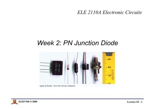
ELE 2110A Electronic Circuits<br />
<strong>Week</strong> 2: <strong>PN</strong> <strong>Junction</strong> <strong>Diode</strong><br />
ELE2110A © 2008<br />
Lecture 02 - 1
Topics to cover…<br />
• Physical operation of pn junction diode<br />
• Terminal I-V characteristics<br />
• Breakdown and junction capacitances<br />
• <strong>Diode</strong> circuits analysis<br />
• Reading Assignment: Chap 3.1-3.7, 3.10-3.13 of Jaeger & Blalock<br />
ELE2110A © 2008<br />
Lecture 02 - 2
Why diodes?<br />
• R, C, L are linear circuit elements<br />
• Many signal processing functions need nonlinear<br />
elements, like signal rectification (to<br />
convert negative signal to be positive).<br />
Nonlinear signal processing<br />
An AC-DC converter<br />
ELE2110A © 2008<br />
Lecture 02 - 3
Why diodes?<br />
• Basic function of diode: to allow current to flow only in<br />
one direction.<br />
<strong>Diode</strong> symbol<br />
• Applications:<br />
– Rectifiers<br />
– Waveform clipping and clamping circuits<br />
– DC-DC converters<br />
Waveform clipping<br />
Waveform clamping<br />
ELE2110A © 2008<br />
Lecture 02 - 4
Physical Structure of pn <strong>Junction</strong> <strong>Diode</strong><br />
Metal<br />
Contact<br />
p-type<br />
n-type<br />
<strong>Diode</strong> symbol<br />
Note:<br />
both p and n regions<br />
are charge neutral.<br />
ELE2110A © 2008<br />
Lecture 02 - 5
Diffusion of Electrons and Holes<br />
• Electrons tend to diffuse from n side to p side<br />
• Holes tend to diffuse from p side to n side<br />
• The resulted current is diffuse current. It is due to the<br />
movement of majority carriers.<br />
• Q: What are the directions of electron and hole diffusion<br />
currents?<br />
ELE2110A © 2008<br />
Lecture 02 - 6
Diffusion of Electrons and Holes<br />
• If diffusion processes were to continue unabated, there<br />
would eventually be a uniform distribution of electrons<br />
and holes.<br />
• But there is a counter force…<br />
ELE2110A © 2008<br />
Lecture 02 - 7
Formation of Depletion Region<br />
Holes and electrons<br />
are depleted from the<br />
dopant atoms<br />
ELE2110A © 2008<br />
Lecture 02 - 8
Built-in Electric Field<br />
Charge Density Electric Field Potential<br />
ρ<br />
∇⋅E<br />
= ε<br />
E(x) = 1 ε s<br />
∫<br />
s<br />
(Gauss’ Law)<br />
ρ(x)dx<br />
E(x)=-∇φ(x)<br />
φ<br />
−∫<br />
= E(<br />
x dx<br />
j<br />
)<br />
built-in<br />
potential<br />
(1 dimension)<br />
Solid-state physics tells us that:<br />
A<br />
=<br />
2<br />
q ni<br />
The resulting potential gives rise to drift currents.<br />
φ<br />
j<br />
kT ⎛ N<br />
ln<br />
⎜<br />
⎝<br />
N<br />
D<br />
⎞<br />
⎟<br />
⎠<br />
ELE2110A © 2008<br />
Lecture 02 - 9
Built-in Electric Field<br />
Charge Density Electric Field Potential<br />
Direction of drift current:<br />
built-in<br />
potential<br />
Drift current is due to the movement of minorities.<br />
For a diode with no external connections, the total current through it must<br />
be zero. Therefore, under thermal equilibrium (no external voltage), drift<br />
and diffusion currents have the same magnitude but opposite direction.<br />
ELE2110A © 2008<br />
Lecture 02 - 10
Width of Depletion Region<br />
Charge Density Electric Field Potential<br />
E(x) = 1 ε s<br />
∫<br />
ρ(x)dx<br />
φ<br />
−∫<br />
= E(<br />
x dx<br />
j<br />
)<br />
Depletion width is an important device parameter.<br />
It can be shown that:<br />
φ<br />
j<br />
built-in<br />
potential<br />
kT ⎛ N<br />
ln<br />
⎜<br />
⎝<br />
N<br />
A<br />
=<br />
2<br />
q ni<br />
D<br />
⎞<br />
⎟<br />
⎠<br />
w d0 = (x n + x p ) =<br />
2ε s<br />
q<br />
⎛ 1<br />
⎜ + 1<br />
⎝ N A<br />
N D<br />
⎞<br />
⎟ φ j<br />
⎠<br />
ELE2110A © 2008<br />
Lecture 02 - 11
Forward-Biased <strong>PN</strong> <strong>Junction</strong><br />
Forward biasing means applying an external voltage v D > 0:<br />
• Built-in potential drops (barrier lowers)<br />
• Majority electrons and holes easily cross the junction<br />
• Balance between diffusion and drift breaks<br />
• Current appears at the terminals:<br />
i D = I diffusion –I drift > 0<br />
In fact, I diffusion increases exponentially with V D .<br />
ELE2110A © 2008<br />
Lecture 02 - 12
Reverse-Biased <strong>PN</strong> <strong>Junction</strong><br />
Reverse biasing means applying an external voltage v D < 0:<br />
• Built-in potential increases/barrier increases;<br />
• Majority electrons and holes can hardly cross the junction<br />
– Diffusion decreases<br />
• Drift current almost unchanged as there are little supply of carriers<br />
(minorities).<br />
∴ i D = I diffusion –I drift < 0 and tends to –I drift .<br />
ELE2110A © 2008<br />
Lecture 02 - 13
Topics to cover…<br />
• Physical operation of pn junction diode<br />
• Terminal I-V characteristics<br />
• Breakdown and junction capacitances<br />
• <strong>Diode</strong> circuits analysis<br />
ELE2110A © 2008<br />
Lecture 02 - 14
<strong>Diode</strong> Terminal I-V Characteristics<br />
i<br />
D<br />
⎡ ⎛ v ⎞ ⎤<br />
D<br />
= I ⎢exp<br />
⎜<br />
⎟ −1<br />
S<br />
⎥<br />
⎢⎣<br />
⎝ VT<br />
⎠ ⎥⎦<br />
where I S = reverse saturation current [A]<br />
v D = voltage applied to diode [V]<br />
V T = kT/q = thermal voltage [V] (25 mV at<br />
room temp.)<br />
q = electronic charge [1.60 x 10 -19 C]<br />
k = Boltzmann’s constant [1.38 x 10 -23<br />
J/K]<br />
T = absolute temperature [K]<br />
ELE2110A © 2008<br />
Lecture 02 - 15
<strong>Diode</strong> Current for Reverse, Zero, and<br />
Forward Bias<br />
• Reverse bias:<br />
⎡ ⎛ v ⎞ ⎤<br />
D<br />
iD<br />
= I<br />
S ⎢exp<br />
⎜ ⎥ ≈ I<br />
S<br />
−<br />
⎣ V<br />
⎟ − 1 0 1<br />
⎝ T ⎠ ⎦<br />
• Zero bias:<br />
D<br />
• Forward bias:<br />
i<br />
D<br />
=<br />
I<br />
S<br />
i<br />
I<br />
[ ] ≈ −I<br />
S<br />
⎡ ⎛ v ⎞ ⎤<br />
D<br />
⎢exp ⎜<br />
⎟ −1⎥<br />
= I =<br />
⎣ ⎝ VT<br />
⎠ ⎦<br />
=<br />
S<br />
S<br />
⎡ ⎛ v<br />
⎢exp<br />
⎜<br />
⎣ ⎝ V<br />
D<br />
T<br />
⎞ ⎤<br />
⎟ −1⎥<br />
⎠ ⎦<br />
≈<br />
I<br />
S<br />
⎛ v<br />
exp<br />
⎜<br />
⎝ V<br />
[ 1−1] 0<br />
D<br />
T<br />
⎞<br />
⎟<br />
⎠<br />
for v < −4<br />
D<br />
V T<br />
for vD > 4V T<br />
ELE2110A © 2008<br />
Lecture 02 - 16
Example 1<br />
Problem: Find diode voltage for diode with given specifications<br />
Given data: I S =0.1 fA, I D = 300 µA / 1mA<br />
Assumptions: Room-temperature dc operation with V T =25mV<br />
Analysis:<br />
With I S =0.1 fA, I D = 300 µA<br />
V<br />
D<br />
= V<br />
T<br />
⎛ ⎞<br />
⎜ I ⎟<br />
ln 1+<br />
= (0.025V)ln(1+<br />
3×<br />
10 -4 ) 0.718V<br />
10 -16 A<br />
⎜ ⎟<br />
=<br />
⎜ ⎟<br />
I D<br />
A<br />
⎝ S ⎠<br />
With I D = 1 mA, I S =0.1 fA<br />
V<br />
D<br />
=0.748V<br />
ELE2110A © 2008<br />
Lecture 02 - 17
<strong>Diode</strong> i-v Characteristics<br />
Turn-on voltage marks point of significant current flow.<br />
I s : reverse saturation current<br />
ELE2110A © 2008<br />
Lecture 02 - 18
Semi-log Plot of <strong>Diode</strong> Current<br />
i<br />
D<br />
= I<br />
S<br />
⎛ v<br />
exp<br />
⎜<br />
⎝ V<br />
D<br />
T<br />
⎞<br />
⎟<br />
⎠<br />
i ⎛<br />
D<br />
vD1<br />
− vD<br />
2<br />
Let = exp<br />
⎜<br />
iD<br />
2 ⎝ VT<br />
⎞<br />
⎟<br />
⎠<br />
1<br />
=<br />
10<br />
v<br />
D1<br />
−<br />
v<br />
D2<br />
= V<br />
T<br />
= 2.3V<br />
ln10<br />
T<br />
≈ 60 mV<br />
ELE2110A © 2008<br />
Lecture 02 - 19
Current for Three Different Values of I S<br />
I =10 I = 100I<br />
SA<br />
SB<br />
SC<br />
i<br />
D<br />
=<br />
I<br />
S<br />
⎛ v<br />
exp<br />
⎜<br />
⎝ V<br />
D<br />
T<br />
⎞<br />
⎟<br />
⎠<br />
Let i DA =i DB<br />
i<br />
i<br />
SA<br />
SB<br />
=<br />
⎛ v ⎞<br />
DB<br />
− vDA<br />
exp ⎜<br />
⎟ = 10<br />
⎝ VT<br />
⎠<br />
v<br />
DB<br />
− v<br />
DA<br />
= V<br />
T<br />
ln10<br />
≈<br />
60<br />
mV<br />
ELE2110A © 2008<br />
Lecture 02 - 20
Topics to cover…<br />
• Physical operation of pn junction diode<br />
• Terminal I-V characteristics<br />
• Breakdown and junction capacitances<br />
• <strong>Diode</strong> circuits analysis<br />
ELE2110A © 2008<br />
Lecture 02 - 21
Reverse Breakdown<br />
Breakdown region:<br />
Rapid increase in I D when<br />
reverse bias voltage exceeds<br />
a break down voltage V Z<br />
Typical value of V z :<br />
2 V < V Z < 2000 V<br />
Temp. Coeff.<br />
ELE2110A © 2008<br />
Lecture 02 - 22
Breakdown Mechanism 1: Avalanche Breakdown<br />
• Carriers in the SCR are accelerated by the internal electric field and<br />
collide with fixed atoms<br />
• As the reverse bias increases, the energy of the accelerated carriers<br />
increases, eventually breaking covalent bonds and generating<br />
electron-hole pairs<br />
• The newly created carriers also accelerate, collide with atoms, and<br />
generate other electron-hole pairs. This process feeds on itself and<br />
leads to avalanche breakdown<br />
• Si diodes with V Z > 5.6 V enter breakdown through this mechanism<br />
ELE2110A © 2008<br />
Lecture 02 - 23
Breakdown Mechanism 2: Zener Breakdown<br />
• Zener breakdown: occurs when the electric field in the depletion<br />
region increases to the point where it can break covalent bonds and<br />
generate electron-hole pairs.<br />
• V Z < 5.6 V for diodes entering breakdown through this mechanism<br />
• In avalanche breakdown, V Z increases with temperature<br />
• In Zener breakdown, V Z decreases with temperature<br />
• Breakdown is not a destructive process provided that the maximum<br />
specified power dissipation is not exceeded<br />
ELE2110A © 2008<br />
Lecture 02 - 24
pn <strong>Junction</strong> Capacitance: Reverse Bias<br />
• External reverse bias leads to:<br />
– Increases of the built-in potential<br />
– Increases of the SCR, and thus fixed space charges<br />
• This behaviors like a capacitor, and is referred to as<br />
depletion capacitance.<br />
ELE2110A © 2008<br />
Lecture 02 - 25
pn <strong>Junction</strong> Capacitance: Forward Bias<br />
Forward bias minority distribution in neutral regions<br />
ELE2110A © 2008<br />
Lecture 02 - 26
pn <strong>Junction</strong> Capacitance: Forward Bias<br />
Excess charge stored in neutral region near edges of space charge<br />
region is<br />
Q<br />
=<br />
D<br />
i D<br />
τ<br />
T<br />
Coulombs<br />
t T is called diode transit time and depends on size and type of diode.<br />
The Q depends on i D and in turn on v D . This capacitance behavior is<br />
referred to as diffusion capacitance and given by:<br />
C<br />
j<br />
=<br />
dQ<br />
dv<br />
D<br />
D<br />
=<br />
dQ<br />
di<br />
D<br />
D<br />
di<br />
dv<br />
D<br />
D<br />
≅<br />
iDτ<br />
T<br />
V<br />
T<br />
[F]<br />
i<br />
D<br />
=<br />
I<br />
S<br />
⎡ ⎛ v<br />
⎢exp<br />
⎜<br />
⎣ ⎝ V<br />
D<br />
T<br />
⎞ ⎤<br />
⎟ − 1⎥<br />
⎠ ⎦<br />
≈<br />
I<br />
S<br />
⎛ v<br />
exp<br />
⎜<br />
⎝ V<br />
D<br />
T<br />
⎞<br />
⎟<br />
⎠<br />
Diffusion capacitance is proportional to current and becomes quite<br />
large at high currents.<br />
ELE2110A © 2008<br />
Lecture 02 - 27
<strong>Diode</strong> Circuit Analysis: Basics<br />
Objective: to find the DC current (I D ) and voltage (V D ), or quiescent<br />
operating point (Q-point) of the diode.<br />
V and R may represent<br />
Thevenin equivalent of a<br />
more complex 2-terminal<br />
network.<br />
Full set of equations:<br />
1. <strong>Diode</strong> equation:<br />
I<br />
D<br />
⎡ ⎛V<br />
⎞ ⎤<br />
D<br />
= I ⎢<br />
⎜<br />
⎟ −<br />
S<br />
exp 1⎥<br />
⎣ ⎝ VT<br />
⎠ ⎦<br />
2. KVL along the loop:<br />
V = I R +<br />
D<br />
V D<br />
nonlinear<br />
This is also called the load line<br />
equation of the diode, as if the<br />
V-source and R were the load of the<br />
diode.<br />
ELE2110A © 2008<br />
Lecture 02 - 28
Topics to cover…<br />
• Physical operation of pn junction diode<br />
• Terminal I-V characteristics<br />
• Breakdown and junction capacitances<br />
• <strong>Diode</strong> circuits analysis<br />
ELE2110A © 2008<br />
Lecture 02 - 29
<strong>Diode</strong> Circuit Analysis Approaches<br />
• Graphical analysis (load-line method)<br />
• Numerical Analysis with diode’s mathematical model<br />
• Simplified analysis with ideal diode model.<br />
• Simplified analysis using constant voltage drop model.<br />
ELE2110A © 2008<br />
Lecture 02 - 30
Load-Line Analysis (Example 2)<br />
Problem: Find Q-point<br />
Given data: V=10 V, R=10kΩ.<br />
<strong>Diode</strong> I-V curve.<br />
Analysis:<br />
4<br />
10 = I<br />
D10<br />
+ V D<br />
To define the load line we use,<br />
VD<br />
= 0, I<br />
D<br />
= (10V /10kΩ)<br />
=<br />
V = 5, I = 0.5 mA<br />
D<br />
D<br />
These points and the resulting load<br />
line are plotted. Q-point is given by<br />
intersection of load line and diode<br />
characteristic:<br />
Q-point = (0.95 mA, 0.6 V)<br />
1mA<br />
ELE2110A © 2008<br />
Lecture 02 - 31
Numerical Analysis (Example 3)<br />
Problem: Find Q-point for given diode characteristics.<br />
Given data: I S =10 -13 A,V T =25 mV, V = 10 V, R = 10kΩ.<br />
Analysis:<br />
⎧I<br />
⎨<br />
⎩<br />
D<br />
=<br />
⇒10<br />
f<br />
= 10<br />
I<br />
S<br />
−13<br />
[ exp( V / V ) −1] = 10 [ exp( 40V<br />
) −1]<br />
4<br />
= 10 10<br />
−10<br />
−9<br />
D<br />
−13<br />
10<br />
T<br />
=<br />
I<br />
D<br />
10<br />
+ V<br />
D<br />
[ exp( 40V<br />
D<br />
) −1] + VD<br />
This is a transcendental equation and does not have analytical<br />
solutions. A numerical answer can be found by using Newton’s iterative<br />
method.<br />
Let:<br />
We desire to find V D for which f=0.<br />
[ exp( 40V ) ] D<br />
−1<br />
−VD<br />
4<br />
D<br />
ELE2110A © 2008<br />
Lecture 02 - 32
Newton’s Iteration Method for f (v D ) = 0<br />
1. Make initial guess V D<br />
0<br />
2. Evaluate f and its derivative f ’ for this value of V D<br />
3. Calculate new guess for V D using<br />
4. Repeat steps 2 and 3 till convergence<br />
V<br />
1<br />
D<br />
= V<br />
0<br />
D<br />
−<br />
f<br />
( )<br />
0<br />
V<br />
f '(<br />
V<br />
D<br />
0<br />
D<br />
)<br />
f<br />
'<br />
( ) ( )<br />
0<br />
f VD<br />
V =<br />
0 − 0<br />
D<br />
0 1<br />
VD<br />
−VD<br />
ELE2110A © 2008<br />
Lecture 02 - 33
Solution from a Spreadsheet<br />
Iteration # V_D [V] f<br />
f'<br />
I_D [A]<br />
0 0.8000 -7.895E+04 -3.159E+06 7.896E+00<br />
1 0.7750 -2.904E+04 -1.162E+06 2.905E+00<br />
2 0.7500 -1.068E+04 -4.276E+05 1.069E+00<br />
3 0.7250 -3.927E+03 -1.575E+05 3.936E-01<br />
4 0.7001 -1.442E+03 -5.806E+04 1.452E-01<br />
5<br />
0.6753<br />
-5.281E+02<br />
-2.150E+04<br />
5.374E-02<br />
6<br />
0.6507<br />
-1.918E+02<br />
-8.048E+03<br />
2.012E-02<br />
7<br />
0.6269<br />
-6.817E+01<br />
-3.103E+03<br />
7.754E-03<br />
8<br />
0.6049<br />
-2.281E+01<br />
-1.289E+03<br />
3.220E-03<br />
9<br />
0.5872<br />
-6.455E+00<br />
-6.357E+02<br />
1.587E-03<br />
10<br />
0.5770<br />
-1.148E+00<br />
-4.238E+02<br />
1.057E-03<br />
11<br />
0.5743<br />
-5.989E-02<br />
-3.804E+02<br />
9.486E-04<br />
12<br />
13<br />
0.5742<br />
0.5742<br />
-1.876E-04<br />
-1.858E-09<br />
-3.780E+02<br />
-3.780E+02<br />
9.426E-04<br />
9.426E-04<br />
Q-point<br />
ELE2110A © 2008<br />
Lecture 02 - 34
Analysis using Ideal <strong>Diode</strong> Model<br />
Ideal diode model:<br />
Forward-biased: voltage = zero, i D >0<br />
Reverse-biased: current = zero, v D
Example 4<br />
Since source is forcing positive current through diode, assume<br />
diode is on. So V D =0.<br />
(10 − 0)V<br />
I D<br />
= = 1 mA<br />
10kΩ<br />
Since I D > 0, our assumption is correct.<br />
Q-point is (1 mA, 0V).<br />
ELE2110A © 2008<br />
Lecture 02 - 36
Example 5<br />
Since source is forcing current backward through diode,<br />
assume diode is off. Hence I D =0.<br />
10 + V<br />
∴V<br />
D<br />
D<br />
+ 10<br />
4<br />
= −10V<br />
I<br />
D<br />
=<br />
0<br />
Since V D < 0, our assumption is right.<br />
Q-point is (0, -10 V)<br />
ELE2110A © 2008<br />
Lecture 02 - 37
Constant Voltage Drop Model<br />
Forward-bias: v D = V on , i D >0<br />
Reverse-bias: i D = 0, v D < V on<br />
ELE2110A © 2008<br />
Lecture 02 - 38
Example 6<br />
Analysis:<br />
Since 10V source is forcing positive current through<br />
diode, we assume diode is on.<br />
I<br />
D<br />
=<br />
(10 −V<br />
)V<br />
10kΩ<br />
(10 − 0.6)V<br />
10kΩ<br />
=<br />
on<br />
=<br />
0.94mA<br />
Since I D > 0, our assumption is correct.<br />
Q-point is (0.94 mA, 0.6V).<br />
ELE2110A © 2008<br />
Lecture 02 - 39
Two-<strong>Diode</strong> Circuit Analysis (Example 7)<br />
Analysis:<br />
Choose ideal diode model.<br />
Assume both diodes are on.<br />
Since V D1<br />
=0,<br />
I<br />
=<br />
(15 − 0)V<br />
10kΩ<br />
1<br />
=<br />
1.50mA<br />
I 0 − ( −10)<br />
V<br />
=<br />
2.<br />
00 mA<br />
D2<br />
5 kΩ<br />
=<br />
I = I −I<br />
= 1.5−2=−0.5 mA<br />
D1<br />
1 D2<br />
Q-points are (-0.5mA, 0V) and (2.0mA, 0V)<br />
But, I D1<br />
Example 7 (Cont.)<br />
The second guess is D 1<br />
off and D 2 on:<br />
Since I D2 = I 1 ,<br />
15−(<br />
−10)<br />
I =<br />
1 10kΩ+<br />
5kΩ<br />
= 1.67mA<br />
V = 15−10,000I<br />
=−1.67V<br />
D1<br />
1<br />
Q-points are D 1 : (0 mA, -1.67 V): off<br />
D 2 : (1.67 mA, 0 V) : on<br />
This is consistent with our assumptions and analysis is finished.<br />
ELE2110A © 2008<br />
Lecture 02 - 41
Breakdown Region <strong>Diode</strong> Model<br />
In breakdown, the diode is modeled with a DC voltage source, V Z , and<br />
a series resistance, R Z . R Z models the slope of the i-v characteristic.<br />
<strong>Diode</strong>s designed to operate in reverse breakdown are called Zener<br />
diodes and use the indicated symbol<br />
ELE2110A © 2008<br />
Lecture 02 - 42
Zener <strong>Diode</strong> Circuit Analysis<br />
(Example 8)<br />
Load-line equation :<br />
(KVL along the loop)<br />
V<br />
D<br />
+ 5000 I + 20=<br />
0<br />
D<br />
Using graphic analysis:<br />
Choose 2 points (0V, -4mA) and<br />
(-5V, -3mA) to draw the load line.<br />
It intersects with i-v characteristic at<br />
Q-point (-2.9 mA, -5.2 V).<br />
ELE2110A © 2008<br />
Lecture 02 - 43
Zener <strong>Diode</strong> Circuit Analysis<br />
(Example 9)<br />
Using piecewise linear model:<br />
I<br />
Z<br />
= −I<br />
>0<br />
D<br />
Assume in breakdown region<br />
−20+<br />
5100I<br />
+ 5=<br />
0<br />
Z<br />
(20−5)V<br />
I = = 2.94mA<br />
Z 5100Ω<br />
Since I Z >0 (I D
Zener <strong>Diode</strong> Applications: Voltage Regulator<br />
ELE2110A © 2008<br />
Lecture 02 - 45
Zener <strong>Diode</strong> Applications: Voltage Regulator<br />
Use constant voltage drop model:<br />
I<br />
S<br />
I<br />
L<br />
I<br />
Z<br />
V<br />
= S<br />
V<br />
=<br />
Z<br />
R<br />
L<br />
I<br />
=<br />
−V<br />
Z<br />
R<br />
(20−5)V<br />
= = 3mA<br />
5kΩ<br />
5V<br />
= = 1mA<br />
5kΩ<br />
−<br />
S<br />
I<br />
L<br />
=2mA<br />
Zener diode keeps voltage<br />
across load resistor constant<br />
ELE2110A © 2008<br />
∴I<br />
Z<br />
For proper regulation, I Z >0 . If I Z < 0,<br />
Zener diode no longer controls voltage<br />
across load resistor and the regulator is<br />
said to have “dropped out of<br />
regulation”.<br />
V<br />
=<br />
S<br />
R<br />
−V<br />
Z<br />
⎛<br />
⎜<br />
⎜<br />
⎜<br />
⎝<br />
⎞<br />
1 + 1<br />
⎟<br />
⎟<br />
> 0<br />
R R ⎟<br />
L ⎠<br />
R > R = R<br />
L ⎛V<br />
min<br />
1<br />
V S<br />
⎞<br />
⎜ ⎟<br />
⎜ − ⎟<br />
⎜ ⎟<br />
⎝ Z ⎠<br />
Lecture 02 - 46
Example 10<br />
Zener diode model<br />
Analysis:<br />
KCL at output node:<br />
V<br />
L<br />
− 20<br />
5000<br />
VL<br />
− 5<br />
+<br />
100<br />
+<br />
V<br />
L<br />
5000<br />
=<br />
0<br />
Problem: Find V L and I Z using the<br />
piece-wise linear model.<br />
Given data:<br />
V S =20 V, R=5 kΩ,<br />
R Z =0.1 kΩ, V Z =5 V<br />
I<br />
Z<br />
∴ V =5.19V L<br />
V −5<br />
= L = 5.19 − 1.9mA 0<br />
100 100 5 = ><br />
<strong>Diode</strong> is actually operating in<br />
breakdown region as assumed.<br />
ELE2110A © 2008<br />
Lecture 02 - 47
Line and Load Regulation<br />
Load is modeled<br />
as an I-source<br />
By superposition:<br />
Line regulation ≡<br />
∂V<br />
∂V<br />
L<br />
S<br />
R<br />
z<br />
V<br />
L<br />
= VZ<br />
+ VS<br />
− ( Rz<br />
// R)<br />
R + Rz<br />
R + Rz<br />
=<br />
R<br />
R<br />
+<br />
z<br />
R<br />
z<br />
R<br />
(characterizes how sensitive output<br />
voltage is to input voltage changes)<br />
I<br />
L<br />
Load<br />
regulation<br />
≡<br />
∂V<br />
∂I<br />
L<br />
L<br />
=<br />
−( R // R) [ Ω]<br />
z<br />
(characterizes how sensitive output<br />
voltage is to load current changes)<br />
ELE2110A © 2008<br />
Lecture 02 - 48