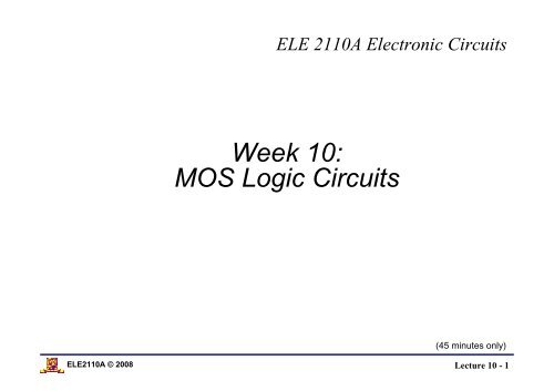
Week 10: MOS Logic Circuits
Week 10: MOS Logic Circuits
Week 10: MOS Logic Circuits
You also want an ePaper? Increase the reach of your titles
YUMPU automatically turns print PDFs into web optimized ePapers that Google loves.
ELE 21<strong>10</strong>A Electronic <strong>Circuits</strong><br />
<strong>Week</strong> <strong>10</strong>:<br />
<strong>MOS</strong> <strong>Logic</strong> <strong>Circuits</strong><br />
(45 minutes only)<br />
ELE21<strong>10</strong>A © 2008<br />
Lecture <strong>10</strong> - 1
• C<strong>MOS</strong> Inverter<br />
– Static characteristics<br />
– Dynamic characteristics<br />
– Power dissipation<br />
• Other C<strong>MOS</strong> logic gates<br />
Topics to cover …<br />
Reading Assignment:<br />
Chap 6.1-6.3, 7.1-7.4 of Jaeger and Blalock or<br />
Chap 7.1 - 7.3, 7.7 of Sedra and Smith<br />
ELE21<strong>10</strong>A © 2008<br />
Lecture <strong>10</strong> - 2
Digital IC Technologies and <strong>Logic</strong>-Circuit Family<br />
Digital IC technologies & logic circuit family<br />
C<strong>MOS</strong> Bipolar BiC<strong>MOS</strong> GaAs<br />
C<strong>MOS</strong><br />
This course<br />
Pseudo<br />
-N<strong>MOS</strong><br />
Pass<br />
Transistor<br />
<strong>Logic</strong><br />
Dynamic<br />
<strong>Logic</strong><br />
Transistor-<br />
Transistor<br />
<strong>Logic</strong> (TTL)<br />
Emitter<br />
Coupled<br />
<strong>Logic</strong><br />
(ECL)<br />
ELE21<strong>10</strong>A © 2008<br />
Lecture <strong>10</strong> - 3
Ideal Inverter<br />
V O<br />
V OH<br />
=V DD<br />
V OL<br />
=0<br />
V DD<br />
/2<br />
V DD<br />
V I<br />
The Voltage Transfer<br />
Characteristic (VTC)<br />
of an ideal inverter<br />
ELE21<strong>10</strong>A © 2008<br />
Lecture <strong>10</strong> - 4
C<strong>MOS</strong> Inverter<br />
pmos<br />
nmos<br />
PU: pull up network, responsible for producing HIGH output<br />
PD: pull down network, responsible for producing LOW output<br />
ELE21<strong>10</strong>A © 2008<br />
Lecture <strong>10</strong> - 5
Case 1: V I =V DD<br />
)<br />
“pull-down”<br />
Q P<br />
OFF<br />
Q N<br />
ON: output pulled down<br />
V O<br />
=0V<br />
The output resistance of Q N<br />
(linear mode):<br />
r<br />
DSN<br />
=<br />
⎛<br />
k ′<br />
n ⎜<br />
⎝<br />
W<br />
L<br />
1<br />
⎞<br />
⎟(<br />
V<br />
⎠<br />
DD<br />
− V<br />
tn<br />
ELE21<strong>10</strong>A © 2008<br />
Lecture <strong>10</strong> - 6
Case 2: V I = 0V<br />
“pull-up”<br />
Q N<br />
OFF<br />
Q P<br />
ON: output pulled up.<br />
The output resistance of Q P<br />
(linear mode):<br />
r<br />
DSN<br />
=<br />
→V O<br />
=V DD<br />
)<br />
k ′<br />
p<br />
⎛ W<br />
⎜<br />
⎝ L<br />
1<br />
⎞<br />
⎟(<br />
V<br />
⎠<br />
DD<br />
− V<br />
tp<br />
ELE21<strong>10</strong>A © 2008<br />
Lecture <strong>10</strong> - 7
• C<strong>MOS</strong> Inverter<br />
– Static characteristics<br />
– Dynamic characteristics<br />
– Power dissipation<br />
• Other C<strong>MOS</strong> logic gates<br />
Topics to cover …<br />
ELE21<strong>10</strong>A © 2008<br />
Lecture <strong>10</strong> - 8
Dynamic Characteristic: Rise and Fall times<br />
• The rise and fall times, t f and t r ,<br />
are measured at the <strong>10</strong>% and<br />
90% points on the transitions<br />
between the two states.<br />
V <strong>10</strong>% = V L + 0.1∆V<br />
V 90% = V L + 0.9∆V<br />
= V H – 0.1∆V<br />
ELE21<strong>10</strong>A © 2008<br />
Lecture <strong>10</strong> - 9
Dynamic Characteristic: Propagation Delay<br />
• Propagation delay: the time between<br />
a change at the 50% point input to<br />
cause a change at the 50% point of<br />
the output<br />
• The high-to-low prop delay, τ PHL<br />
, and<br />
the low-to-high prop delay, τ PLH<br />
, are<br />
usually not equal, but can be<br />
described as an average value:<br />
τ<br />
P<br />
τ<br />
=<br />
PHL<br />
+ τ<br />
2<br />
PLH<br />
ELE21<strong>10</strong>A © 2008<br />
Lecture <strong>10</strong> - <strong>10</strong>
Propagation Delay<br />
• C represents parasitic capacitances:<br />
– <strong>MOS</strong> gate capacitance of next logic gate<br />
– Wire capacitance to ground<br />
• Output parasitic capacitor voltage cannot change instantaneously<br />
• Capacitive charging/discharging contributes to propagation delay<br />
ELE21<strong>10</strong>A © 2008<br />
Lecture <strong>10</strong> - 11
Propagation Delay Estimate<br />
• It can be shown (see section 7.3.1 and 6.14.12)<br />
τ<br />
PHL<br />
∝<br />
where<br />
R<br />
R<br />
onN<br />
onN<br />
µ<br />
nCox<br />
( VH<br />
−VTN<br />
)<br />
⎛W<br />
⎞<br />
µ C ⎜ ⎟ = µ<br />
⎝ L ⎠ n<br />
• The delay also depends on R ON<br />
C<br />
=<br />
• For matched nmos and pmos ( n ox<br />
p ox ), τ PLH = τ PHL<br />
W<br />
L<br />
• The delay depends on C<br />
– In smaller feature size C<strong>MOS</strong> process, wires and transistors are smaller<br />
– Parasitic C is smaller<br />
– Delay is smaller <strong>Circuits</strong> run faster<br />
1<br />
C<br />
⎛ W ⎞<br />
⎜ ⎟<br />
⎝ L ⎠<br />
p<br />
ELE21<strong>10</strong>A © 2008<br />
Lecture <strong>10</strong> - 12
Example<br />
Given that:<br />
For C=1pF,<br />
τ<br />
p<br />
= 6. 4ns<br />
τ = ?<br />
τ p<br />
= ?<br />
p<br />
ELE21<strong>10</strong>A © 2008<br />
Lecture <strong>10</strong> - 13
Ring Oscillator<br />
1 2 3 4 5 6<br />
To OSC input<br />
• If odd number of inverters (at least 3) are connected as a ring, it<br />
oscillates.<br />
• Oscillation frequency relates to the propagation delay of the inverters<br />
• Waveform at 6 = waveform at 1 5 Delays = T/2 Delay = T/<strong>10</strong><br />
At 1<br />
At 2<br />
At 3<br />
At 4<br />
At 5<br />
At 6<br />
T/2<br />
T<br />
0V<br />
ELE21<strong>10</strong>A © 2008<br />
Lecture <strong>10</strong> - 14
• C<strong>MOS</strong> Inverter<br />
– Static characteristics<br />
– Dynamic characteristics<br />
– Power dissipation<br />
• Other C<strong>MOS</strong> logic gates<br />
Topics to cover …<br />
ELE21<strong>10</strong>A © 2008<br />
Lecture <strong>10</strong> - 15
Power Dissipation<br />
• C<strong>MOS</strong> logic has no static power dissipation<br />
– The is no DC path between VDD and GND at any time<br />
• But, when the inverter changes its output…<br />
ELE21<strong>10</strong>A © 2008<br />
Lecture <strong>10</strong> - 16
Dynamic Power Dissipation<br />
• When the inverter charges or discharges the output capacitor, it<br />
consumes power.<br />
Charging<br />
Discharging<br />
ELE21<strong>10</strong>A © 2008<br />
Lecture <strong>10</strong> - 17
Dynamic Power Dissipation<br />
• The energy delivered from the VDD is:<br />
E<br />
D<br />
∞<br />
∞<br />
VC<br />
( ∞)<br />
dq(<br />
t)<br />
2<br />
= V ∫ DD<br />
i( t)<br />
dt = V ∫ DD<br />
dt = CV ∫ DD<br />
1dvC<br />
= CVDD<br />
dt<br />
0<br />
0<br />
V (0)<br />
• The energy stored by the capacitor is:<br />
E =<br />
D<br />
CV<br />
2<br />
2<br />
DD<br />
• The difference between the above two terms represents the energy<br />
lost in the resistive elements:<br />
C<br />
E = E − E =<br />
L<br />
D<br />
S<br />
CV<br />
2<br />
2<br />
DD<br />
ELE21<strong>10</strong>A © 2008<br />
Lecture <strong>10</strong> - 18
Dynamic Power Dissipation<br />
• The total energy lost in the first charging and discharging of the<br />
capacitor through resistive elements is given by:<br />
2<br />
2<br />
CVDD<br />
CVDD<br />
E<br />
TD<br />
= + =<br />
2 2<br />
CV<br />
2<br />
DD<br />
• For every clock cycle, the dynamic power dissipation is:<br />
P<br />
D<br />
= Energy/Tim e =<br />
CV<br />
2<br />
DD<br />
f<br />
– This result can be extended to a complex digital IC, where<br />
C represents the area of the IC<br />
– Lower V DD<br />
is very effective for reducing power supply<br />
– Reducing C also helps reducing power<br />
ELE21<strong>10</strong>A © 2008<br />
Lecture <strong>10</strong> - 19
• C<strong>MOS</strong> Inverter<br />
– Static characteristics<br />
– Dynamic characteristics<br />
– Power dissipation<br />
• Other C<strong>MOS</strong> logic gates<br />
Topics to cover …<br />
ELE21<strong>10</strong>A © 2008<br />
Lecture <strong>10</strong> - 20
C<strong>MOS</strong> NOR Gate<br />
Pull-up Network:<br />
Y =<br />
AB<br />
Pull-down Network:<br />
Y = A +<br />
B<br />
Y = A +<br />
B<br />
ELE21<strong>10</strong>A © 2008<br />
Lecture <strong>10</strong> - 21
Gate Sizing<br />
• Want to keep the delay times the same as a reference inverter<br />
under the worst case input conditions.<br />
• Consider a two-input NOR gate:<br />
– (W/L) n<br />
should be same as that of the inverter<br />
– (W/L) p<br />
should be twice as large as that of the inverter<br />
Reference Inverter<br />
ELE21<strong>10</strong>A © 2008<br />
Lecture <strong>10</strong> - 22
C<strong>MOS</strong> NAND Gate<br />
Pull-up Network:<br />
Y = A +<br />
Y =<br />
B<br />
Pull-down Network:<br />
AB<br />
Y =<br />
AB<br />
ELE21<strong>10</strong>A © 2008<br />
Lecture <strong>10</strong> - 23


