Flip Chip and Wafer-Level Chip Scale Packaging
Flip Chip and Wafer-Level Chip Scale Packaging
Flip Chip and Wafer-Level Chip Scale Packaging

You also want an ePaper? Increase the reach of your titles
YUMPU automatically turns print PDFs into web optimized ePapers that Google loves.
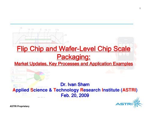
1<br />
<strong>Flip</strong> <strong>Chip</strong> <strong>and</strong> <strong>Wafer</strong>-<strong>Level</strong> <strong>Chip</strong> <strong>Scale</strong><br />
<strong>Packaging</strong>:<br />
Market Updates, Key Processes <strong>and</strong> Application Examples<br />
Dr. Ivan Sham<br />
Applied Science & Technology Research Institute (ASTRI)<br />
Feb. 20, 2009<br />
ASTRI Proprietary
Major References<br />
(33) Overview of ANST, 2008.<br />
(32) International WLP Conference, San Jose, CA, 2008.<br />
(31) Workshop on <strong>Flip</strong> <strong>Chip</strong> Technologies, Prismark, Hong Kong, 2008.<br />
(30) Advanced IC <strong>Packaging</strong>, Electronic Trend Publications, 2007.<br />
(29) Prismark Wireless Technologies Report, 2006, 2007, 2008.<br />
(28) KGD Conference, NAPA, CA 2004 <strong>and</strong> IWLPC, San Jose, CA, 2004.<br />
(27) APiA Seminar, Semicon-West, 2004.<br />
(26) Electronics Manufacturing with Lead-Free Materials, Lau, Wong, Lee & Lee, McGraw-Hill, 2003.<br />
(25) Area Array Interconnection H<strong>and</strong>book, edited by Puttlitz <strong>and</strong> Totta, Kluwer Academic Publishers, 2001.<br />
(24) Low Cost <strong>Flip</strong> <strong>Chip</strong> Technologies, John Lau, McGraw-Hill, 2000.<br />
(23) The International Technology Roadmap for Semiconductors, 1999, 2000, 2001, 2002, 2008 Editions.<br />
(22) <strong>Chip</strong> <strong>Scale</strong> Package, Lau <strong>and</strong> Lee, McGraw-Hill, 1999.<br />
(21) Electronic <strong>Packaging</strong>: Design, Materials, Process, <strong>and</strong> Reliability, Lau, Wong, Prince, <strong>and</strong> Nakayama,<br />
McGraw-Hill, 1998.<br />
(20) Microelectronics <strong>Packaging</strong> H<strong>and</strong>book, edited by Tummala, Rymaszewski, <strong>and</strong> Klopfenstein, second edition,<br />
Chapman & Hall, 1997.<br />
(19) Solder Joint Reliability of BGA, CSP, <strong>Flip</strong> <strong>Chip</strong>, <strong>and</strong> Fine Pitch SMT Assemblies, Lau <strong>and</strong> Pao, McGraw-Hill,<br />
1997.<br />
(18) <strong>Flip</strong> <strong>Chip</strong> Technologies, edited by J. Lau, McGraw-Hill, 1996.<br />
(17) Ball Grid Array Technology, edited by J. Lau, McGraw-Hill, 1995.<br />
(16) <strong>Chip</strong> on Board Technologies for Multichip Modules, edited by J. Lau, Van Nostr<strong>and</strong> Reinhold (VNR), 1994.<br />
(15) H<strong>and</strong>book of Fine Pitch Surface Mount Technology, edited by J. Lau, VNR, 1994.<br />
(14) Multichip Module Technologies <strong>and</strong> Alternatives, edited by Doane <strong>and</strong> Franzon, VNR, 1993.<br />
(13) Surface Mount Technology - Recent Japanese Developments, edited by Jan Vardaman, IEEE Press, 1993.<br />
(12) Thin Film Multichip Modules, edited by Messner, Turlik, Balde, <strong>and</strong> Garrou, International Society for Hybrid<br />
Microelectronics, 1992.<br />
(11) H<strong>and</strong>book of Tape Automated Bonding (TAB), edited by J. Lau, Van Nostr<strong>and</strong> Reinhold, 1992.<br />
(10) Solder Joint Reliability: Theory <strong>and</strong> Applications, edited by J. Lau, VNR, 1991.<br />
(9) Multichip Modules, edited by Johnson, Teng <strong>and</strong> Balde, IEEE Press, 1990.<br />
(8) Surface Mount Technology: Principles <strong>and</strong> Practice, Ray P. Prasad, VNR, 1989.<br />
(7) Microelectronics <strong>Packaging</strong> H<strong>and</strong>book, edited by Tummala <strong>and</strong> Rymaszewski, VNR, 1989.<br />
(6) Electronic Materials H<strong>and</strong>book, Volume 1, ASM International, 1989.<br />
(5) Principles of Electronic <strong>Packaging</strong>, edited by Seraphim, Lasky <strong>and</strong> Li, McGraw-Hill, 1989.<br />
(4) Proceedings of NEPCON West & East, SMI, ECTC, IEMT, IEPS, ICEMCM, ISHM, <strong>and</strong> ITAP.<br />
(3) The National Technology Roadmaps by IPC, NEMI, <strong>and</strong> SIA.<br />
(2) IEEE Transactions on CPMT.<br />
(1) Magazines of EP&P, Surface Mount Technology, Advanced <strong>Packaging</strong>, <strong>and</strong> Circuits Assembly.<br />
ASTRI Proprietary<br />
2
Outline<br />
3<br />
• Executive Summary<br />
• <strong>Flip</strong> <strong>Chip</strong> <strong>Packaging</strong><br />
– Market Updates<br />
– Key Processes<br />
– Application Examples<br />
• <strong>Wafer</strong>-<strong>Level</strong> <strong>Chip</strong>-<strong>Scale</strong> <strong>Packaging</strong><br />
– Market Updates<br />
– Key Processes<br />
– Application Examples<br />
• Summary<br />
ASTRI Proprietary
Executive Summary<br />
4<br />
• This report studies the latest market trends & applications of flip<br />
chip (FC) <strong>and</strong> chip scale packages (CSP). Array package is going to<br />
be the main package format, where FC-CSP, wafer-level CSP, FC-<br />
BGA/PGA/LGA will have the highest growth rates.<br />
• FC is more suitable for high I/Os (>300), high-end, highperformance<br />
–related applications, such as microprocessor, image<br />
processor, etc., whereas WLCSP is suitable for low I/Os (100), solder<br />
bump reliability <strong>and</strong> costs, etc.<br />
ASTRI Proprietary
Summary (1/3)<br />
5<br />
• The market trend, key processes <strong>and</strong><br />
application examples of flip chip package<br />
<strong>and</strong> wafer-level chip scale package have<br />
been reviewed.<br />
• There are differences between FC <strong>and</strong><br />
WLCSP (Please refer to the tables in<br />
following slides).<br />
• The futures of FC would be primarily related<br />
to high pin counts, high performance<br />
applications while WLCSP would be more<br />
suitable for low pin counts, low-cost<br />
applications.<br />
ASTRI Proprietary
Summary (2/3):<br />
WLCSP versus CSP versus <strong>Flip</strong> <strong>Chip</strong><br />
6<br />
Features WLCSP CSP <strong>Flip</strong> <strong>Chip</strong><br />
1. <strong>Packaging</strong> One (<strong>Wafer</strong> <strong>Level</strong> <strong>Packaging</strong>) One (Single <strong>Chip</strong> <strong>Packaging</strong>) Zero (<strong>Chip</strong> Connection)<br />
<strong>Level</strong><br />
2. Types OWRD, RDWE, Leadframe, Rigid or C4, FCOB/DCA, COG, PFC,<br />
OSRD, <strong>and</strong> WARD Flex Interposer E3, etc.<br />
3. Normalized 1.0 < 1.5 1.0<br />
Footprint<br />
4. Typical Bond 0.5 - 0.8 mm 0.5 - 1.0 mm 0.2 - 0.35 mm<br />
Pitch<br />
5. Package 0.3 - 0.7 mm LF: 0.5 - 1.4, IP: 0.8 - 2.0 0.5 - 0.7 mm<br />
Height<br />
6. I/O Capability < 200 (peripheral, full array 400+ (peripheral, full array 3000+ (full array or center<br />
or center depopulated) or center depopulated) depopulated)<br />
7. <strong>Chip</strong> <strong>Wafer</strong> Processing WB, TAB, or FC Bumping (Evaporated, plated,<br />
Connection<br />
printed, stud bump, etc.)<br />
8. Design Issues Escape routing, fan-in pitch, Escape routing, fan-in vs. fan Escape routing, SMD vs.<br />
pad opening, etc. out, pad size, etc. NSMD, die shrinking<br />
9. Assy Issues Solder volume, ball size/ Solder volume, pad size/ Solder volume, underfill,<br />
shape, mass reflow, etc. shape, mass reflow mass reflow etc.<br />
10. H<strong>and</strong>ling Protected, st<strong>and</strong>ardizable Protected, st<strong>and</strong>ardizable Unprotected (wafer,<br />
(wafer, tray, t & r, tube) (tray, tape <strong>and</strong> reel, tube) tray, tape & reel or Gel-pak)<br />
OWRD: On-<strong>Wafer</strong>/<strong>Chip</strong> Redistribution; RDWE: On-<strong>Wafer</strong>/<strong>Chip</strong> Redistribution with Encapsulation<br />
OSRD: ASTRI On-Substrate Proprietary Redistribution; WARD: Wrap-Around & Redistribution
Summary (3/3):<br />
WLCSP versus CSP versus <strong>Flip</strong> <strong>Chip</strong><br />
7<br />
Features WLCSP CSP <strong>Flip</strong> <strong>Chip</strong><br />
11. Reworkability O. K. for > 0.7 mm pitch O. K. for > 0.7 mm pitch O. K. for non-underfilled<br />
chips<br />
12. Thermal Challenging for devices Mainly for low power Challenging for multichip<br />
with > 2 watts devices configuration<br />
13. Electrical Good (key issues: signal/P/G Good (key issues: signal/P/G Excellent (key issues: alpha,<br />
distribution) distribution) particle, ESD, etc.)<br />
14. Testability Challenging Improving, e.g. dual beam Improving, e.g. KGD carrier<br />
contact<br />
technologies<br />
15. Reliability Bump voiding, uniformity, Popcorn, organic contami- <strong>Chip</strong> cracking, bump voiding,<br />
(Package) interfacial integrity, etc. nation, WB, underfill, etc. uniformity, etc.<br />
16. Reliability Solder joint: pad sIze/shape, Solder joint: pad sIze/shape, Underfill volume, cracking,<br />
(Board Assy) volume, surface finishing volume, surface finishing delamination, solder volume<br />
17. Cost (pkg ~$100 to 200/wafer LF: > TSOP, SOJ; IP: 0.8 - 3.5
8<br />
~ END ~<br />
Enquiry/comment/suggestion?<br />
Please contact us at:<br />
E-mail: ivansham@astri.org<br />
Tel: +852-34062709<br />
ASTRI Proprietary