An Ultra Low-power Programmable DSP System for Hearing Aids ...
An Ultra Low-power Programmable DSP System for Hearing Aids ...
An Ultra Low-power Programmable DSP System for Hearing Aids ...

You also want an ePaper? Increase the reach of your titles
YUMPU automatically turns print PDFs into web optimized ePapers that Google loves.
To appear in ICSPAT’99 Proceedings, November 1-4, 1999, Orlando, FL.<br />
<strong>An</strong> <strong>Ultra</strong> <strong>Low</strong>-<strong>power</strong> <strong>Programmable</strong> <strong>DSP</strong> <strong>System</strong> <strong>for</strong> <strong>Hearing</strong><br />
<strong>Aids</strong> and Other Audio Applications<br />
Todd Schneider, Robert Brennan, † Peter Balsiger and † Alexandre Heubi<br />
Dspfactory Ltd.<br />
611 Kumpf Drive, Unit 200<br />
Waterloo, Ontario, N2V 1K8<br />
Canada<br />
Abstract<br />
This paper describes an application specific<br />
signal processor (ASSP) designed <strong>for</strong><br />
miniature, ultra low-<strong>power</strong>, audio signal<br />
processing applications. The ASSP includes<br />
a high-fidelity weighted overlap-add<br />
(WOLA) filterbank, a 16-bit <strong>DSP</strong> core, two<br />
14-bit A/D converters, a 14-bit D/A converter<br />
and a flexible set of peripherals. This<br />
design excels in applications that require<br />
efficient frequency-domain processing of<br />
one or two audio signals.<br />
1. Introduction<br />
For <strong>DSP</strong> designers, ultra low-<strong>power</strong> applications<br />
are extremely demanding. <strong>An</strong> example<br />
low-<strong>power</strong> application is a digital hearing<br />
aid. These devices must (i) consume less<br />
than 1 mW at 1 volt; (ii) fit into the ear canal<br />
(system size less than 6.5 x 3.5 x 2.5 mm);<br />
and (iii) provide sufficient flexibility and<br />
computational <strong>power</strong> to implement dynamic<br />
range compression, noise reduction, directional<br />
processing and other similar algorithms<br />
Raw MIPS is a poor measure of per<strong>for</strong>mance<br />
in such applications. One must consider<br />
the <strong>power</strong> consumed to realize a particular<br />
algorithm [3]. Typically this figure of<br />
merit is expressed in mW/MIPS.<br />
All of these features – miniature size, ultra<br />
low <strong>power</strong> consumption, targeted processing<br />
capability and flexibility make the design<br />
suitable <strong>for</strong> a wide range of portable audio<br />
and sensor signal processing applications.<br />
† Institute of Microtechnology<br />
University of Neuchâtel<br />
Rue A.-L. Breguet 2, 2000 Neuchâtel,<br />
Switzerland<br />
2. Design Overview<br />
Our design evolved from the realization that<br />
a number of signal processing algorithms<br />
utilize filtering as an underlying component.<br />
Dynamic range compression, noise reduction,<br />
directional processing and many other<br />
algorithms can be cast into a filtering<br />
framework. Thus, the basis of the design is<br />
efficient (yet flexible) filtering.<br />
A significant increase in efficiency is<br />
achieved by “coding” filtering in hardware.<br />
A 16-bit <strong>DSP</strong> core controls this filtering<br />
engine and provides the flexibility needed to<br />
support a range of algorithms. A number of<br />
the filtering parameters are adjustable; thus,<br />
the filtering can be easily configured to meet<br />
the needs of many algorithms.<br />
A parallel processing approach is employed:<br />
many <strong>DSP</strong> algorithms employ high-speed<br />
processing that operates at the incoming<br />
sample rate and lower-speed processing that<br />
operates at a frame rate or with slower time<br />
constants. For improved efficiency, the<br />
high-speed data processing is done in dedicated<br />
hardware. <strong>Low</strong>er-speed processing is<br />
implemented on the <strong>DSP</strong> core.<br />
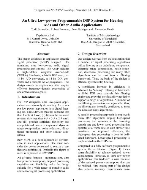
Compared to a fully software-programmable<br />
system, the architecture (Figure 1) trades<br />
some flexibility to achieve reduced <strong>power</strong><br />
consumption. However, in ultra low-<strong>power</strong><br />
applications, this trade-off is wise because<br />
of the reduced <strong>power</strong> consumption that can<br />
be realized. Hard coding part of the design<br />
also reduces memory requirements com-<br />
1
To appear in ICSPAT’99 Proceedings, November 1-4, 1999, Orlando, FL.<br />
pared to that of a fully programmable design<br />
– this further reduces chip size and <strong>power</strong><br />
consumption. Finally, to achieve the lowest<br />
<strong>power</strong> operation, our design operates at 1<br />
volt.<br />
inputs<br />
output<br />
A/D<br />
A/D<br />
D/A<br />
E 2 PROM<br />
input-output<br />
processor<br />
WOLA<br />
filterbank<br />
shared RAM<br />
interface<br />
16-bit Harvard<br />
<strong>DSP</strong> core<br />
peripherals<br />
X,Y,P<br />
SRAM<br />
Figure 1. Block diagram of <strong>DSP</strong> system<br />
The system is implemented on two ASICs.<br />
A digital chip on 0.18 µm CMOS contains<br />
the <strong>DSP</strong> core, RAM and WOLA filterbank<br />
The mixed-signal portions of the design are<br />
implemented on 1 µm CMOS. A separate,<br />
off-the-shelf, E 2 PROM is used <strong>for</strong> nonvolatile<br />
storage.<br />
3. WOLA Filterbank<br />
The filtering specifications <strong>for</strong> the target<br />
real-time audio processing applications are<br />
strict. Specifically, (i) less than 10 ms group<br />
delay, (ii) an adjustable number of bands,<br />
and (iii) at least 50 dB of gain adjustment in<br />
each band are required.<br />
A frequency-domain filterbank was selected<br />
because it offers flexibility and simplified<br />
gain adjustment. Research on these filterbanks<br />
has primarily been done <strong>for</strong> speech<br />
coding applications. In speech coding,<br />
bitrate reduction is the goal; thus, the majority<br />
of these filterbanks use critical sampling<br />
and incorporate alias cancellation to maintain<br />
fidelity.<br />
Simulations showed that large band gain<br />
adjustments (> 20 dB) in a critically sampled<br />
filterbank resulted in severe aliasing<br />
distortion because aliasing cancellation<br />
conditions [8] are violated. Distortion occurs<br />
because imaging in adjacent bands no longer<br />
cancels when the gain is adjusted. By oversampling,<br />
the aliased images are placed<br />
further away from gain adjusted bands so<br />
that they can be rejected by the synthesis<br />
filter.<br />
Figure 2 and Figure 3 show the design of the<br />
analysis and synthesis sections of the<br />
WOLA filterbank [1],[2].<br />
...<br />
input<br />
1 R<br />
sign<br />
X<br />
modulator<br />
1 L<br />
1<br />
L<br />
L<br />
1<br />
N<br />
1<br />
analysis<br />
window<br />
...<br />
+ ... + + + =<br />
0<br />
N/2<br />
band gains<br />
X<br />
X<br />
output<br />
0 N/2<br />
N-point<br />
FFT<br />
Figure 2. WOLA analysis processing<br />
<strong>An</strong>alysis processing (Figure 2) shifts an L-<br />
sample window along the input FIFO, R<br />
samples at a time. Following this, the signal<br />
is “folded,” circularly shifted and processed<br />
with an N-point FFT. Typical values are<br />
R=8, L=128 and N=32, resulting in N/2+1<br />
complex frequency domain values computed<br />
every R samples.<br />
Synthesis processing (Figure 3) is the inverse<br />
of analysis processing. The modified<br />
frequency domain data is processed with an<br />
inverse FFT, circularly shifted and periodically<br />
extended. Then, the synthesis window<br />
is applied and the overlap-add operation is<br />
per<strong>for</strong>med.<br />
shift<br />
2
To appear in ICSPAT’99 Proceedings, November 1-4, 1999, Orlando, FL.<br />
The filterbank oversampling rate (OS) is<br />
OS=N/R (i.e., FFT size / Input block size).<br />
The synthesis window is also decimated by<br />
OS. Thus, oversampling reduces group<br />
delay in two ways: (i) the group delay<br />
through the (FIR) synthesis window is<br />
reduced and (ii) the blocking delay is reduced<br />
when R is shortened. A blocking<br />
delay occurs because the system is reading<br />
an input block, processing a block and<br />
writing an output block simultaneously.<br />
0<br />
N/2<br />
input<br />
1<br />
R<br />
output<br />
N-point<br />
IFFT<br />
X<br />
1<br />
synthesis<br />
window<br />
shift<br />
1 L/OS<br />
periodically extend<br />
X<br />
L/OS<br />
+<br />
1 L/OS<br />
sign<br />
modulator<br />
Figure 3. WOLA synthesis processing<br />
zeros<br />
1 R<br />
The FFT size (N), window length (L) and<br />
input block step size (R) are all adjustable.<br />
Table 1 shows some sample filterbank<br />
configurations and the per<strong>for</strong>mance that can<br />
be realized. Note how reduced group delay<br />
can be “traded” <strong>for</strong> increased <strong>power</strong> consumption,<br />
reduced fidelity (a lower SFDR),<br />
or both.<br />
Table 1. Sample filterbank configurations<br />
(SFDR: spurious-free dynamic range; relative<br />
<strong>power</strong> <strong>for</strong> filterbank only)<br />
Bands<br />
(=N/2)<br />
OS<br />
(=N/R)<br />
Delay<br />
(ms)<br />
Rel.<br />
Power<br />
SFDR<br />
(dB)<br />
16 2 14 1 65<br />
16 4 6 1.5 50<br />
32 4 12 1.6 45<br />
128 1 27 2 40<br />
The WOLA filterbank can operate in either<br />
even or odd stacking (Figure 4). Even<br />
stacking provides N/2+1 bands and is useful<br />
when the highest and lowest half-bands are<br />
not processed. Odd stacking provides N/2<br />
bands and is useful in subband coding,<br />
where equal width bands result in simplified<br />
processing. Both even and odd stacking are<br />
useful in hearing aid applications where<br />
twice the number of band-edges allows a<br />
better fit to “sharp” hearing losses.<br />
Gain (dB)<br />
Gain (dB)<br />
0<br />
-10<br />
-20<br />
-30<br />
-40<br />
Even Stacking<br />
-50<br />
0 1000 2000 3000 4000 5000 6000 7000 8000<br />
Frequency (Hz)<br />
0<br />
-10<br />
-20<br />
-30<br />
-40<br />
Odd Stacking<br />
-50<br />
0 1000 2000 3000 4000 5000 6000 7000 8000<br />
Frequency (Hz)<br />
Figure 4. Frequency responses <strong>for</strong> even and odd<br />
stacking (16-channels, τ = 6 ms, f s = 16 kHz)<br />
In stereo processing mode, the WOLA<br />
filterbank treats two real signals as a single<br />
complex signal. After filterbank processing,<br />
the two signals are separated by the core in a<br />
known manner [6]. Stereo mode is useful <strong>for</strong><br />
directional processing because it provides<br />
magnitude and phase in<strong>for</strong>mation <strong>for</strong> both<br />
input signals.<br />
The WOLA interfaces to the <strong>DSP</strong> core via<br />
shared memory. Communication is via a<br />
control register and interrupts. The design<br />
supports concurrent processing on the<br />
WOLA and <strong>DSP</strong> core.<br />
Within the WOLA, block floating-point<br />
arithmetic, with greater than 16-bits precision,<br />
is used to maintain fidelity. This provides<br />
more than 100 dB of numerical dynamic<br />
range. The aliasing floor is deter-<br />
3
To appear in ICSPAT’99 Proceedings, November 1-4, 1999, Orlando, FL.<br />
mined by the selected filterbank configuration<br />
and the window that is used (Table 1).<br />
4. Input-Output Processor<br />
The input-output processor is responsible <strong>for</strong><br />
management of incoming and outgoing<br />
samples. Efficient management of data-flow<br />
is a key contributor to the low <strong>power</strong> consumption<br />
of our design.<br />
Once configured, the IOP automatically<br />
per<strong>for</strong>ms all blocking operations on the<br />
input samples, and sends data to the <strong>DSP</strong><br />
core and WOLA via a shared memory interface<br />
(input and output FIFOs). <strong>An</strong> interrupt<br />
is used to in<strong>for</strong>m the core when the next<br />
block of data is ready <strong>for</strong> processing.<br />
The input-output processor has integrated<br />
decimation and interpolation filters. Incoming<br />
samples are filtered by a high-order<br />
wave digital filter (WDF) be<strong>for</strong>e being<br />
decimated by a factor of two. The decimation<br />
filter also has an integral DC removal<br />
filter. Outgoing samples are interpolated by<br />
a factor of two and filtered by a high-order<br />
WDF be<strong>for</strong>e being sent to the D/A converter.<br />
5. <strong>DSP</strong> Core<br />
The <strong>DSP</strong> core is a dual-Harvard design with<br />
three computation units: a multiplieraccumulator<br />
and two address generation<br />
units. Instructions were added to support fast<br />
normalization and de-normalization. Using<br />
these instructions and ROM lookup tables,<br />
common audio processing operations like<br />
log 2 (x), 2 x , sqrt(x) and 1/x can be efficiently<br />
calculated – typically in 10 to 12 cycles.<br />
Memory consists of two 1 kword data<br />
spaces and a 2 kword program memory<br />
space. Additional shared memory <strong>for</strong> the<br />
WOLA filterbank and IOP is also provided.<br />
The core provides 1 MIPS/MHz operation<br />
and has a maximum clock speed of 4 MHz<br />
at 1 volt. At 1.8 volts 30 MHz operation is<br />
possible.<br />
6. Mixed-Signal Interface<br />
The mixed-signal chip employs three micro<strong>power</strong><br />
converters: two 14-bit A/D converters<br />
and one 14-bit D/A converter [5] that each<br />
support a maximum sample rate of 40 kHz<br />
(2X oversampled). The input stages have<br />
adjustable gain preamplifiers that are suitable<br />
<strong>for</strong> a wide range of signal levels. The<br />
output stage has an adjustable output attenuator.<br />
A six-input, low-speed 10-bit A/D<br />
converter is provided <strong>for</strong> sampling lowspeed<br />
signals (e.g., user controls). The entire<br />
mixed-signal chip is under software control<br />
of the <strong>DSP</strong> core via a low-speed synchronous<br />
serial interface.<br />
<strong>An</strong> on-chip oscillator provides a 1.28 MHz<br />
clock <strong>for</strong> low <strong>power</strong> audio applications. For<br />
more demanding applications, an off-chip<br />
oscillator can be used. A charge pump is<br />
provided to support the use of 1.8 volt<br />
E 2 PROMs and <strong>for</strong> operating the system in<br />
more demanding applications at higher<br />
clock speeds.<br />
7. Results<br />
The design is implemented as a two-chip<br />
system: the digital chip is fabricated on<br />
0.18 µm CMOS; the mixed signal chip is<br />
fabricated on 1 µm CMOS.<br />
Prototype versions of the chipset are packaged<br />
into a 6.5 x 3.5 x 2.5 mm hybrid circuit.<br />
A 7 x 5 x 1.5 mm multi-chip module<br />
package has also been developed.<br />
The mixed-signal chip works down to 0.9<br />
volts; prototypes of the digital chip are<br />
operating at 1.6 volts. From a 1.2 volt cell<br />
(using the 1.8 volt charge-pump <strong>for</strong> the<br />
digital chip), we have demonstrated a complex<br />
audio processing algorithm (80% core<br />
utilization), that results in a system current<br />
consumption of only 1.8 mA. This algorithm<br />
requires 5-6 MIPS, which results in 0.25<br />
mW/MIPS operation. The WOLA filterbank<br />
alone provides 0.18 mW/MIPS operation.<br />
4
To appear in ICSPAT’99 Proceedings, November 1-4, 1999, Orlando, FL.<br />
A production version of the digital chip is<br />
nearly complete. This version operates at 1<br />
volt ± 10% and consumes less that 500µA.<br />
Reduced size and 0.125 mW/MIPS system<br />
operation will be achieved with this version.<br />
8. Applications<br />
A number of audio processing algorithms<br />
including equalization, dynamic range compression<br />
[7], directional processing and<br />
noise reduction have already been implemented.<br />
All are suitable <strong>for</strong> audio front-end<br />
processing in telecom applications, speech<br />
recognition systems or hearing aids. Stereo<br />
mode is proving particularly useful <strong>for</strong><br />
frequency-domain directional processing.<br />
Critically sampled sub-band CODECs can<br />
be realized via decimation in the frequency<br />
domain [4]. We have developed a CODEC<br />
that provides quality suitable <strong>for</strong> speech<br />
recording. The miniature size and low <strong>power</strong><br />
consumption of our design allows the creation<br />
of miniature audio playback and recording<br />
devices. This CODEC can also be<br />
used in digital RF source coding applications.<br />
The small size and low <strong>power</strong> broaden the<br />
range of applications where <strong>DSP</strong> is practical.<br />
For example, signal conditioning, data<br />
compression and data transmission could<br />
easily be embedded into a smart sensor.<br />
9. Conclusions<br />
<strong>Ultra</strong> low-<strong>power</strong> <strong>DSP</strong> systems will result in<br />
many new <strong>DSP</strong> applications such as hearing<br />
aids, personal digital assistants and portable<br />
audio playback devices. Our design demonstrates<br />
that ultra low-<strong>power</strong> <strong>DSP</strong> systems<br />
can offer sufficient computational capability,<br />
flexibility and miniaturization to be used<br />
in these applications.<br />
In our design, the greatest <strong>power</strong> savings<br />
results from an architecture that “codes” a<br />
frequently used part of the algorithm (filtering)<br />
in an efficient hardware implementation.<br />
Additional <strong>power</strong> savings come from<br />
the use of deep sub-micron technology, lowvoltage<br />
operation, adherence to a low-<strong>power</strong><br />
design methodology and a careful system<br />
partitioning. A 16-bit <strong>DSP</strong> core combined<br />
with the WOLA filterbank provides the<br />
flexibility needed <strong>for</strong> a wide range of algorithms.<br />
During the development of this design, we<br />
found that close collaboration between <strong>DSP</strong><br />
algorithm designers and low-<strong>power</strong> chip<br />
designers was crucial <strong>for</strong> achieving a successful<br />
design that satisfied the needs of the<br />
end application.<br />
References<br />
[1] Brennan, R.L., Schneider, T., “A Flexible<br />
Filterbank Structure <strong>for</strong> Extreme Signal<br />
Manipulations in Digital <strong>Hearing</strong> <strong>Aids</strong>,”<br />
Proc. ISCAS-98, Monterey, CA, June<br />
1998.<br />
[2] Crochiere, R.E. and Rabiner, L.R., Multirate<br />
Digital Signal Processing. Prentice-<br />
Hall Inc., 1983.<br />
[3] Drollinger, <strong>An</strong>dreas et al., “Efficient Subband<br />
Coder Implementation <strong>for</strong> Portable<br />
<strong>Low</strong>-<strong>power</strong> Applications,” Proc. Int’l<br />
COST 254 Workshop, Neuchâtel, Switzerland,<br />
May 1999.<br />
[4] Heller, P.N., Karp, R., Nguyen, T.Q., “A<br />
General Formulation of Modulated Filter<br />
Banks,” IEEE Trans. on Signal Proc., Vol.<br />
47, No. 4, pp. 986-1002.<br />
[5] Heubi, A., Balsiger, P., Pellandini, F.,<br />
“Micro<strong>power</strong> Relative Precision 13-bit<br />
Cyclic RSD A/D Converter,” Proc. 1996<br />
IEEE Int’l Symposium on <strong>Low</strong> Power<br />
Electronics and Design, Monterey, CA,<br />
August 1996, pp. 253-257.<br />
[6] Press et al., Numerical Recipes in C,<br />
Cambridge University Press.<br />
[7] Schneider, T., Brennan R.L., “A Multichannel<br />
Compression Strategy <strong>for</strong> a<br />
Digital <strong>Hearing</strong> Aid,” Proc. ICASSP-97,<br />
Munich, Germany, pp. 411-415<br />
[8] Vaidyanathan, P.P., Multirate <strong>System</strong>s and<br />
Filter Banks. Prentice-Hall Inc., 1993.<br />
5