Helicon Resonator based Strong Magnetic Field Sensor
Helicon Resonator based Strong Magnetic Field Sensor
Helicon Resonator based Strong Magnetic Field Sensor

You also want an ePaper? Increase the reach of your titles
YUMPU automatically turns print PDFs into web optimized ePapers that Google loves.
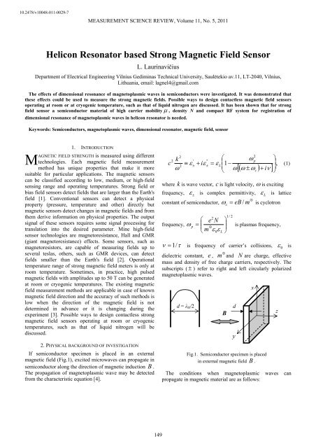
10.2478/v10048-011-0029-7<br />
MEASUREMENT SCIENCE REVIEW, Volume 11, No. 5, 2011<br />
<strong>Helicon</strong> <strong>Resonator</strong> <strong>based</strong> <strong>Strong</strong> <strong>Magnetic</strong> <strong>Field</strong> <strong>Sensor</strong><br />
L. Laurinavičius<br />
Department of Electrical Engineering Vilnius Gediminas Technical University, Saulėtekio av.11, LT-2040, Vilnius,<br />
Lithuania, email: lagnel4@gmail.com<br />
The effects of dimensional resonance of magnetoplasmic waves in semiconductors were investigated. It was demonstrated that<br />
these effects could be used to measure the strong magnetic fields. Possible ways to design contactless magnetic field sensors<br />
operating at room or at cryogenic temperature, such as that of liquid nitrogen are discussed. It has been shown that for strong<br />
field sensor a semiconductor material of high carrier mobility μ , density N and compact RF system for registration of<br />
dimensional resonance of magnetoplasmic waves in helicon resonator is needed.<br />
Keywords: Semiconductors, magnetoplasmic waves, dimensional resonator, magnetic field, sensor<br />
M<br />
1. INTRODUCTION<br />
AGNETIC FIELD STRENGTH is measured using different<br />
technologies. Each magnetic field measurement<br />
method has unique properties that make it more<br />
suitable for particular applications. The magnetic sensors<br />
can be classified according to low, medium, or high-field<br />
sensing range and operating temperatures. <strong>Strong</strong> field or<br />
bias field sensors detect fields that are larger than the Earth's<br />
field [1]. Conventional sensors can detect a physical<br />
property (pressure, temperature and other) directly but<br />
magnetic sensors detect changes in magnetic fields and from<br />
them derive information on physical properties. The output<br />
signal of these sensors requires some signal processing for<br />
translation into the desired parameter. Mine high-field<br />
sensor technologies are magnetoresistance, Hall and GMR<br />
(giant magnetoresistance) effects. Some sensors, such as<br />
magnetoresistors, are capable of measuring fields up to<br />
several teslas, others, such as GMR devices, can detect<br />
fields smaller than the Earth's field [2]. Operational<br />
temperature range of strong magnetic field meters is only at<br />
room temperature. Sometimes, in practice, high pulsed<br />
magnetic fields with amplitudes up to 50 T can be generated<br />
at room or cryogenic temperatures. The existing magnetic<br />
field measurement methods are applicable in case of known<br />
magnetic field direction and the accuracy of such methods is<br />
low when the direction of the magnetic field is not<br />
determined in advance or it is changing during the<br />
experiment [3]. Possible ways to design contactless strong<br />
magnetic field sensors operating at room or cryogenic<br />
temperatures, such as that of liquid nitrogen will be<br />
discussed.<br />
2. PHYSICAL BACKGROUND OF INVESTIGATION<br />
If semiconductor specimen is placed in an external<br />
magnetic field (Fig.1), excited microwaves can propagate in<br />
semiconductor along the direction of magnetic induction B .<br />
The propagation of magnetoplasmic wave may be detected<br />
from the characteristic equation [4].<br />
c<br />
2<br />
k<br />
ω<br />
2<br />
' ''<br />
≡ ε +<br />
2 ±<br />
iε<br />
±<br />
⎛<br />
= ε ⎜<br />
⎝<br />
2<br />
1 −<br />
ω<br />
ω<br />
⎞<br />
⎟<br />
⎠<br />
p<br />
[( ω ± ω ) + iν<br />
] ⎟<br />
,<br />
L<br />
(1)<br />
where k is wave vector, c is light velocity, ω is exciting<br />
frequency, ε<br />
±<br />
is complex permittivity, ε L<br />
is lattice<br />
⊗<br />
constant of semiconductor, ω = eB m is cyclotron<br />
c<br />
/<br />
1/ 2<br />
2<br />
frequency, ω ⎛ e N ⎞<br />
= ⎜<br />
⎟<br />
p ⊗<br />
⎝ m ε<br />
0ε<br />
is plasmas frequency,<br />
L ⎠<br />
ν = 1/τ<br />
is frequency of carrier’s collisions, ε<br />
0<br />
is<br />
⊗<br />
dielectric constant, e , m and N are charge, effective<br />
mass and density of free charge carriers, respectively. The<br />
subscripts ( ± ) refer to right and left circularly polarized<br />
magnetoplasmic waves.<br />
d = λ H /2<br />
B<br />
Fig.1. Semiconductor specimen is placed<br />
in external magnetic field B .<br />
The conditions when magnetoplasmic waves can<br />
propagate in magnetic material are as follows:<br />
d<br />
y<br />
x<br />
c<br />
z<br />
149
MEASUREMENT SCIENCE REVIEW, Volume 11, No. 5, 2011<br />
ω ± ω c<br />
>> ν ; ω >> ω;<br />
c cτ<br />
≡ μB >>1,<br />
ω (2)<br />
where μ is mobility of free charge carriers (electrons).<br />
The helicon waves (left polarized, direction of circular<br />
polarization coincides with cyclotron rotation of free charge<br />
carriers) are only of interest for practical application (for<br />
measurement of the strong magnetic fields).<br />
The equations of real and imaginary parts of complex<br />
permittivity for helicon wave in the case of strong magnetic<br />
field μ B >> 1 looks as follows [5]:<br />
2<br />
⎛<br />
'<br />
ω ⎞ ⎛ ⎞<br />
= ⎜1<br />
⎟ =<br />
⎜1<br />
+<br />
⎟<br />
+<br />
p<br />
eN<br />
ε<br />
−<br />
ε<br />
L<br />
ε<br />
L<br />
, (3)<br />
⎝ ωωc<br />
⎠ ⎝ ε<br />
Lε<br />
0ωB<br />
⎠<br />
2<br />
''<br />
ε<br />
Lω pν<br />
eN<br />
ε<br />
−<br />
= = .<br />
(4)<br />
2<br />
2<br />
ωω ε ωB<br />
μ<br />
The length of helicon waves<br />
equation<br />
c<br />
0<br />
λ H<br />
is determined by<br />
1/ 2<br />
c 1 c<br />
/ 2<br />
⎛ε<br />
0ωB<br />
λ = =<br />
⎞<br />
H<br />
⎜ ⎟ . (5)<br />
ω '<br />
ε ω ⎝ eN ⎠<br />
−<br />
It means that it is possible to determine the density of free<br />
charge carriers N by observation of resonances of<br />
magnetoplasmic microwaves in magnetic materials [6].<br />
When mine (half – length) dimensional resonance is<br />
observed, the value of density N is determined by simple<br />
equation<br />
N<br />
A⋅<br />
B<br />
2<br />
d ⋅<br />
= (6)<br />
Where<br />
R<br />
d = λ H<br />
/ 2 , d is<br />
thickness of the specimen and A = const.<br />
Physical background of the operation of magnetic field<br />
sensor is <strong>based</strong> on the effect of the dimensional resonance of<br />
magnetoplasmic waves in known semiconductor plate (free<br />
charge carriers N and μ ) placed in the static magnetic<br />
field.<br />
f is resonance frequency ( )<br />
f R<br />
3. RESULTS<br />
The technical possibility to realize the magnetic field<br />
induction B sensor with the help of high frequency Hall<br />
effect in semiconductors was proposed by the author [7]. A<br />
current-carrying InSb semiconductor plate is kept in a<br />
magnetic field and has two electrodes. The Hall voltage<br />
increases with applied field to several teslas. The<br />
temperature dependence of the voltage is governed by the<br />
temperature dependence of the carrier mobility μ . Different<br />
semiconductor materials and different doping levels result in<br />
trade-offs between sensitivity and temperature dependence<br />
of sensor.<br />
,<br />
The main objective of the present paper is to show that it is<br />
possible to determine the magnetic induction B by<br />
observation of dimensional resonances of magnetoplasmic<br />
microwaves in small size semiconductors. In<br />
semiconductors the phase velocity of magnetoplasmic<br />
microwaves is 10 4 times less than the speed of light. Thus<br />
the dimensions of resonators (thickness of plane-parallel<br />
plates, Fig.1) for mine dimensional resonance are less than<br />
1mm in high frequency (HF) range (wavelength in the free<br />
space λ < 10 m).<br />
A semiconductor sample (helicon resonator) should be<br />
placed into DC magnetic field B and AC microwave field<br />
b. Then, by satisfying the conditions of helicon origination<br />
(2) we may obtain coupling of coils of a resonant character.<br />
A non-contacting high field sensor may be developed by<br />
applying two perpendicular micro-strip lines (coils) to a<br />
semiconductor layer (plate) of finite dimensionality.<br />
Fig.2 shows the principle construction of a helicon<br />
resonator <strong>based</strong> magnetic field sensor. Two inner conductors<br />
coming from the inlet and output port cross under an angle<br />
of 90 degrees are connected to the outer conductor at the<br />
other end. They are isolated from each other where they<br />
cross each other. A semiconductor disk – helicon resonator<br />
is situated between the inner and outer conductors. A HF<br />
current in inner conductor (1) generates a HF magnetic field<br />
in the semiconductor disk. When the constant magnetic field<br />
B = 0, the oscillating magnetic field has only one<br />
component (for example b x ) and there is no signal in the<br />
outlet of the sensor. If field B ≠ 0, the perpendicular b y<br />
component will appear and magnetoplasmic helicon waves<br />
will coupling lumped elements. The interaction between<br />
magnetic fields of the windings and the average field of the<br />
standing wave in semiconductor has resonant character.<br />
Outer conductor<br />
Semiconductor<br />
disk (helicon<br />
resonator)<br />
Inner conductors 1<br />
2<br />
Outer conductor<br />
Fig.2. Principle construction of helicon resonator <strong>based</strong><br />
magnetic field sensor.<br />
The magnetic induction B can be easily calculated from<br />
typical amplitude frequency response in Fig.3:<br />
B = 1.28⋅10<br />
−25<br />
N ⋅ f<br />
R<br />
⋅<br />
d<br />
2<br />
.<br />
(7)<br />
150
MEASUREMENT SCIENCE REVIEW, Volume 11, No. 5, 2011<br />
The rate of coupling between the perpendicular micro-strip<br />
lines depends on quality Q of the dimensional resonator and<br />
on the filling of micro-strip lines by semiconductor core. In<br />
Fig.3 it is a measure of magnitude of the output as a function<br />
of frequency, in comparison to the input, when filling of<br />
micro-strip lines is different (amplitude vs. frequency<br />
dependences 1-4). Comparison of amplitude frequency<br />
responses shows, that amplitude of peak (quality Q of the<br />
dimensional resonator) is lower for partly filling sensor<br />
(curve 4).<br />
U/U 0 ,<br />
Relative units<br />
0,5<br />
1<br />
2<br />
A magnetic field sensor (1) is put in a magnetic field<br />
generated by axial solenoids (2). Fast switching RF signal<br />
generator (3) is connected through a coaxial cable to<br />
exciting micro-strip line (coil) (4): inner conductor of<br />
coaxial cable is connected to inner conductor of sensor and<br />
outer conductor (metallic shield) is connected to outer<br />
conductor of sensor. The helicon wave is excited in local<br />
area of a semiconductor core. Propagating across<br />
semiconductor helicon waves is indicated by receiving<br />
micro-strip line (coil) (5), situated perpendicularly to the<br />
exciting line. A receiving signal is registered by recorder<br />
(6). The described magnetoplasmic magnetic field meter has<br />
also a high frequency detector (7), cryogenic system, signal<br />
analyser and system for controlling radio frequency output,<br />
which are not shown.<br />
3<br />
0,05<br />
4<br />
2<br />
1<br />
4<br />
2<br />
0,005<br />
f R<br />
0 50 100 150 f, MHz<br />
Fig.3. A typical amplitude frequency response. Here U 0 and U are<br />
voltages of generated and indicated (propagated through<br />
semiconductor plate) high frequency signals.<br />
3<br />
6<br />
3<br />
For the development of strong magnetic field sensors a<br />
semiconductor material of high carrier mobility μ and high<br />
density N of main free charge carriers is needed.<br />
The most suitable semiconductor material for the magnetic<br />
field sensor is narrow-gap Te-doped n-InSb, where the<br />
ω c<br />
τ = 1 condition may be achieved in the magnetic fields<br />
of 0.2 Tesla (at room or cryogenic temperature) and density<br />
of electrons more times exceeding density of holes. For<br />
sensors operating at room or liquid nitrogen temperatures<br />
the semiconductor alloy Cd x Hg 1-x Te with high temperatureindependent<br />
density of electrons (x = 0.1- 0.15) is suitable.<br />
There are some possibilities to observe the dimensional<br />
resonances of magnetoplasmic microwaves in the<br />
semiconductor layer and to determine the resonant<br />
frequency.<br />
Since the resonant frequency of the objects under test is<br />
mainly in the radio frequency (RF) range (50-1000 MHz)<br />
and small sensor dimensions are required, we have<br />
employed a RF system. The helicon waves are excited by<br />
transmitting antenna. The scattered fields are then received<br />
by the receiving antenna, which has the capability of<br />
recording waveforms with bandwidth up to 1 GHz. To<br />
extract the resonant frequencies from the waves it is<br />
necessary to employ various data processing methods.<br />
A simplified block diagram of high magnetic field meter is<br />
shown in Fig.4.<br />
7<br />
5<br />
5<br />
Fig.4. Block diagram of high magnetic field meter<br />
The operation of the offered high magnetic field sensor<br />
has been demonstrated by measurement of magnetic<br />
induction (flux density) of magnetic systems with rare earth<br />
permanent magnet material: disc shape SmCo 5 magnets<br />
(diameter 55 mm and thickness 20 mm; max. energy<br />
(BH) max. = 20 MGOe; axially magnetized). The sensor is<br />
held at fixed distance (5 mm) from the face of the magnet or<br />
in the middle of 10 mm gap between two “iron-circuit”<br />
magnets (Fig. 5). The space between the poles of a magnet is<br />
filled with wood or any other non-magnetic material with a<br />
hole in the middle. The sensor can be fixed at any place of<br />
the sensor location hole and can scan the gap and provide<br />
flux density measurements at different points.<br />
Results of measurements using different magnetic field<br />
measurement techniques are shown in Fig.5. The<br />
measurements were repeated several times.<br />
151
fR<br />
9<br />
7<br />
5<br />
3<br />
MEASUREMENT SCIENCE REVIEW, Volume 11, No. 5, 2011<br />
2R<br />
B,T<br />
0,6<br />
0,4<br />
0,2<br />
SmCo 5<br />
Hall<br />
sensor<br />
<strong>Helicon</strong><br />
sensor<br />
-3 -2 -1 0 1 2 3<br />
R, cm<br />
Fig.5. A comparison of the measured magnetic field strength on<br />
the active surfaces of rare earth neodymium (NdFeB) or (SmCo)<br />
disc-type permanent “open-circuit” and “iron-circuit” magnets<br />
using Hall (magnetic field strength meter FH 55) and helicon<br />
sensor.<br />
A comparison of the curves produced by the Hall<br />
technology sensor (magnetic field strength meter FH 55)<br />
and the helicon resonator <strong>based</strong> magnetic field sensor<br />
shows rather good agreement of measurements in the centre<br />
of magnet gap (R < + 2 cm). At the corners of disk magnets<br />
( R = + 2.5 cm ) results of measurement are different. The<br />
misalignment relates to the sensor dimensions. <strong>Magnetic</strong><br />
field strength meter FH 55 is equipped with Hall technology<br />
probe with small active area of 0.4 mm (magnetic induction<br />
range 3T; probe temperature correction 300 K). Active area<br />
of helicon resonator <strong>based</strong> sensor is several times higher<br />
(2.5 mm) than the magnet edge impact observed earlier.<br />
For the measurement of magnetic fields lower than 2T, the<br />
most suitable semiconductor material for the sensors is alloy<br />
Cd x Hg 1-x Te or Te-doped n-InSb of high carrier mobility and<br />
high mine carrier density N > 0.5·10 23 m -3 , together with the<br />
electron density far exceeding that of the holes.<br />
At cryogenic temperatures it is advisable to make helicon<br />
resonator from the anisotropic alloy Bi 1-x Sb x (x = 0.1). The<br />
mobility of electrons in this alloy is several times higher<br />
than in the mentioned semiconductors (Tab. 1).<br />
For the magnetic fields exceeding 20 T, practically all<br />
semiconductor materials of high carrier mobility ( μ > 0.1<br />
m 2 V -1 s -1 ) are suitable for sensors, because ω c<br />
τ > 2. Other<br />
materials should be studied for their magnetic sensitivity<br />
and thermal stability.<br />
At cryogenic and at room temperatures f R (B) dependence<br />
is linear (Fig.6, 7).<br />
Tab.1. Electrical and temperature parameters of semiconductor<br />
material for strong magnetic field sensor<br />
Semiconductor<br />
material<br />
Density<br />
N ,<br />
m -3<br />
Mobility<br />
μ ,<br />
m 2 V -1 s -1<br />
Temperature<br />
T, K<br />
n- InSb 2·10 23 3.5 300<br />
n- InSb 8·10 22 4.8 300<br />
n- InSb 1·10 23 6.5 77<br />
Cd x Hg 1-x Te<br />
(x=0.12)<br />
Bi 1-x Sb x<br />
(x=0.1)<br />
5·10 22 10 77<br />
2.5·10 23 30 77<br />
f R , MHz<br />
500<br />
d=0.5 mm<br />
N=1·10 23 m -3<br />
T=77 K<br />
300<br />
100<br />
0<br />
0.4 0.8 1.2 1.6 2.0 B, T<br />
Fig.6. Resonance frequency f R dependence from magnetic induction B at liquid nitrogen (T=77 K)<br />
temperature: calculation (dashed line); experiment (points).<br />
152
fR<br />
9<br />
7<br />
5<br />
3<br />
MEASUREMENT SCIENCE REVIEW, Volume 11, No. 5, 2011<br />
f R , MHz<br />
90<br />
70<br />
d=0.5 mm<br />
N=2·10 23 m -3<br />
T=300 K<br />
50<br />
30<br />
10<br />
0<br />
1.0 2.0 3.0 4.0 5.0 6.0 B, T<br />
Fig.7. Resonance frequency<br />
f<br />
R dependence from magnetic induction B at room (T=300 K) temperature:<br />
calculation (dashed line); experiment (points).<br />
4. CONCLUSION<br />
The measurements of magnetic induction with the help of<br />
helicon waves in semiconductors can be provided in<br />
contactless mode. Practically all semiconductor materials of<br />
high carrier mobility can be put into practice for<br />
measurement high magnetic field (~20 tesla).<br />
<strong>Magnetic</strong> field sensing with the help of semiconductor<br />
helicon resonator can be used at cryogenic temperatures as<br />
well. It was demonstrated that frequency dependence<br />
between the measurement of magnetic field induction and<br />
the main resonator is linear in a wide temperature range.<br />
Principle construction of helicon resonator <strong>based</strong> small size<br />
magnetic field sensor, using RF system was demonstrated.<br />
Comparison of results obtained from measurement<br />
permanent magnets using different techniques was done.<br />
REFERENCES<br />
[1] Lenz, J.E. (1990). A review of magnetic sensors.<br />
Proceedings of the IEEE, 78 (6), 973-989.<br />
[2] Michael, J.C., Bratland, T., Smith, C.H., Schneider, R.<br />
(1998). A new perspective on magnetic field sensing.<br />
<strong>Sensor</strong>s Magazine, 15 (12), 34-46.<br />
[3] Bartkevičius, S. et al. (2006). Data processing of<br />
manganite sensors array for measurements of nonhomogeneous<br />
pulsed magnetic field. Electronics and<br />
Electrical Engineering, 4 (68), 69-72.<br />
[4] Palik, E.D., Furdina, J.K. (1970). Infrared and<br />
microwave magnetoplasma effects in semiconductors.<br />
Report on Progress in Physics, 33, 1195-1322.<br />
[5] Jankauskas, Z., Laurinavicius, L. (2002). <strong>Magnetic</strong> and<br />
electric excitation of magnetoplasmic waves.<br />
Electronics and Electrical Engineering, 2 (37), 32-34.<br />
[6] Jankauskas, Z., Kvedaras, V., Laurinavicius, L. (2003).<br />
The measurements of carrier density and mobility in<br />
magnetised materials by the help of helicon maser.<br />
Measurement Science Review, 3 (3), 123-126.<br />
[7] Laurinavičius, L. et al. (1990). <strong>Strong</strong> <strong>Magnetic</strong> <strong>Field</strong><br />
<strong>Sensor</strong>. U.S.S.R. Patent 1,584,676 A1.<br />
Received June 13, 2011.<br />
Accepted October 21, 2011.<br />
153