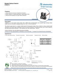
Silicon Phototransistor - OPTEK Technology
Silicon Phototransistor - OPTEK Technology
Silicon Phototransistor - OPTEK Technology

Create successful ePaper yourself
Turn your PDF publications into a flip-book with our unique Google optimized e-Paper software.
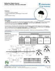
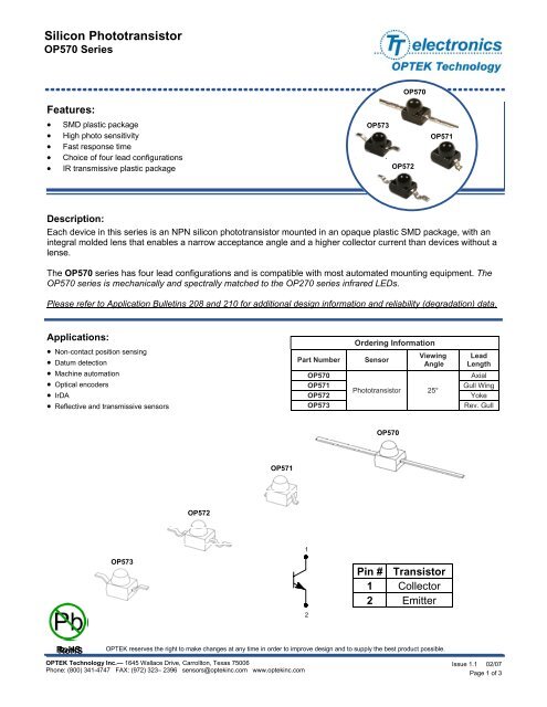
<strong>Silicon</strong> <strong>Phototransistor</strong><br />
OP570 Series<br />
Features:<br />
• SMD plastic package<br />
• High photo sensitivity<br />
• Fast response time<br />
• Choice of four lead configurations<br />
• IR transmissive plastic package<br />
OP573<br />
OP572<br />
OP570<br />
OP571<br />
Description:<br />
Each device in this series is an NPN silicon phototransistor mounted in an opaque plastic SMD package, with an<br />
integral molded lens that enables a narrow acceptance angle and a higher collector current than devices without a<br />
lense.<br />
The OP570 series has four lead configurations and is compatible with most automated mounting equipment. The<br />
OP570 series is mechanically and spectrally matched to the OP270 series infrared LEDs.<br />
Please refer to Application Bulletins 208 and 210 for additional design information and reliability (degradation) data.<br />
Applications:<br />
• Non-contact position sensing<br />
• Datum detection<br />
• Machine automation<br />
• Optical encoders<br />
• IrDA<br />
• Reflective and transmissive sensors<br />
Part Number<br />
OP570<br />
OP571<br />
OP572<br />
OP573<br />
Ordering Information<br />
Sensor<br />
Viewing<br />
Angle<br />
<strong>Phototransistor</strong> 25°<br />
Lead<br />
Length<br />
Axial<br />
Gull Wing<br />
Yoke<br />
Rev. Gull<br />
OP570<br />
OP571<br />
OP571<br />
OP572<br />
OP573<br />
1<br />
2<br />
Pin # Transistor<br />
1 Collector<br />
2 Emitter<br />
RoHS<br />
<strong>OPTEK</strong> reserves the right to make changes at any time in order to improve design and to supply the best product possible.<br />
<strong>OPTEK</strong> <strong>Technology</strong> Inc.— 1645 Wallace Drive, Carrollton, Texas 75006<br />
Phone: (800) 341-4747 FAX: (972) 323– 2396 sensors@optekinc.com www.optekinc.com<br />
Issue 1.1 02/07<br />
Page 1 of 3
<strong>Silicon</strong> <strong>Phototransistor</strong><br />
OP570 Series<br />
OP573<br />
DIMENSIONS ARE IN:<br />
[MILLIMETERS]<br />
INCHES<br />
OP570<br />
TOLERANCE IS ± .0039 [0.1]<br />
OP571<br />
OP572<br />
2<br />
1<br />
Pin # Transistor<br />
1 Collector<br />
2 Emitter<br />
<strong>OPTEK</strong> reserves the right to make changes at any time in order to improve design and to supply the best product possible.<br />
Issue 1.2 02/07<br />
Page 2 of 4<br />
<strong>OPTEK</strong> <strong>Technology</strong> Inc. — 1645 Wallace Drive, Carrollton, Texas 75006<br />
Phone: (972) 323-2200 or (800) 341-4747 FAX: (972) 323-2396 sensors@optekinc.com www.optekinc.com
<strong>Silicon</strong> <strong>Phototransistor</strong><br />
OP570 Series<br />
Absolute Maximum Ratings (T A =25°C unless otherwise noted)<br />
Storage Temperature Range<br />
Operating Temperature Range<br />
Collector-Emitter Voltage<br />
Emitter-Collector Voltage<br />
Collector Current<br />
-40 o C to +85 o C<br />
-25 o C to +85 o C<br />
30 V<br />
Lead Soldering Temperature [1/16 inch (1.6 mm) from case for 5 seconds with soldering iron] 260° C (1)<br />
Power Dissipation 130 mW (2)<br />
Notes:<br />
1. Solder time less than 5 seconds at temperature extreme.<br />
2. Derate linearly at 2.17 mW/° C above 25° C.<br />
Electrical Characteristics (T A = 25°C unless otherwise noted)<br />
SYMBOL PARAMETER MIN TYP MAX UNITS TEST CONDITIONS<br />
Input Diode<br />
I C (ON) On-State Collector Current 2.5 - - mA V CE = 5.0 V, E E = 5.0 mW/cm 2 (1)<br />
V CE(SAT) Forward Voltage - - 0.4 V I C = 100 µA, E E = 2.0 mW/cm 2 (1)<br />
I CEO Reverse Current - - 100 nA V CE = 5.0 V, E E = 0 (2)<br />
V BR(CEO) Wavelength at Peak Emission 30 - - V I C = 100 µA<br />
V (BR)ECO Emission Angle at Half Power Points 5 - - V I E = 100 µA<br />
Notes:<br />
1. Light source is an unfiltered GaAl LED with a peak emission wavelength of 935nm and a radiometric intensity level which varies less<br />
than 10% over the entire lens surface of the phototransistor being tested.<br />
2. To calculate typical collector dark current in µA, use the formula I CEO = 10 (0.04 Ta-3.4) where Ta is the ambient temperature in ° C.<br />
5 V<br />
20 mA<br />
Relative Collector Current<br />
160%<br />
140%<br />
120%<br />
100%<br />
80%<br />
60%<br />
40%<br />
20%<br />
Relative On-State Collector<br />
Current vs. Irradiance<br />
Normalized at Ee = 5mW/cm 2<br />
Conditions: VCE = 5V,<br />
λ = 935nm, TA = 25 °C<br />
Relative Collector Current<br />
140%<br />
130%<br />
120%<br />
110%<br />
100%<br />
90%<br />
80%<br />
70%<br />
Relative On-State Collector Current<br />
vs. Temperature<br />
Normalized at TA = 25°C .<br />
Conditions: VCE = 5V,<br />
λ = 935nm, TA = 25 °C<br />
0 1.0 2.0 3.0 4.0<br />
Ee—Irradiance (mW/cm 2 )<br />
5.0 6.0 7.0 8.0<br />
-25 0 25 50 75 100<br />
Temperature—(°C)<br />
<strong>OPTEK</strong> reserves the right to make changes at any time in order to improve design and to supply the best product possible.<br />
<strong>OPTEK</strong> <strong>Technology</strong> Inc. — 1645 Wallace Drive, Carrollton, Texas 75006<br />
Phone: (972) 323-2200 or (800) 341-4747 FAX: (972) 323-2396 sensors@optekinc.com www.optekinc.com<br />
Issue 1.2 02/07<br />
Page 3 of 4
<strong>Silicon</strong> <strong>Phototransistor</strong><br />
OP570 Series<br />
Relative Response<br />
100%<br />
80%<br />
60%<br />
40%<br />
20%<br />
Relative Response vs.<br />
Angular Position<br />
0%<br />
-90 -60 -30 0 30 60 90<br />
Angular Position (Degrees)<br />
IC(ON) - On-State Collector Current (mA)<br />
2.00<br />
1.80<br />
1.60<br />
1.40<br />
1.20<br />
1.00<br />
0.80<br />
0.60<br />
0.40<br />
0.20<br />
Relative On-State Collector Current<br />
vs. Collector-Emitter Voltage<br />
6 mW/cm 2<br />
5 mW/cm 2<br />
4 mW/cm 2<br />
3 mW/cm 2<br />
2 mW/cm 2<br />
1 mW/cm 2<br />
0 0.1 0.2 0.3 0.4 0.5<br />
Collector-Emitter Voltage (V)<br />
1000<br />
Collector-Emitter Dark Current<br />
vs. Temperature<br />
Conditions: Ee = 0 mW/cm 2<br />
VCE = 10V<br />
100%<br />
Relative Response vs. Wavelength<br />
Collector-Emitter Dark Current (nA)<br />
100<br />
10<br />
1<br />
Relative Response<br />
80%<br />
60%<br />
40%<br />
20%<br />
0<br />
-25 0 25 50 75 100<br />
Temperature—(°C)<br />
0%<br />
400<br />
500<br />
600<br />
700<br />
800<br />
Wavelength (nm)<br />
900 1000 1100<br />
<strong>OPTEK</strong> reserves the right to make changes at any time in order to improve design and to supply the best product possible.<br />
Issue 1.2 02/07<br />
Page 4 of 4<br />
<strong>OPTEK</strong> <strong>Technology</strong> Inc. — 1645 Wallace Drive, Carrollton, Texas 75006<br />
Phone: (972) 323-2200 or (800) 341-4747 FAX: (972) 323-2396 sensors@optekinc.com www.optekinc.com