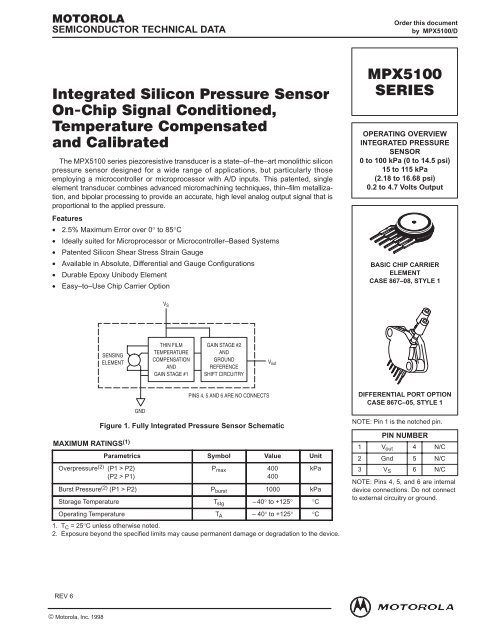
Integrated Silicon Pressure Sensor On-Chip Signal Conditioned ...
Integrated Silicon Pressure Sensor On-Chip Signal Conditioned ...
Integrated Silicon Pressure Sensor On-Chip Signal Conditioned ...

You also want an ePaper? Increase the reach of your titles
YUMPU automatically turns print PDFs into web optimized ePapers that Google loves.
SEMICONDUCTOR TECHNICAL DATA<br />
Order this document<br />
by MPX5100/D<br />
<br />
<br />
<br />
<br />
The MPX5100 series piezoresistive transducer is a state–of–the–art monolithic silicon<br />
pressure sensor designed for a wide range of applications, but particularly those<br />
employing a microcontroller or microprocessor with A/D inputs. This patented, single<br />
element transducer combines advanced micromachining techniques, thin–film metallization,<br />
and bipolar processing to provide an accurate, high level analog output signal that is<br />
proportional to the applied pressure.<br />
Features<br />
• 2.5% Maximum Error over 0° to 85°C<br />
• Ideally suited for Microprocessor or Microcontroller–Based Systems<br />
• Patented <strong>Silicon</strong> Shear Stress Strain Gauge<br />
• Available in Absolute, Differential and Gauge Configurations<br />
• Durable Epoxy Unibody Element<br />
• Easy–to–Use <strong>Chip</strong> Carrier Option<br />
<br />
<br />
OPERATING OVERVIEW<br />
INTEGRATED PRESSURE<br />
SENSOR<br />
0 to 100 kPa (0 to 14.5 psi)<br />
15 to 115 kPa<br />
(2.18 to 16.68 psi)<br />
0.2 to 4.7 Volts Output<br />
BASIC CHIP CARRIER<br />
ELEMENT<br />
CASE 867–08, STYLE 1<br />
V S<br />
SENSING<br />
ELEMENT<br />
THIN FILM<br />
TEMPERATURE<br />
COMPENSATION<br />
AND<br />
GAIN STAGE #1<br />
GAIN STAGE #2<br />
AND<br />
GROUND<br />
REFERENCE<br />
SHIFT CIRCUITRY<br />
V out<br />
MAXIMUM RATINGS (1)<br />
Overpressure (2) (P1 > P2)<br />
(P2 > P1)<br />
GND<br />
PINS 4, 5 AND 6 ARE NO CONNECTS<br />
Figure 1. Fully <strong>Integrated</strong> <strong>Pressure</strong> <strong>Sensor</strong> Schematic<br />
Parametrics Symbol Value Unit<br />
P max 400<br />
400<br />
Burst <strong>Pressure</strong> (2) (P1 > P2) P burst 1000 kPa<br />
Storage Temperature T stg –40° to +125° °C<br />
Operating Temperature T A –40° to +125° °C<br />
1. T C = 25°C unless otherwise noted.<br />
2. Exposure beyond the specified limits may cause permanent damage or degradation to the device.<br />
kPa<br />
DIFFERENTIAL PORT OPTION<br />
CASE 867C–05, STYLE 1<br />
NOTE: Pin 1 is the notched pin.<br />
1<br />
2<br />
3<br />
PIN NUMBER<br />
V out 4<br />
Gnd 5<br />
V S 6<br />
N/C<br />
N/C<br />
N/C<br />
NOTE: Pins 4, 5, and 6 are internal<br />
device connections. Do not connect<br />
to external circuitry or ground.<br />
REV 6<br />
Motorola <strong>Sensor</strong> Device Data<br />
© Motorola, Inc. 1998<br />
1
P 0<br />
OPERATING CHARACTERISTICS (V S = 5.0 Vdc, T A = 25°C unless otherwise noted, P1 > P2)<br />
Characteristic Symbol Min Typ Max Unit<br />
<strong>Pressure</strong> Range (1) Gauge, Differential: MPX5100D<br />
—<br />
100<br />
kPa<br />
Vacuum: MPX5100GV (11) 0<br />
—<br />
100<br />
Absolute: MPX5100A<br />
OP<br />
15<br />
—<br />
115<br />
Supply Voltage (2) V S 4.75 5.0 5.25 Vdc<br />
Supply Current I o — 7.0 10 mAdc<br />
Minimum <strong>Pressure</strong> Offset (3)<br />
@ V S = 5.0 Volts<br />
(0 to 85°C)<br />
V off 0.088 0.20 0.313 Vdc<br />
Full Scale Output (4) Differential and Absolute (0 to 85°C) V FSO 4.587<br />
@ V S = 5.0 Volts Vacuum (11) 3.688<br />
4.700<br />
3.800<br />
4.813<br />
3.913<br />
Vdc<br />
Full Scale Span (5) Differential and Absolute (0 to 85°C) V FSS —<br />
@ V S = 5.0 Volts Vacuum (11) —<br />
4.500<br />
3.600<br />
—<br />
—<br />
Vdc<br />
Accuracy (6) — — — 2.5 %V FSS<br />
Sensitivity V/P — 45 — mV/kPa<br />
Response Time (7) t R — 1.0 — mS<br />
Output Source Current at Full Scale Output I o+ — 0.1 — mAdc<br />
Warm–Up Time (8) — — 20 — mSec<br />
Offset Stability (9) — — 0.5 — %V FSS<br />
Decoupling circuit shown in Figure 4 required to meet electrical specifications.<br />
MECHANICAL CHARACTERISTICS<br />
Characteristic Symbol Min Typ Max Unit<br />
Weight, Basic Element (Case 867) — — 4.0 — Grams<br />
Common Mode Line <strong>Pressure</strong> (10) — — — 690 kPa<br />
NOTES:<br />
1. 1.0kPa (kiloPascal) equals 0.145 psi.<br />
2. Device is ratiometric within this specified excitation range.<br />
3. Offset (V off ) is defined as the output voltage at the minimum rated pressure.<br />
4. Full Scale Output (V FSO ) is defined as the output voltage at the maximum or full rated pressure.<br />
5. Full Scale Span (V FSS ) is defined as the algebraic difference between the output voltage at full rated pressure and the output voltage at the<br />
minimum rated pressure.<br />
6. Accuracy (error budget) consists of the following:<br />
• Linearity: Output deviation from a straight line relationship with pressure over the specified pressure range.<br />
• Temperature Hysteresis: Output deviation at any temperature within the operating temperature range, after the temperature is<br />
cycled to and from the minimum or maximum operating temperature points, with zero differential pressure<br />
applied.<br />
• <strong>Pressure</strong> Hysteresis: Output deviation at any pressure within the specified range, when this pressure is cycled to and from<br />
minimum or maximum rated pressure at 25°C.<br />
• TcSpan: Output deviation over the temperature range of 0° to 85°C, relative to 25°C.<br />
• TcOffset: Output deviation with minimum pressure applied, over the temperature range of 0° to 85°C, relative<br />
to 25°C.<br />
• Variation from Nominal: The variation from nominal values, for Offset or Full Scale Span, as a percent of V FSS at 25°C.<br />
7. Response Time is defined as the time for the incremental change in the output to go from 10% to 90% of its final value when subjected to<br />
a specified step change in pressure.<br />
8. Warm–up is defined as the time required for the product to meet the specified output voltage after the <strong>Pressure</strong> has been stabilized.<br />
9. Offset stability is the product’s output deviation when subjected to 1000 hours of Pulsed <strong>Pressure</strong>, Temperature Cycling with Bias Test.<br />
10. Common mode pressures beyond what is specified may result in leakage at the case–to–lead interface.<br />
11. <strong>Pressure</strong> Range: Vacuum sensor is rated to 100 kPa; part is tested to a vacuum pressure equivalent to 80 kPa.<br />
2 Motorola <strong>Sensor</strong> Device Data
ÉÉÉÉÉÉÉÉÉÉÉÉ<br />
ÉÉÉÉÉÉÉÉÉÉÉÉ<br />
ÉÉÉÉÉÉÉÉÉÉÉ<br />
ÉÉÉÉÉÉÉÉÉÉÉ<br />
<br />
ON–CHIP TEMPERATURE COMPENSATION, CALIBRATION and SIGNAL CONDITIONING<br />
Figure 2 shows the sensor output signal relative to<br />
pressure input. Typical, minimum, and maximum output<br />
curves are shown for operation over a temperature<br />
range of 0° to 85°C using the decoupling circuit below.<br />
(The output will saturate outside of the specified pressure<br />
range.)<br />
OUTPUT (V)<br />
5<br />
4.5<br />
4<br />
3.5<br />
3<br />
2.5<br />
2<br />
1.5<br />
1<br />
0.5<br />
0<br />
0<br />
V S = 5 Vdc<br />
T A = 25°C<br />
MPX5100<br />
10<br />
20<br />
30<br />
40<br />
50<br />
TYP<br />
60<br />
MAX<br />
PRESSURE (kPa)<br />
70<br />
MIN<br />
80<br />
90<br />
100<br />
Figure 2. Output versus <strong>Pressure</strong> Differential<br />
110<br />
SPAN RANGE (TYP)<br />
OUTPUT RANGE (TYP)<br />
OFFSET<br />
(TYP)<br />
WIRE BOND<br />
FLUORO SILICONE<br />
GEL DIE COAT<br />
DIE<br />
STAINLESS STEEL<br />
METAL COVER<br />
EPOXY PLASTIC<br />
CASE<br />
WIRE BOND<br />
FLUORO SILICONE<br />
GEL DIE COAT<br />
DIE<br />
STAINLESS STEEL<br />
METAL COVER<br />
EPOXY PLASTIC<br />
CASE<br />
LEAD FRAME<br />
DIE<br />
BOND<br />
ÉÉÉÉÉÉÉÉÉÉÉÉ<br />
DIFFERENTIAL/GAUGE ELEMENT<br />
LEAD FRAME<br />
ÉÉÉÉÉÉÉÉÉÉÉ<br />
ABSOLUTE ELEMENT<br />
DIE<br />
BOND<br />
ÉÉÉÉÉÉÉÉÉÉÉÉ<br />
ÉÉÉÉÉÉÉÉÉÉÉ<br />
ÉÉÉÉÉÉÉÉÉÉÉÉ<br />
ÉÉÉÉÉÉÉÉÉÉÉ<br />
Figure 3. Cross–Sectional Diagrams<br />
(Not to Scale)<br />
Figure 3 illustrates both the Differential/Gauge and the<br />
Absolute Sensing <strong>Chip</strong> in the basic chip carrier (Case 867). A<br />
fluorosilicone gel isolates the die surface and wire bonds<br />
from the environment, while allowing the pressure signal to<br />
be transmitted to the sensor diaphragm.<br />
The MPX5100 series pressure sensor operating characteristics,<br />
and internal reliability and qualification tests<br />
are based on use of dry air as the pressure media. Media,<br />
other than dry air, may have adverse effects on sensor<br />
performance and long–term reliability. Contact the factory<br />
for information regarding media compatibility in your<br />
application.<br />
5 V<br />
V S<br />
V out<br />
OUTPUT<br />
1.0 F<br />
0.01 F<br />
IPS<br />
GND<br />
Figure 4. Recommended Power Supply Decoupling.<br />
For output filtering recommendations, please refer to<br />
Application Note AN1646.<br />
Motorola <strong>Sensor</strong> Device Data<br />
3
Transfer Function (MPX5100D, MPX5100GV)<br />
Nominal Transfer Value: V out = V S (P x 0.009 + 0.04)<br />
+/– (<strong>Pressure</strong> Error x Temp. Mult. x 0.009 x V S )<br />
V S = 5.0 V ±5% P kPa<br />
Temperature Error Multiplier<br />
Break MPX5100D Points Series<br />
4.0<br />
3.0<br />
Temp<br />
Multiplier<br />
– 40 3<br />
0 to 85 1<br />
+125 3<br />
2.0<br />
1.0<br />
0.0<br />
–40 –20 0 20 40 60 80 100 120 130<br />
Temperature in °C<br />
140<br />
NOTE: The Temperature Multiplier is a linear response from 0° to –40°C and from 85° to 125°C.<br />
<strong>Pressure</strong> Error Band<br />
3.0<br />
Error Limits for <strong>Pressure</strong><br />
2.0<br />
Error (kPa)<br />
1.0<br />
0.0<br />
–1.0<br />
0 20 40 60 80 100 120<br />
<strong>Pressure</strong> in kPa<br />
–2.0<br />
MPX5100D Series<br />
–3.0<br />
<strong>Pressure</strong><br />
Error (max)<br />
0 to 100 kPa ± 2.5 kPa<br />
NOTE: For vacuum type parts (5100GV), Transfer Function is the same as that for 5100D Series.<br />
4 Motorola <strong>Sensor</strong> Device Data
Transfer Function (MPX5100A)<br />
<br />
Nominal Transfer Value: V out = V S (P x 0.009 – 0.095)<br />
+/– (<strong>Pressure</strong> Error x Temp. Mult. x 0.009 x V S )<br />
V S = 5.0 V ±5% P kPa<br />
Temperature Error Multiplier<br />
Break MPX5100A Points Series<br />
4.0<br />
3.0<br />
Temp<br />
Multiplier<br />
– 40 3<br />
0 to 85 1<br />
+125 3<br />
2.0<br />
1.0<br />
0.0<br />
–40 –20 0 20 40 60 80 100 120 130<br />
Temperature in °C<br />
140<br />
NOTE: The Temperature Multiplier is a linear response from 0° to –40°C and from 85° to 125°C.<br />
<strong>Pressure</strong> Error Band<br />
3.0<br />
Error Limits for <strong>Pressure</strong><br />
2.0<br />
Error (kPa)<br />
1.0<br />
0.0<br />
–1.0<br />
0 20 40 60 80 100 130<br />
<strong>Pressure</strong> in kPa<br />
–2.0<br />
MPX5100A Series<br />
–3.0<br />
<strong>Pressure</strong><br />
Error (max)<br />
15 to 115 kPa ± 2.5 kPa<br />
Motorola <strong>Sensor</strong> Device Data<br />
5
PRESSURE (P1)/VACUUM (P2) SIDE IDENTIFICATION TABLE<br />
Motorola designates the two sides of the pressure sensor<br />
as the <strong>Pressure</strong> (P1) side and the Vacuum (P2) side. The<br />
<strong>Pressure</strong> (P1) side is the side containing fluoro silicone gel<br />
which protects the die from harsh media. The Motorola MPX<br />
pressure sensor is designed to operate with positive differential<br />
pressure applied, P1 > P2.<br />
The <strong>Pressure</strong> (P1) side may be identified by using the<br />
Table below:<br />
Part Number<br />
Case Type<br />
<strong>Pressure</strong> (P1)<br />
Side Identifier<br />
MPX5100A, MPX5100D 867–08 Stainless Steel Cap<br />
MPX5100DP 867C–05 Side with Part Marking<br />
MPX5100AP, MPX5100GP 867B–04 Side with Port Attached<br />
MPX5100GVP 867D–04 Stainless Steel Cap<br />
MPX5100AS, MPX5100GS 867E–03 Side with Port Attached<br />
MPX5100GVS 867A–04 Stainless Steel Cap<br />
MPX5100ASX, MPX5100GSX 867F–03 Side with Port Attached<br />
MPX5100GVSX 867G–03 Stainless Steel Cap<br />
ORDERING INFORMATION:<br />
The MPX5100 pressure sensor is available in absolute, differential, and gauge configurations. Devices are available in the<br />
basic element package or with pressure port fittings that provide printed circuit board mounting ease and barbed hose pressure<br />
connections.<br />
MPX Series<br />
Device Name Options Case Type Order Number Device Marking<br />
Basic Element Absolute 867–08 MPX5100A MPX5100A<br />
Differential 867–08 MPX5100D MPX5100D<br />
Ported Elements Differential Dual Ports 867C–05 MPX5100DP MPX5100DP<br />
Absolute, Single Port 867B–04 MPX5100AP MPX5100AP<br />
Gauge, Single Port 867B–04 MPX5100GP MPX5100GP<br />
Gauge, Vacuum Port 867D–04 MPX5100GVP MPX5100GVP<br />
Absolute, Axial 867E–03 MPX5100AS MPX5100A<br />
Gauge, Axial 867E–03 MPX5100GS MPX5100D<br />
Gauge, Vacuum Axial 867A–04 MPX5100GVS MPX5100D<br />
Absolute, Axial PC Mount 867F–03 MPX5100ASX MPX5100A<br />
Gauge, Axial PC Mount 867F–03 MPX5100GSX MPX5100D<br />
Gauge Vacuum Axial PC Mount 867G–03 MPX5100GVSX MPX5100D<br />
6 Motorola <strong>Sensor</strong> Device Data
PACKAGE DIMENSIONS<br />
B<br />
J<br />
S<br />
C<br />
M<br />
–A–<br />
SEATING<br />
PLANE<br />
PIN 1<br />
–T–<br />
F<br />
R<br />
1 2 3 4 5 6<br />
D 6 PL<br />
G<br />
N<br />
POSITIVE PRESSURE<br />
(P1)<br />
L<br />
0.136 (0.005) M T<br />
A<br />
M<br />
NOTES:<br />
1. DIMENSIONING AND TOLERANCING PER ANSI<br />
Y14.5M, 1982.<br />
2. CONTROLLING DIMENSION: INCH.<br />
3. DIMENSION –A– IS INCLUSIVE OF THE MOLD<br />
STOP RING. MOLD STOP RING NOT TO EXCEED<br />
16.00 (0.630).<br />
INCHES MILLIMETERS<br />
DIM MIN MAX MIN MAX<br />
A 0.595 0.630 15.11 16.00<br />
B 0.514 0.534 13.06 13.56<br />
C 0.200 0.220 5.08 5.59<br />
D 0.027 0.033 0.68 0.84<br />
F 0.048 0.064 1.22 1.63<br />
G 0.100 BSC 2.54 BSC<br />
J 0.014 0.016 0.36 0.40<br />
L 0.695 0.725 17.65 18.42<br />
M 30 NOM 30 NOM<br />
N 0.475 0.495 12.07 12.57<br />
R 0.430 0.450 10.92 11.43<br />
S 0.090 0.105 2.29 2.66<br />
CASE 867–08<br />
ISSUE N<br />
STYLE 1:<br />
PIN 1. VOUT<br />
2. GROUND<br />
3. VCC<br />
4. V1<br />
5. V2<br />
6. VEX<br />
BASIC ELEMENT (A, D)<br />
C<br />
A<br />
–B– V<br />
PORT #2<br />
VACUUM<br />
(P2)<br />
N<br />
E<br />
–T–<br />
POSITIVE<br />
PRESSURE<br />
(P1)<br />
PIN 1<br />
K<br />
S<br />
J<br />
1 2 3 4 5 6<br />
G<br />
F<br />
CASE 867A–04<br />
ISSUE E<br />
D 6 PL<br />
0.13 (0.005) M T<br />
B<br />
M<br />
NOTES:<br />
1. DIMENSIONING AND TOLERANCING PER ANSI<br />
Y14.5M, 1982.<br />
2. CONTROLLING DIMENSION: INCH.<br />
INCHES MILLIMETERS<br />
DIM MIN MAX MIN MAX<br />
A 0.690 0.720 17.53 18.28<br />
B 0.245 0.255 6.22 6.48<br />
C 0.780 0.820 19.81 20.82<br />
D 0.027 0.033 0.69 0.84<br />
E 0.178 0.186 4.52 4.72<br />
F 0.048 0.064 1.22 1.63<br />
G 0.100 BSC 2.54 BSC<br />
J 0.014 0.016 0.36 0.41<br />
K 0.345 0.375 8.76 9.53<br />
N 0.300 0.310 7.62 7.87<br />
S 0.220 0.240 5.59 6.10<br />
V 0.182 0.194 4.62 4.93<br />
STYLE 1:<br />
PIN 1. VOUT<br />
2. GROUND<br />
3. VCC<br />
4. V1<br />
5. V2<br />
6. VEX<br />
VACUUM SIDE PORTED (GVS)<br />
Motorola <strong>Sensor</strong> Device Data<br />
7
PACKAGE DIMENSIONS–CONTINUED<br />
C<br />
J<br />
–T–<br />
R<br />
SEATING<br />
PLANE<br />
N<br />
B<br />
PIN 1<br />
–P–<br />
G<br />
0.25 (0.010) M T Q M<br />
F<br />
V<br />
A<br />
U<br />
L<br />
1 2 3 4 5 6<br />
D 6 PL<br />
CASE 867B–04<br />
ISSUE E<br />
PORT #1<br />
POSITIVE<br />
PRESSURE (P1)<br />
–Q–<br />
S<br />
K<br />
0.13 (0.005) M T P S Q S<br />
NOTES:<br />
1. DIMENSIONING AND TOLERANCING PER ANSI<br />
Y14.5M, 1982.<br />
2. CONTROLLING DIMENSION: INCH.<br />
INCHES MILLIMETERS<br />
DIM MIN MAX MIN MAX<br />
A 1.145 1.175 29.08 29.85<br />
B 0.685 0.715 17.40 18.16<br />
C 0.305 0.325 7.75 8.26<br />
D 0.027 0.033 0.68 0.84<br />
F 0.048 0.064 1.22 1.63<br />
G 0.100 BSC 2.54 BSC<br />
J 0.014 0.016 0.36 0.41<br />
K 0.695 0.725 17.65 18.42<br />
L 0.290 0.300 7.37 7.62<br />
N 0.420 0.440 10.67 11.18<br />
P 0.153 0.159 3.89 4.04<br />
Q 0.153 0.159 3.89 4.04<br />
R 0.230 0.250 5.84 6.35<br />
S 0.220 0.240 5.59 6.10<br />
U 0.910 BSC 23.11 BSC<br />
V 0.182 0.194 4.62 4.93<br />
STYLE 1:<br />
PIN 1. VOUT<br />
2. GROUND<br />
3. VCC<br />
4. V1<br />
5. V2<br />
6. VEX<br />
PRESSURE SIDE PORTED (AP, GP)<br />
PORT #1<br />
POSITIVE<br />
PRESSURE<br />
(P1)<br />
PORT #2<br />
VACUUM<br />
(P2)<br />
X<br />
SEATING<br />
PLANE –T– –T–<br />
J<br />
P<br />
0.25 (0.010) M T Q<br />
R<br />
C<br />
N<br />
B<br />
SEATING<br />
PLANE<br />
M<br />
PIN 1<br />
G<br />
1 2 3 4 5 6<br />
F<br />
–A–<br />
U<br />
W<br />
L<br />
V<br />
D 6 PL<br />
CASE 867C–05<br />
ISSUE F<br />
PORT #2 VACUUM (P2)<br />
PORT #1 POSITIVE<br />
PRESSURE (P1)<br />
–Q–<br />
S<br />
0.13 (0.005) M<br />
K<br />
A<br />
M<br />
NOTES:<br />
1. DIMENSIONING AND TOLERANCING PER ANSI<br />
Y14.5M, 1982.<br />
2. CONTROLLING DIMENSION: INCH.<br />
INCHES MILLIMETERS<br />
DIM MIN MAX MIN MAX<br />
A 1.145 1.175 29.08 29.85<br />
B 0.685 0.715 17.40 18.16<br />
C 0.405 0.435 10.29 11.05<br />
D 0.027 0.033 0.68 0.84<br />
F 0.048 0.064 1.22 1.63<br />
G 0.100 BSC 2.54 BSC<br />
J 0.014 0.016 0.36 0.41<br />
K 0.695 0.725 17.65 18.42<br />
L 0.290 0.300 7.37 7.62<br />
N 0.420 0.440 10.67 11.18<br />
P 0.153 0.159 3.89 4.04<br />
Q 0.153 0.159 3.89 4.04<br />
R 0.063 0.083 1.60 2.11<br />
S 0.220 0.240 5.59 6.10<br />
U 0.910 BSC 23.11 BSC<br />
V 0.182 0.194 4.62 4.93<br />
W 0.310 0.330 7.87 8.38<br />
X 0.248 0.278 6.30 7.06<br />
STYLE 1:<br />
PIN 1. VOUT<br />
2. GROUND<br />
3. VCC<br />
4. V1<br />
5. V2<br />
6. VEX<br />
PRESSURE AND VACUUM SIDES PORTED (DP)<br />
8 Motorola <strong>Sensor</strong> Device Data
PACKAGE DIMENSIONS–CONTINUED<br />
<br />
0.25 (0.010) M T<br />
R<br />
–T–<br />
J<br />
SEATING<br />
PLANE<br />
C<br />
N<br />
B<br />
–P–<br />
Q M<br />
PIN 1<br />
G<br />
1 2 3 4 5 6<br />
F<br />
A<br />
U<br />
L<br />
V<br />
D 6 PL<br />
CASE 867D–04<br />
ISSUE F<br />
PORT #2<br />
VACUUM (P2)<br />
POSITIVE PRESSURE (P1)<br />
–Q–<br />
S<br />
K<br />
0.13 (0.005) M T P S Q S<br />
NOTES:<br />
1. DIMENSIONING AND TOLERANCING PER ANSI<br />
Y14.5M, 1982.<br />
2. CONTROLLING DIMENSION: INCH.<br />
INCHES MILLIMETERS<br />
DIM MIN MAX MIN MAX<br />
A 1.145 1.175 29.08 29.85<br />
B 0.685 0.715 17.40 18.16<br />
C 0.305 0.325 7.75 8.26<br />
D 0.027 0.033 0.68 0.84<br />
F 0.048 0.064 1.22 1.63<br />
G 0.100 BSC 2.54 BSC<br />
J 0.014 0.016 0.36 0.41<br />
K 0.695 0.725 17.65 18.42<br />
L 0.290 0.300 7.37 7.62<br />
N 0.420 0.440 10.67 11.18<br />
P 0.153 0.159 3.89 4.04<br />
Q 0.153 0.159 3.89 4.04<br />
R 0.230 0.250 5.84 6.35<br />
S 0.220 0.240 5.59 6.10<br />
U 0.910 BSC 23.11 BSC<br />
V 0.182 0.194 4.62 4.93<br />
STYLE 1:<br />
PIN 1. VOUT<br />
2. GROUND<br />
3. VCC<br />
4. V1<br />
5. V2<br />
6. VEX<br />
VACUUM SIDE PORTED (GVP)<br />
C<br />
A<br />
NOTES:<br />
1. DIMENSIONING AND TOLERANCING PER ANSI<br />
Y14.5M, 1982.<br />
2. CONTROLLING DIMENSION: INCH.<br />
–B–<br />
V<br />
PORT #1<br />
POSITIVE<br />
PRESSURE<br />
(P1)<br />
N<br />
E<br />
–T–<br />
J<br />
K<br />
S<br />
G<br />
6 5 4 3 2 1<br />
F<br />
D 6 PL<br />
PIN 1<br />
0.13 (0.005) M T<br />
B<br />
M<br />
INCHES MILLIMETERS<br />
DIM MIN MAX MIN MAX<br />
A 0.690 0.720 17.53 18.28<br />
B 0.245 0.255 6.22 6.48<br />
C 0.780 0.820 19.81 20.82<br />
D 0.027 0.033 0.69 0.84<br />
E 0.178 0.186 4.52 4.72<br />
F 0.048 0.064 1.22 1.63<br />
G 0.100 BSC 2.54 BSC<br />
J 0.014 0.016 0.36 0.41<br />
K 0.345 0.375 8.76 9.53<br />
N 0.300 0.310 7.62 7.87<br />
S 0.220 0.240 5.59 6.10<br />
V 0.182 0.194 4.62 4.93<br />
STYLE 1:<br />
PIN 1. VOUT<br />
2. GROUND<br />
3. VCC<br />
4. V1<br />
5. V2<br />
6. VEX<br />
CASE 867E–03<br />
ISSUE D<br />
PRESSURE SIDE PORTED (AS, GS)<br />
Motorola <strong>Sensor</strong> Device Data<br />
9
PACKAGE DIMENSIONS–CONTINUED<br />
C<br />
E<br />
–T–<br />
A<br />
U<br />
–Q–<br />
NOTES:<br />
1. DIMENSIONING AND TOLERANCING PER<br />
ANSI Y14.5M, 1982.<br />
2. CONTROLLING DIMENSION: INCH.<br />
V<br />
PORT #1<br />
POSITIVE<br />
PRESSURE<br />
(P1)<br />
J<br />
–P–<br />
0.25 (0.010) M T<br />
D 6 PL<br />
0.13 (0.005) M T P S Q S<br />
Q<br />
M<br />
F<br />
6 5 4 3 2 1<br />
G<br />
K<br />
PIN 1<br />
N<br />
S<br />
R<br />
B<br />
INCHES MILLIMETERS<br />
DIM MIN MAX MIN MAX<br />
A 1.080 1.120 27.43 28.45<br />
B 0.740 0.760 18.80 19.30<br />
C 0.630 0.650 16.00 16.51<br />
D 0.027 0.033 0.68 0.84<br />
E 0.160 0.180 4.06 4.57<br />
F 0.048 0.064 1.22 1.63<br />
G 0.100 BSC 2.54 BSC<br />
J 0.014 0.016 0.36 0.41<br />
K 0.220 0.240 5.59 6.10<br />
N 0.070 0.080 1.78 2.03<br />
P 0.150 0.160 3.81 4.06<br />
Q 0.150 0.160 3.81 4.06<br />
R 0.440 0.460 11.18 11.68<br />
S 0.695 0.725 17.65 18.42<br />
U 0.840 0.860 21.34 21.84<br />
V 0.182 0.194 4.62 4.93<br />
STYLE 1:<br />
PIN 1. VOUT<br />
2. GROUND<br />
3. VCC<br />
4. V1<br />
5. V2<br />
6. VEX<br />
CASE 867F–03<br />
ISSUE D<br />
PRESSURE SIDE PORTED (ASX, GSX)<br />
V<br />
PORT #2<br />
VACUUM<br />
(P2)<br />
C<br />
J<br />
E<br />
–T–<br />
–P–<br />
POSITIVE<br />
PRESSURE<br />
(P1)<br />
PIN 1<br />
0.25 (0.010) M T<br />
D 6 PL<br />
0.13 (0.005) M T P S Q S<br />
Q<br />
M<br />
A<br />
U<br />
1 2 3 4 5 6<br />
F<br />
G<br />
K<br />
CASE 867G–03<br />
ISSUE D<br />
N<br />
S<br />
R<br />
–Q–<br />
B<br />
NOTES:<br />
1. DIMENSIONING AND TOLERANCING PER<br />
ANSI Y14.5M, 1982.<br />
2. CONTROLLING DIMENSION: INCH.<br />
INCHES MILLIMETERS<br />
DIM MIN MAX MIN MAX<br />
A 1.080 1.120 27.43 28.45<br />
B 0.740 0.760 18.80 19.30<br />
C 0.630 0.650 16.00 16.51<br />
D 0.027 0.033 0.68 0.84<br />
E 0.160 0.180 4.06 4.57<br />
F 0.048 0.064 1.22 1.63<br />
G 0.100 BSC 2.54 BSC<br />
J 0.014 0.016 0.36 0.41<br />
K 0.220 0.240 5.59 6.10<br />
N 0.070 0.080 1.78 2.03<br />
P 0.150 0.160 3.81 4.06<br />
Q 0.150 0.160 3.81 4.06<br />
R 0.440 0.460 11.18 11.68<br />
S 0.695 0.725 17.65 18.42<br />
U 0.840 0.860 21.34 21.84<br />
V 0.182 0.194 4.62 4.93<br />
STYLE 1:<br />
PIN 1. VOUT<br />
2. GROUND<br />
3. VCC<br />
4. V1<br />
5. V2<br />
6. VEX<br />
VACUUM SIDE PORTED (GVSX)<br />
10 Motorola <strong>Sensor</strong> Device Data
NOTES<br />
<br />
Motorola <strong>Sensor</strong> Device Data<br />
11
Mfax is a trademark of Motorola, Inc.<br />
Motorola reserves the right to make changes without further notice to any products herein. Motorola makes no warranty, representation or<br />
guarantee regarding the suitability of its products for any particular purpose, nor does Motorola assume any liability arising out of the application<br />
or use of any product or circuit, and specifically disclaims any and all liability, including without limitation consequential or incidental damages.<br />
“Typical” parameters which may be provided in Motorola data sheets and/or specifications can and do vary in different applications and actual<br />
performance may vary over time. All operating parameters, including “Typicals” must be validated for each customer application by customer’s<br />
technical experts. Motorola does not convey any license under its patent rights nor the rights of others. Motorola products are not designed,<br />
intended, or authorized for use as components in systems intended for surgical implant into the body, or other applications intended to support<br />
or sustain life, or for any other application in which the failure of the Motorola product could create a situation where personal injury or death<br />
may occur. Should Buyer purchase or use Motorola products for any such unintended or unauthorized application, Buyer shall indemnify and<br />
hold Motorola and its officers, employees, subsidiaries, affiliates, and distributors harmless against all claims, costs, damages, and expenses,<br />
and reasonable attorney fees arising out of, directly or indirectly, any claim of personal injury or death associated with such unintended or<br />
unauthorized use, even if such claim alleges that Motorola was negligent regarding the design or manufacture of the part. Motorola and<br />
are registered trademarks of Motorola, Inc. Motorola, Inc. is an Equal Opportunity/Affirmative Action Employer.<br />
How to reach us:<br />
USA/EUROPE/Locations Not Listed: Motorola Literature Distribution; P.O. Box 5405, Denver, Colorado 80217.<br />
1–303–675–2140 or 1–800–441–2447<br />
JAPAN: Motorola Japan Ltd.; SPS, Technical Information Center, 3–20–1, Minami–Azabu. Minato–ku, Tokyo 106–8573 Japan.<br />
81–3–3440–3569<br />
ASIA/PACIFIC: Motorola Semiconductors H.K. Ltd.; <strong>Silicon</strong> Harbour Centre, 2 Dai King Street, Tai Po Industrial Estate, Tai Po,<br />
N.T., Hong Kong. 852–26668334<br />
Customer Focus Center: 1–800–521–6274<br />
Mfax: RMFAX0@email.sps.mot.com – TOUCHTONE 1–602–244–6609<br />
Motorola Fax Back System – US & Canada ONLY 1–800–774–1848<br />
– http://sps.motorola.com/mfax/<br />
HOME PAGE: http://motorola.com/sps/<br />
12 Motorola <strong>Sensor</strong> Device Data<br />
◊<br />
MPX5100/D