Synchronous Sequential Logic The digital circuits considered thus ...
Synchronous Sequential Logic The digital circuits considered thus ...
Synchronous Sequential Logic The digital circuits considered thus ...
Create successful ePaper yourself
Turn your PDF publications into a flip-book with our unique Google optimized e-Paper software.
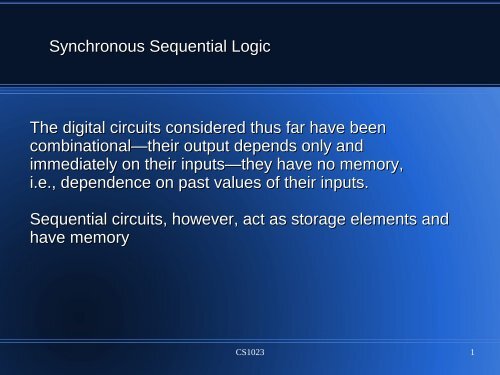
<strong>Synchronous</strong> <strong>Sequential</strong> <strong>Logic</strong><br />
<strong>The</strong> <strong>digital</strong> <strong>circuits</strong> <strong>considered</strong> <strong>thus</strong> far have been<br />
combinational—their output depends only and<br />
immediately on their inputs—they have no memory,<br />
i.e., dependence on past values of their inputs.<br />
<strong>Sequential</strong> <strong>circuits</strong>, however, act as storage elements and<br />
have memory<br />
CS1023 1
Block diagram of sequential circuit<br />
consists of a combinational circuit to which storage elements<br />
are connected to form a feedback path.<br />
<strong>The</strong> storage elements are devices capable of storing binary<br />
information.<br />
CS1023 2
<strong>The</strong> binary information stored in these elements at any given<br />
time defines the state of the sequential circuit at that time.<br />
<strong>The</strong> sequential circuit receives binary information from external<br />
inputs that, together with the present state of the storage<br />
elements, determine the binary value of the outputs.<br />
<strong>The</strong>se external inputs also determine the condition for changing<br />
the state in the storage elements<br />
CS1023 3
a sequential circuit is specified by a time sequence of inputs,<br />
outputs, and internal states.<br />
In contrast, the outputs of combinational logic depend only<br />
on the present values of the inputs<br />
<strong>The</strong>re are two main types of sequential <strong>circuits</strong>, and their<br />
classification is a function of the timing of their signals.<br />
A synchronous sequential circuit is a system whose behavior<br />
can be defined from the knowledge of its signals at discrete<br />
instants of time.<br />
CS1023 4
<strong>The</strong> behaviour of an asynchronous sequential circuit depends<br />
upon the input signals at any instant of time and the order in<br />
which the inputs change<br />
an asynchronous sequential circuit may be regarded as a<br />
combinational circuit with feedback.<br />
Because of the feedback among logic gates, an asynchronous<br />
sequential circuit may become unstable at times.<br />
<strong>The</strong> instability problem imposes many<br />
difficulties on the designer. <strong>The</strong>se <strong>circuits</strong> will not be covered<br />
CS1023 5
A synchronous sequential circuit employs signals that affect the<br />
storage elements at only discrete instants of time.<br />
Synchronization is achieved by a timing device called a clock<br />
generator, which provides a clock signal having the form of a<br />
periodic train of clock pulses.<br />
<strong>The</strong> clock signal is commonly denoted by the identifiers clock<br />
and clk.<br />
<strong>The</strong> clock pulses are distributed throughout the system in such<br />
a way that storage elements are affected only with the arrival of<br />
each pulse.<br />
CS1023 6
In practice, the clock pulses determine when computational<br />
activity will occur within the circuit, and other signals<br />
(external inputs and otherwise) determine what changes will take<br />
place affecting the storage elements and the outputs<br />
a circuit that is to add and store two binary numbers would<br />
compute their sum from the values of the numbers and store the<br />
sum at the occurrence of a clock pulse.<br />
<strong>Synchronous</strong> sequential <strong>circuits</strong> that use clock pulses to control<br />
Storage elements are called clocked sequential <strong>circuits</strong> and are<br />
the type most frequently encountered in practice.<br />
CS1023 7
<strong>The</strong>y are called synchronous <strong>circuits</strong> because the activity within<br />
<strong>The</strong> circuit and the resulting updating of stored values is<br />
synchronized to the occurrence of clock pulses<br />
CS1023 8
<strong>The</strong> design of synchronous <strong>circuits</strong> is feasible because they<br />
seldom manifest instability problems and their timing is easily<br />
broken down into independent discrete steps, each of which can<br />
be <strong>considered</strong> separately<br />
A flip-flop is a binary storage device capable of storing one bit of<br />
information.<br />
In a stable state, the output of a flip-flop is either 0 or 1. A<br />
sequential circuit may use many flip-flops to store as many bits<br />
as necessary<br />
CS1023 9
<strong>The</strong> value that is stored in a flip-flop when the clock pulse occurs<br />
is determined by the inputs to the circuit or the values<br />
presently stored in the flip-flop (or both).<br />
<strong>The</strong> new value is stored (i.e., the flip-flop is updated) when a<br />
pulse of the clock signal occurs.<br />
Prior to the occurrence of the clock pulse, the combinational logic<br />
forming the next value of the flip-flop must have reached a stable<br />
value.<br />
CS1023 10
Consequently, the speed at which the combinational logic <strong>circuits</strong><br />
operate is critical.<br />
If the clock (synchronizing) pulses arrive at a regular interval, the<br />
combinational logic must respond to a change in the state of the<br />
flip-flop in time to be updated before the next pulse arrives.<br />
Propagation delays play an important role in determining the<br />
minimum interval between clock pulses that will allow the circuit<br />
To operate correctly.<br />
CS1023 11
A change in state of the flip-flops is initiated only by a clock<br />
Pulse transition—for example, when the value of the clock<br />
signals changes from 0 to 1.<br />
When a clock pulse is not active, the feedback loop between the<br />
value stored in the flip-flop and the value formed at the input to<br />
the flip-flop is effectively broken because the flip-flop outputs<br />
cannot change even if the outputs of the combinational circuit<br />
driving their inputs change in value<br />
CS1023 12
S T O R A G E<br />
E L E M E N T S : L AT C H E S<br />
A storage element in a <strong>digital</strong> circuit can maintain a binary state<br />
indefinitely (as long as power is delivered to the circuit), until<br />
directed by an input signal to switch states.<br />
<strong>The</strong> major differences among various types of storage elements<br />
are in the number of inputs they possess and in the manner in<br />
which the inputs affect the binary state.<br />
Storage elements that operate with signal levels (rather than<br />
signal transitions) are referred to as latches; those controlled by a<br />
clock transition are flip-flops. Latches are said to be level<br />
sensitive devices; flip-flops are edge-sensitive devices.<br />
CS1023 13
<strong>The</strong> two types of storage elements are related because latches<br />
are the basic <strong>circuits</strong> from which all flip-flops are constructed<br />
latches are useful for storing binary information and for the design<br />
of asynchronous sequential <strong>circuits</strong>, they are not practical for use<br />
as storage elements in synchronous sequential <strong>circuits</strong>.<br />
Because they are the building blocks of flip-flops, however, we<br />
will consider the fundamental storage mechanism used in latches<br />
Before considering flip-flops<br />
CS1023 14
RS LATCH (NOR IMPLEMENTATION)<br />
CS1023 15
One of the simpler sequential functions is that of an RS latch<br />
(“Reset-Set latch”), which can be implemented using two NOR<br />
gates connected in a back-to-back configuration<br />
In this NOR implementation, both reset and set inputs are<br />
active-high (this is indicated by the lack of bobbles associated<br />
with these inputs on the symbol).<br />
<strong>The</strong> names of these inputs indicate the effect they have on the q<br />
output; when reset is active q is reset to logic 0, and when set is<br />
active q is set to logic 1<br />
CS1023 16
<strong>The</strong> q and ~q outputs are known as the true and complementary<br />
outputs, respectively.<br />
In the latch’s normal mode of operation, the value on ~q is the<br />
Inverse, or complement, of the value on q.<br />
This is also indicated by the bobble associated with the ~q output<br />
on the symbol<br />
CS1023 17
<strong>The</strong> truth table column labels q(n+) and ~q(n+) indicate that these<br />
columns refer to the future values on the outputs.<br />
<strong>The</strong> n+ subscripts represent some future time, or “now-plus.”<br />
By comparison, the labels q(n) and ~q(n) used in the body of the<br />
truth table indicate the current values on the outputs.<br />
In this case the n subscripts represent the current time, or “now.”<br />
Thus, the first row in the truth table indicates that when both reset<br />
and set are in their inactive states (logic 0s), the future values on<br />
the outputs will be the same as their current values<br />
CS1023 18
assume that both the reset and set inputs are initially in their inactive states, but<br />
that some previous input sequence placed the latch in its set condition; that is, q<br />
is logic 1 and ~q is logic 0. Now consider what occurs when the reset input is<br />
placed in its active state and then returns to its inactive state<br />
if any input to a NOR gate<br />
is logic 1, its output will be<br />
Forced to logic 0; it’s only<br />
if both inputs to the NOR<br />
are 0 that the output will<br />
be 1<br />
CS1023 19
RS latch: Set input goes active then inactive<br />
Once the function has been<br />
placed in its set condition, any<br />
subsequent activity on the set<br />
input will have no effect on the<br />
outputs, which means that the<br />
only way to affect the function<br />
is by means of its reset input<br />
CS1023 20
<strong>The</strong> unstable condition indicated by the fourth row of the RS latch’s truth table<br />
occurs when both the reset and set inputs are active at the same time. In this<br />
case, problems may occur when both reset and set return to their inactive states<br />
simultaneously or too closely together<br />
CS1023 21
When the output of the first gate goes to 1, this value is fed back<br />
to the input of the second gate.<br />
At the same time this is happening, the output of the second<br />
gate goes to 1, and this value is fed back to the input of the first<br />
gate.<br />
Each gate now has its fed-back input at 1, and both gates<br />
therefore attempt to drive their outputs to 0.<br />
<strong>The</strong> circuit has entered a metastable condition in which<br />
the outputs oscillate between 0 and 1 values<br />
CS1023 22
If both halves of the function were exactly the same, these<br />
metastable oscillations would continue indefinitely.<br />
But there will always be some differences (no matter how small)<br />
between the gates and their delays, and the function<br />
will eventually collapse into either its reset condition or its set<br />
condition.<br />
As there is no way to predict the final values on the q and ~q<br />
outputs, they are indicated as being in X (“don’t know”) states<br />
CS1023 23
<strong>The</strong> SR latch is a circuit with two cross-coupled NOR gates or<br />
two cross-coupled NAND gates, and two inputs labelled S for set<br />
and R for reset<br />
CS1023 24
<strong>The</strong> latch has two useful states. When output Q = 1 and Q' = 0,<br />
the latch is said to be in the set state.<br />
When Q = 0 and Q' = 1, it is in the reset state. Outputs Q and QЈ<br />
are normally the complement of each other.<br />
However, when both inputs are equal to 1 at the same time, a<br />
condition in which both outputs are equal to 0 (rather than be<br />
mutually complementary) occurs.<br />
If both inputs are then switched to 0 simultaneously, the device<br />
will enter an unpredictable or undefined state or a metastable state.<br />
Consequently, in practical applications, setting both inputs to 1 is<br />
forbidden<br />
CS1023 25
RS LATCH (NAND IMPLEMENTATION)<br />
In a NAND implementation, both<br />
the ~reset and ~set inputs are<br />
active-low (this is indicated by the<br />
bobbles associated with these<br />
inputs on the symbol and by<br />
the tilde “~” characters in their<br />
names). As a reminder, if any<br />
input to a NAND is 0, the output<br />
will be forced to 1; it’s only if both<br />
inputs to a NAND are 1 that<br />
the output will be 0<br />
CS1023 26
CS1023 27
SR latch with control input<br />
CS1023 28
A basic SR latch and two additional NAND gates.<br />
<strong>The</strong> control input En acts as an enable signal for the other two<br />
inputs.<br />
<strong>The</strong> outputs of the NAND gates stay at the logic-1 level as long<br />
as the enable signal remains at 0. This is the quiescent<br />
condition for the SR latch.<br />
When the enable input goes to 1, information from the S or R<br />
input is allowed to affect the latch.<br />
<strong>The</strong> set state is reached with S = 1, R = 0, and En = 1<br />
CS1023 29
D Latch (Transparent Latch)<br />
One way to eliminate the undesirable condition of the<br />
indeterminate state in the SR latch is to ensure that inputs S<br />
and R are never equal to 1 at the same time<br />
CS1023 30


