

華凌光電股份有限公司
華凌光電股份有限公司
華凌光電股份有限公司

Create successful ePaper yourself
Turn your PDF publications into a flip-book with our unique Google optimized e-Paper software.
Winstar Display Co., LTD<br />
華 凌 光 電 股 份 有 限 公 司<br />
住 址 : 407 台 中 市 中 清 路 163 號<br />
No.163 Chung Ching RD.,<br />
Taichune, Taiwan, R.O.C<br />
WEB: http://www.winstar.com.tw<br />
E-mail: winstar@winstar.com.tw<br />
Tel:886-4-24262208 Fax:886-4-24262207<br />
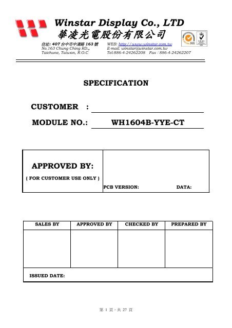
SPECIFICATION<br />
CUSTOMER :<br />
MODULE NO.:<br />
WH1604B-YYE-CT<br />
APPROVED BY:<br />
( FOR CUSTOMER USE ONLY )<br />
PCB VERSION:<br />
DATA:<br />
SALES BY APPROVED BY CHECKED BY PREPARED BY<br />
ISSUED DATE:<br />
第 1 頁 , 共 27 頁
Winstar Display Co., LTD<br />
華 凌 光 電 股 份 有 限 公 司<br />
RECORDS OF REVISION<br />
MODLE NO:<br />
DOC. FIRST ISSUE<br />
VERSION<br />
DATE<br />
REVISED<br />
PAGE NO. SUMMARY<br />
0 2006.06.06 First issue<br />
第 2 頁 , 共 27 頁
Contents<br />
1.Module Classification Information<br />
2.Precautions in use of LCD Modules<br />
3.General Specification<br />
4.Absolute Maximum Ratings<br />
5.Electrical Characteristics<br />
6.Optical Characteristics<br />
7.Interface Pin Function<br />
8.Contour Drawing & Block Diagram<br />
9.Function Description<br />
10.Character Generator ROM Pattern<br />
11.Instruction Table<br />
12.Timing Characteristics<br />
13.Initializing of LCM<br />
14.Reliability<br />
15.Backlight Information<br />
16. Inspection specification<br />
第 3 頁 , 共 27 頁
1.Module Classification Information<br />
W H 1 6 0 4 B-Y Y E- CT<br />
<br />
Brand:WINSTAR DISPLAY CORPORATION<br />
Display Type:H→Character Type, G→Graphic Type<br />
Display Font:Character 16 words, 4Lines.<br />
Model serials no.<br />
Backlight Type:<br />
N→Without backlight<br />
B→EL, Blue green<br />
D→EL, Green<br />
W→EL, White<br />
F→CCFL, White<br />
Y→LED, Yellow Green<br />
T→LED, White<br />
A→LED, Amber<br />
R→LED, Red<br />
O→LED, Orange<br />
G→LED, Green<br />
LCD Mode: B→TN Positive, Gray T→FSTN Negative<br />
N→TN Negative,<br />
G→STN Positive, Gray<br />
Y→STN Positive, Yellow Green<br />
M→STN Negative, Blue<br />
F→FSTN Positive<br />
LCD Polarizer<br />
Type/ Temperature<br />
range/ View<br />
direction<br />
Special Code<br />
A→Reflective, N.T, 6:00<br />
D→Reflective, N.T, 12:00<br />
G→Reflective, W. T, 6:00<br />
J→Reflective, W. T, 12:00<br />
B→Transflective, N.T,6:00<br />
E→Transflective, N.T.12:00<br />
CT : English and Cyrillic standard font<br />
H→Transflective, W.T,6:00<br />
K→Transflective, W.T,12:00<br />
C→Transmissive, N.T,6:00<br />
F→Transmissive, N.T,12:00<br />
I→Transmissive, W. T, 6:00<br />
L→Transmissive, W.T,12:00<br />
第 4 頁 , 共 27 頁
2.Precautions in use of LCD Modules<br />
(1)Avoid applying excessive shocks to the module or making any alterations or modifications to it.<br />
(2)Don’t make extra holes on the printed circuit board, modify its shape or change the components of<br />
LCD module.<br />
(3)Don’t disassemble the LCM.<br />
(4)Don’t operate it above the absolute maximum rating.<br />
(5)Don’t drop, bend or twist LCM.<br />
(6)Soldering: only to the I/O terminals.<br />
(7)Storage: please storage in anti-static electricity container and clean environment.<br />
3.General Specification<br />
Item Dimension Unit<br />
Number of Characters 16 characters x 4 Lines -<br />
Module dimension 70.6 x 60.0 x 13.5(MAX) mm<br />
View area 60.0 x 32.6 mm<br />
Active area 56.2 x 20.8 mm<br />
Dot size 0.55 x 0.55 mm<br />
Dot pitch 0.60 x 0.60 mm<br />
Character size 2.95 x 4.75 mm<br />
Character pitch 3.55 x 5.35 mm<br />
LCD type<br />
STN Positive, Transflective,Yellow Green<br />
Duty 1/16<br />
View direction<br />
Backlight Type<br />
12 o’clock<br />
LED, Yellow Green<br />
第 5 頁 , 共 27 頁
4.Absolute Maximum Ratings<br />
Item Symbol Min Typ Max Unit<br />
Operating Temperature T OP 0 - +50 ℃<br />
Storage Temperature T ST -10 - +60 ℃<br />
Input Voltage V I V SS - V DD V<br />
Supply Voltage For Logic VDD-V SS -0.3 - 7 V<br />
Supply Voltage For LCD V DD -V 0 -0.3 - 13 V<br />
5.Electrical Characteristics<br />
Item Symbol Condition Min Typ Max Unit<br />
Supply Voltage For Logic V DD -V SS - 4.5 5.0 5.5 V<br />
Supply Voltage For LCD V DD -V 0<br />
Ta=0℃<br />
Ta=25℃<br />
-<br />
-<br />
-<br />
4.5<br />
5.2<br />
-<br />
V<br />
V<br />
Ta=50℃<br />
3.9<br />
-<br />
-<br />
V<br />
Input High Volt. V IH - 0.7 V DD - V DD V<br />
Input Low Volt. V IL - V SS - 0.6 V<br />
Output High Volt. V OH - 3.9 - - V<br />
Output Low Volt. V OL - - - 0.4 V<br />
Supply Current I DD V DD =5V - 1.2 - mA<br />
第 6 頁 , 共 27 頁
6.Optical Characteristics<br />
Item Symbol Condition Min Typ Max Unit<br />
View Angle<br />
(V)θ CR≧2 20 - 40 deg<br />
(H)φ CR≧2 -30 - 30 deg<br />
Contrast Ratio CR - - 3 - -<br />
Response Time<br />
T rise - - 200 300 ms<br />
T fall - - 200 300 ms<br />
Definition of Operation Voltage (Vop) Definition of Response Time ( Tr , Tf )<br />
Intensity<br />
Selected Wave<br />
Non-selected<br />
Conition<br />
Selected Conition<br />
Non-selected<br />
Conition<br />
100%<br />
Non-selected Wave<br />
Intensity<br />
10%<br />
Cr Max<br />
Cr = Lon / Loff<br />
100%<br />
90%<br />
Vop<br />
Driving Voltage(V)<br />
Tr<br />
Tf<br />
[positive type]<br />
[positive type]<br />
Conditions :<br />
Operating Voltage : Vop<br />
Frame Frequency : 64 HZ<br />
Viewing Angle(θ,φ) : 0˚, 0˚<br />
Driving Waveform : 1/N duty , 1/a bias<br />
Definition of viewing angle(CR≧2)<br />
θf<br />
θl<br />
θb<br />
θr<br />
φ= 180˚<br />
φ= 270˚<br />
φ= 90˚<br />
φ= 0˚<br />
第 7 頁 , 共 27 頁
7.Interface Pin Function<br />
Pin No. Symbol Level Description<br />
1 V SS 0V Ground<br />
2 V DD 5.0V Supply Voltage for logic<br />
3 VO (Variable) Operating voltage for LCD<br />
4 RS H/L H: DATA, L: Instruction code<br />
5 R/W H/L H: Read(MPU→Module) L: Write(MPU→Module)<br />
6 E H,H→L Chip enable signal<br />
7 DB0 H/L Data bus line<br />
8 DB1 H/L Data bus line<br />
9 DB2 H/L Data bus line<br />
10 DB3 H/L Data bus line<br />
11 DB4 H/L Data bus line<br />
12 DB5 H/L Data bus line<br />
13 DB6 H/L Data bus line<br />
14 DB7 H/L Data bus line<br />
15 A/VEE LED+<br />
16 K LED-<br />
第 8 頁 , 共 27 頁
8.Contour Drawing &Block Diagram<br />
16.2<br />
22.1<br />
10.2<br />
60.0 0.3<br />
11.2 32.60(VA)<br />
7.5<br />
17.1 5.2<br />
2.5 20.80(AA)<br />
44.6<br />
50.0<br />
2.5<br />
P2.54*15=38.1 16.3<br />
20- 1.0<br />
1.0<br />
2.0<br />
16<br />
1<br />
56.20(AA)<br />
60.00(VA)<br />
65.6<br />
70.6 0.3<br />
2.5<br />
4- 3.0PTH<br />
4- 4.0PAD<br />
1.0<br />
7.2<br />
5.3<br />
2.5<br />
13.5<br />
9.0<br />
15.0<br />
8.5<br />
LED B/L<br />
1<br />
2<br />
3<br />
4<br />
5<br />
6<br />
7<br />
8<br />
9<br />
10<br />
11<br />
12<br />
13<br />
14<br />
15<br />
16<br />
Vss<br />
Vdd<br />
Vo<br />
RS<br />
R/W<br />
E<br />
DB0<br />
DB1<br />
DB2<br />
DB3<br />
DB4<br />
DB5<br />
DB6<br />
DB7<br />
A/Vee<br />
K<br />
0.6<br />
0.55<br />
2.95 0.6<br />
The non-specified tolerance of dimension is 0.3mm.<br />
4.75<br />
0.6<br />
0.55<br />
0.6<br />
DOT SIZE<br />
LED B/L Drive Method<br />
1.Drive from A,K<br />
MPU<br />
80 series<br />
or<br />
68 series<br />
RS<br />
R/W<br />
E<br />
DB0~DB7<br />
Controller/Com Driver<br />
HD44780<br />
or<br />
Equivalent<br />
Com1~16<br />
Com17~32<br />
16X4 LCD<br />
R<br />
A<br />
K<br />
B/L<br />
2.Drive from pin15, pin16<br />
VR<br />
10K~20K<br />
Vdd<br />
Vo<br />
Vss<br />
Vee<br />
External contrast adjustment.<br />
Bias and<br />
Power Circuit<br />
N.V.<br />
Generator<br />
Optional<br />
Seg1~40<br />
D<br />
M<br />
CL1<br />
CL2<br />
Vdd,Vss,V1~V5<br />
Seg41~80<br />
Seg Driver<br />
Seg80~160<br />
Seg Driver<br />
R R A<br />
B/L<br />
K<br />
LCM<br />
(Will never get Vee output from pin15)<br />
3.Drive from Vdd,Vss<br />
R<br />
A<br />
K B/L<br />
LCM<br />
(Contrast performance may go down.)<br />
Recommanded Value<br />
VLED= 4.5V, ILED= 220mA<br />
R= 3.6Ω(1/2 Watt)<br />
Character located<br />
DDRAM address<br />
DDRAM address<br />
DDRAM address<br />
DDRAM address<br />
1 2 3 4 5 6 7 8 9 1011 12 13 1415<br />
16<br />
00 01 02 03 04 05 06 07 08 09 0A0B0C0D0E<br />
0F<br />
40 41 42 43 44 45 46 47 48 49 4A4B4C4D4E<br />
4F<br />
10 11 12 13 14 15 16 17 18 19 1A1B1C1D1E 1F<br />
50 51 52 53 54 55 56 57 58 59 5A5B5C5D5E<br />
5F<br />
第 9 頁 , 共 27 頁
9.Function Description<br />
The LCD display Module is built in a LSI controller, the controller has two 8-bit registers, an<br />
instruction register (IR) and a data register (DR).<br />
The IR stores instruction codes, such as display clear and cursor shift, and address information for<br />
display data RAM (DDRAM) and character generator (CGRAM). The IR can only be written from the<br />
MPU. The DR temporarily stores data to be written or read from DDRAM or CGRAM. When<br />
address information is written into the IR, then data is stored into the DR from DDRAM or CGRAM.<br />
By the register selector (RS) signal, these two registers can be selected.<br />
RS R/W Operation<br />
0 0 IR write as an internal operation (display clear, etc.)<br />
0 1 Read busy flag (DB7) and address counter (DB0 to DB7)<br />
1 0 Write data to DDRAM or CGRAM (DR to DDRAM or CGRAM)<br />
1 1 Read data from DDRAM or CGRAM (DDRAM or CGRAM to DR)<br />
Busy Flag (BF)<br />
When the busy flag is 1, the controller LSI is in the internal operation mode, and the next instruction<br />
will not be accepted. When RS=0 and R/W=1, the busy flag is output to DB7. The next instruction<br />
must be written after ensuring that the busy flag is 0.<br />
Address Counter (AC)<br />
The address counter (AC) assigns addresses to both DDRAM and CGRAM<br />
Display Data RAM (DDRAM)<br />
This DDRAM is used to store the display data represented in 8-bit character codes. Its extended<br />
capacity is 80×8 bits or 80 characters. Below figure is the relationships between DDRAM addresses<br />
and positions on the liquid crystal display.<br />
High bits<br />
Low bits<br />
Example: DDRAM addresses 4E<br />
AC<br />
(hexadecimal)<br />
AC6 AC5 AC4 AC3 AC2 AC1 AC0 1 0 0 1 1 1 0<br />
第 10 頁 , 共 27 頁
Display position DDRAM address<br />
1 2 3 4 5 6 7 8 9 10 11 12 13 14 15 16<br />
00 01 02 03 04 05 06 07 08 09 0A 0B 0C 0D 0E 0F<br />
40 41 42 43 44 45 46 47 48 49 4A 4B 4C 4D 4E 4F<br />
10 11 12 13 14 15 16 17 18 19 1A 1B 1C 1D 1E 1F<br />
50 51 52 53 54 55 56 57 58 59 5A 5B 5C 5D 5E 5F<br />
4-Line by 16-Character Display<br />
Character Generator ROM (CGROM)<br />
The CGROM generate 5×8 dot or 5×10 dot character patterns from 8-bit character codes. See Table 2.<br />
Character Generator RAM (CGRAM)<br />
In CGRAM, the user can rewrite character by program. For 5×8 dots, eight character patterns can be<br />
written, and for 5×10 dots, four character patterns can be written.<br />
Write into DDRAM the character code at the addresses shown as the left column of table 1. To show<br />
the character patterns stored in CGRAM.<br />
第 11 頁 , 共 27 頁
Relationship between CGRAM Addresses, Character Codes (DDRAM) and Character patterns<br />
Table 1.<br />
For 5 * 8 dot character patterns<br />
Character Codes<br />
( DDRAM data )<br />
CGRAM Address<br />
Character Patterns<br />
( CGRAM data )<br />
7 6 5 4 3 2 1 0<br />
5 4 3 2 1 0 7 6 5 4 3 2 1 0<br />
H igh L ow H igh L ow H igh L ow<br />
0 0 0 * * *<br />
0<br />
0 0 1 * * * 0 0 0<br />
0 1 0 * * * 0 0 0<br />
0 1 1 * * *<br />
0<br />
0 0 0 0 * 0 0 0<br />
0 0 0 1 0 0 * * * 0 0 0<br />
1 0 1 * * * 0 0 0<br />
1 1 0 * * * 0 0 0<br />
1 1 1 * * * 0 0 0 0 0<br />
0 0 0 * * * 0 0 0<br />
0 0 1 * * * 0 0 0<br />
0 1 0 * * *<br />
0 1 1 * * * 0 0 0 0<br />
0 0 0 0 * 0 0 1<br />
0 0 1 1 0 0 * * *<br />
1 0 1 * * * 0 0 0 0<br />
1 1 0 * * * 0 0 0 0<br />
1 1 1 * * * 0 0 0 0 0<br />
0 0 0 * * *<br />
0 0 1<br />
Character<br />
pattern( 1 )<br />
Cursor pattern<br />
Character<br />
pattern( 2 )<br />
Cursor pattern<br />
0 0 0 0 * 1 1 1<br />
For 5 * 10 dot character patterns<br />
Character Codes<br />
( DDRAM data )<br />
1 1 1 1 0 0<br />
1 0 1<br />
1 1 0<br />
1 1 1<br />
CGRAM Address<br />
* * *<br />
Character Patterns<br />
( CGRAM data )<br />
7<br />
6 5 4 3 2 1 0<br />
H igh<br />
L ow<br />
H igh<br />
0 0 0 0 * 0 0 0 0 0<br />
5 4 3 2 1 0<br />
L ow<br />
0 0 0 0<br />
0 0 0 1<br />
0 0 1 0<br />
0 0 1 1<br />
0 1 0 0<br />
0 1 0 1<br />
0 1 1 0<br />
0 1 1 1<br />
1 0 0 0<br />
1 0 0 1<br />
1 0 1 0<br />
7 6 5 4 3 2 1 0<br />
H igh<br />
L ow<br />
* * * 0 0 0 0 0<br />
* * * 0 0 0 0 0<br />
* * * 0 0<br />
* * * 0 0<br />
* * * 0 0 0<br />
* * * 0 0 0<br />
* * *<br />
0<br />
* * * 0 0 0 0<br />
* * * 0 0 0 0<br />
* * * 0 0 0 0<br />
* * * 0 0 0 0 0<br />
Character<br />
pattern<br />
Cursor pattern<br />
: " H igh "<br />
1 1 1 1<br />
* * * * * * * *<br />
第 12 頁 , 共 27 頁
10.Character Generator ROM Pattern<br />
Table.2<br />
Upper<br />
4 bit<br />
Lower<br />
4 bit<br />
LLLL<br />
LLLH<br />
LLHL<br />
LLHH<br />
LHLL<br />
LHLH<br />
LHHL<br />
LHHH<br />
HLLL<br />
HLLH<br />
HLHL<br />
HLHH<br />
HHLL<br />
HHLH<br />
HHHL<br />
HHHH<br />
LLLL LLLH LLHL LLHH LHLL LHLH LHHL LHHH HLLL HLLH HLHL HLHH HHLL HHLH HHHL HHHH<br />
CG<br />
RAM<br />
(1)<br />
CG<br />
RAM<br />
(2)<br />
CG<br />
RAM<br />
(3)<br />
CG<br />
RAM<br />
(4)<br />
CG<br />
RAM<br />
(5)<br />
CG<br />
RAM<br />
(6)<br />
CG<br />
RAM<br />
(7)<br />
CG<br />
RAM<br />
(8)<br />
CG<br />
RAM<br />
(1)<br />
CG<br />
RAM<br />
(2)<br />
CG<br />
RAM<br />
(3)<br />
CG<br />
RAM<br />
(4)<br />
CG<br />
RAM<br />
(5)<br />
CG<br />
RAM<br />
(6)<br />
CG<br />
RAM<br />
(7)<br />
CG<br />
RAM<br />
(8)<br />
第 13 頁 , 共 27 頁
11.Instruction Table<br />
Instruction<br />
Instruction Code<br />
RS R/W DB7 DB6 DB5 DB4 DB3 DB2 DB1 DB0<br />
Description<br />
Execution time<br />
(fosc=270Khz)<br />
Clear Display 0 0 0 0 0 0 0 0 0 1<br />
Write “00H” to DDRAM and set<br />
DDRAM address to “00H” from AC<br />
1.53ms<br />
Return Home 0 0 0 0 0 0 0 0 1 -<br />
Entry Mode<br />
Set<br />
Display<br />
ON/OFF<br />
Control<br />
0 0 0 0 0 0 0 1 I/D SH<br />
0 0 0 0 0 0 1 D C B<br />
Set DDRAM address to “00H” from AC<br />
and return cursor to its original position<br />
if shifted. The contents of DDRAM are<br />
not changed.<br />
Assign cursor moving direction and<br />
enable the shift of entire display.<br />
Set display (D), cursor (C), and blinking<br />
of cursor (B) on/off control bit.<br />
1.53ms<br />
Set cursor moving and display shift<br />
Cursor or<br />
0 0 0 0 0 1 S/C R/L - - control bit, and the direction, without<br />
Display Shift<br />
changing of DDRAM data.<br />
39μs<br />
Set interface data length<br />
(DL:8-bit/4-bit), numbers of display line<br />
Function Set 0 0 0 0 1 DL N F - -<br />
(N:2-line/1-line)and, display font type<br />
39μs<br />
(F:5×11 dots/5×8 dots)<br />
Set CGRAM<br />
Address<br />
0 0 0 1 AC5 AC4 AC3 AC2 AC1 AC0 Set CGRAM address in address counter. 39μs<br />
Set DDRAM<br />
Address<br />
0 0 1 AC6 AC5 AC4 AC3 AC2 AC1 AC0 Set DDRAM address in address counter. 39μs<br />
Whether during internal operation or not<br />
Read Busy<br />
can be known by reading BF. The<br />
Flag and 0 1 BF AC6 AC5 AC4 AC3 AC2 AC1 AC0<br />
contents of address counter can also be<br />
Address<br />
read.<br />
0μs<br />
Write Data to<br />
Write data into internal RAM<br />
1 0 D7 D6 D5 D4 D3 D2 D1 D0<br />
RAM<br />
(DDRAM/CGRAM).<br />
43μs<br />
39μs<br />
39μs<br />
Read Data<br />
from RAM<br />
1 1 D7 D6 D5 D4 D3 D2 D1 D0<br />
Read data from internal RAM<br />
(DDRAM/CGRAM).<br />
43μs<br />
* ”-”:don’t care<br />
第 14 頁 , 共 27 頁
12.Timing Characteristics<br />
12.1 Write Operation<br />
Ta=25℃, VDD=5.0V<br />
Item Symbol Min Typ Max Unit<br />
Enable cycle time T C 1200 - - ns<br />
Enable pulse width T PW 140 - - ns<br />
Enable rise/fall time T R ,T F - - 25 ns<br />
Address set-up time (RS, R/W to E) t AS 0 - - ns<br />
Address hold time t AH 10 - - ns<br />
Data set-up time t DSW 40 - - ns<br />
Data hold time t H 10 - - ns<br />
第 15 頁 , 共 27 頁
12.2 Read Operation<br />
Ta=25℃, VDD=5V<br />
Item Symbol Min Typ Max Unit<br />
Enable cycle time T C 1200 - - ns<br />
Enable pulse width (high level)<br />
T PW 140 - - ns<br />
Enable rise/fall time T R ,T F - - 25 ns<br />
Address set-up time (RS, R/W to E) t AS 0 - - ns<br />
Address hold time t AH 10 - - ns<br />
Data delay time t DDR - - 100 ns<br />
Data hold time t H 10 - - ns<br />
第 16 頁 , 共 27 頁
13.Initializing of LCM<br />
Power on<br />
Wait for more than 40 ms after VDD rises to 4.5 V<br />
RS<br />
0<br />
R/W<br />
0<br />
DB7 DB6<br />
0 0<br />
DB5 DB4 DB3<br />
1 1 *<br />
DB2<br />
*<br />
DB1<br />
*<br />
DB0<br />
*<br />
BF can not be checked before this instruction.<br />
Function set<br />
RS<br />
0<br />
0<br />
R/W<br />
0<br />
0<br />
Wait for more than 39us<br />
DB7 DB6<br />
0 0<br />
N F<br />
DB5 DB4 DB3 DB2 DB1 DB0<br />
1 0 * * * *<br />
* * * * * *<br />
BF can not be checked before this instruction.<br />
Function set<br />
Wait for more than 39 s<br />
RS<br />
0<br />
0<br />
R/W DB7 DB6 DB5 DB4 DB3 DB2 DB1 DB0<br />
BF can not be checked before this instruction.<br />
0 0 0 1 0 * * * *<br />
0 N F * * * * * *<br />
Function set<br />
Wait for more than 37us<br />
RS<br />
0<br />
0<br />
R/W<br />
0<br />
0<br />
DB7<br />
0<br />
1<br />
DB6<br />
0<br />
D<br />
DB5<br />
0<br />
C<br />
DB4<br />
0<br />
B<br />
DB3<br />
*<br />
*<br />
DB2<br />
*<br />
*<br />
DB1<br />
*<br />
*<br />
DB0<br />
*<br />
*<br />
Display ON/OFF control<br />
Wait for more than 37 s<br />
RS<br />
0<br />
0<br />
R/W<br />
0<br />
0<br />
DB7 DB6 DB5 DB4 DB3 DB2 DB1 DB0<br />
0 0 0 0 * * * *<br />
0 0 0 1 * * * *<br />
Display Clear<br />
Wait for more than 1ms<br />
RS<br />
0<br />
0<br />
R/W<br />
0<br />
0<br />
DB7 DB6 DB5 DB4 DB3 DB2 DB1 DB0<br />
0 0 0 0 * * * *<br />
0 1 I/D SH * * * *<br />
Entry Mode Set<br />
Initialization ends<br />
4-Bit Ineterface<br />
第 17 頁 , 共 27 頁
Power on<br />
Wait for more than 40 ms after VDD rises to 4.5 V<br />
RS R/WDB7 DB6 DB5 DB4 DB3 DB2 DB1 DB0<br />
0 0 0 0 1 1 N F * *<br />
BF can not be checked before this instruction.<br />
Function set<br />
Wait for more than 39us<br />
RS R/WDB7<br />
0 0 0<br />
DB6<br />
0<br />
DB5<br />
1<br />
DB4 DB3 DB2 DB1 DB0<br />
1 N F * *<br />
BF can not be checked before this instruction.<br />
Function set<br />
Wait for more than 37us<br />
RS R/W DB7 DB6 DB5 DB4 DB3 DB2 DB1 DB0<br />
0 0 0 0 0 0 1 B C D<br />
Display ON/OFF control<br />
Wait for more than 37 s<br />
RS<br />
0<br />
R/W<br />
0<br />
DB7<br />
0 0<br />
DB6 DB5 DB4 DB3 DB2 DB1<br />
0 0 0 0 0<br />
DB0<br />
1<br />
Display Clear<br />
Wait for more than 1ms<br />
RS<br />
0<br />
R/W<br />
0<br />
DB7 DB6 DB5 DB4 DB3 DB2 DB1 DB0<br />
0 0 0 0 0 1 I/D S<br />
Entry Mode Set<br />
Initialization ends<br />
8-Bit Ineterface<br />
第 18 頁 , 共 27 頁
14.Reliability<br />
Content of Reliability Test ( Normal temperature, 0℃~50℃)<br />
Environmental Test<br />
Test Item Content of Test Test Condition Note<br />
High Temperature Endurance test applying the high storage<br />
60℃<br />
storage<br />
temperature for a long time.<br />
200hrs<br />
2<br />
Low Temperature Endurance test applying the high storage -10℃<br />
storage<br />
temperature for a long time.<br />
200hrs<br />
1,2<br />
Endurance test applying the electric stress<br />
High Temperature<br />
50℃<br />
(Voltage & Current) and the thermal stress to the<br />
Operation<br />
200hrs<br />
element for a long time.<br />
——<br />
Low Temperature<br />
Operation<br />
High Temperature/<br />
Humidity Operation<br />
Thermal shock<br />
resistance<br />
Vibration test<br />
Static electricity test<br />
Endurance test applying the electric stress under<br />
low temperature for a long time.<br />
The module should be allowed to stand at 40<br />
℃,90%RH max<br />
For 96hrs under no-load condition excluding the<br />
polarizer,<br />
Then taking it out and drying it at normal<br />
temperature.<br />
The sample should be allowed stand the<br />
following 10 cycles of<br />
operation<br />
0℃ 25℃ 50℃<br />
30min 5min 30min<br />
1 cycle<br />
Endurance test applying the vibration during<br />
transportation and using.<br />
Endurance test applying the electric stress to the<br />
terminal.<br />
0℃<br />
200hrs<br />
40℃,90%RH<br />
96hrs<br />
0℃/ 50℃<br />
10 cycles<br />
Total fixed<br />
amplitude : 1.5mm<br />
Vibration<br />
Frequency :<br />
10~55Hz<br />
One cycle 60<br />
seconds to 3<br />
directions of X,Y,Z<br />
for Each<br />
15 minutes<br />
VS=800V,RS=1.5k<br />
Ω<br />
CS=100pF<br />
1 time<br />
Note1: No dew condensation to be observed.<br />
Note2: The function test shall be conducted after 4 hours storage at the normal<br />
Temperature and humidity after remove from the test chamber.<br />
Note3: Vibration test will be conducted to the product itself without putting it in a container.<br />
1<br />
1,2<br />
——<br />
3<br />
——<br />
第 19 頁 , 共 27 頁
15.Backlight Information<br />
Specification<br />
PARAMETER SYMBOL MIN TYP MAX UNIT TEST CONDITION<br />
Supply Current ILED 176 220 330 mA V=4.2V<br />
Supply Voltage V 4.0 4.2 4.4 V -<br />
Reverse Voltage VR - - 8 V -<br />
Luminous<br />
Intensity<br />
IV 60 - - CD/M 2 ILED=220mA<br />
Wave Length λp ─ 573 - nm ILED=220mA<br />
Life Time - - 100000 - Hr. ILED=220mA<br />
Color<br />
Yellow Green<br />
Note: The LED of B/L is drive by current only, drive voltage is for reference only.<br />
drive voltage can make driving current under safety area (current between<br />
minimum and maximum).<br />
第 20 頁 , 共 27 頁
16. Inspection specification<br />
NO Item Criterion AQL<br />
01<br />
Electrical<br />
Testing<br />
1.1 Missing vertical, horizontal segment, segment contrast defect.<br />
1.2 Missing character , dot or icon.<br />
1.3 Display malfunction.<br />
1.4 No function or no display.<br />
1.5 Current consumption exceeds product specifications.<br />
1.6 LCD viewing angle defect.<br />
1.7 Mixed product types.<br />
1.8 Contrast defect.<br />
0.65<br />
02<br />
Black or white<br />
spots on LCD<br />
(display only)<br />
2.1 White and black spots on display ≦0.25mm, no more than<br />
three white or black spots present.<br />
2.2 Densely spaced: No more than two spots or lines within 3mm<br />
2.5<br />
3.1 Round type : As following drawing<br />
Φ=( x + y ) / 2 SIZE Acceptable Q TY<br />
Φ≦0.10 Accept no dense<br />
0.10
NO Item Criterion AQL<br />
05 Scratches Follow NO.3 LCD black spots, white spots, contamination<br />
Symbols Define:<br />
x: Chip length y: Chip width z: Chip thickness<br />
k: Seal width t: Glass thickness a: LCD side length<br />
L: Electrode pad length:<br />
6.1 General glass chip :<br />
6.1.1 Chip on panel surface and crack between panels:<br />
z: Chip thickness y: Chip width x: Chip length<br />
06<br />
Chipped<br />
glass<br />
Z≦1/2t Not over viewing x≦1/8a<br />
area<br />
1/2t
NO Item Criterion<br />
Symbols :<br />
x: Chip length y: Chip width z: Chip thickness<br />
k: Seal width t: Glass thickness a: LCD side length<br />
L: Electrode pad length<br />
6.2 Protrusion over terminal :<br />
6.2.1 Chip on electrode pad :<br />
AQL<br />
y: Chip width x: Chip length z: Chip thickness<br />
y≦0.5mm x≦1/8a 0 < z ≦ t<br />
6.2.2 Non-conductive portion:<br />
06<br />
Glass<br />
crack<br />
2.5<br />
y: Chip width x: Chip length z: Chip thickness<br />
y≦ L x≦1/8a 0 < z ≦ t<br />
☉If the chipped area touches the ITO terminal, over 2/3 of the ITO must<br />
remain and be inspected according to electrode terminal specifications.<br />
☉If the product will be heat sealed by the customer, the alignment mark<br />
not be damaged.<br />
6.2.3 Substrate protuberance and internal crack.<br />
y: width x: length<br />
y≦1/3L<br />
x ≦ a<br />
第 23 頁 , 共 27 頁
NO Item Criterion AQL<br />
07 Cracked glass The LCD with extensive crack is not acceptable. 2.5<br />
08<br />
Backlight<br />
elements<br />
8.1 Illumination source flickers when lit.<br />
8.2 Spots or scratched that appear when lit must be judged. Using<br />
LCD spot, lines and contamination standards.<br />
8.3 Backlight doesn’t light or color wrong.<br />
0.65<br />
2.5<br />
0.65<br />
09 Bezel<br />
9.1 Bezel may not have rust, be deformed or have fingerprints,<br />
stains or other contamination.<br />
9.2 Bezel must comply with job specifications.<br />
2.5<br />
0.65<br />
10 PCB、COB<br />
10.1 COB seal may not have pinholes larger than 0.2mm or 2.5<br />
contamination.<br />
10.2 COB seal surface may not have pinholes through to the IC.<br />
2.5<br />
0.65<br />
10.3 The height of the COB should not exceed the height<br />
indicated in the assembly diagram.<br />
2.5<br />
10.4 There may not be more than 2mm of sealant outside the<br />
seal area on the PCB. And there should be no more than<br />
three places.<br />
2.5<br />
10.5 No oxidation or contamination PCB terminals.<br />
0.65<br />
10.6 Parts on PCB must be the same as on the production<br />
characteristic chart. There should be no wrong parts,<br />
missing parts or excess parts.<br />
0.65<br />
10.7 The jumper on the PCB should conform to the product<br />
characteristic chart.<br />
2.5<br />
10.8 If solder gets on bezel tab pads, LED pad, zebra pad or<br />
screw hold pad, make sure it is smoothed down.<br />
2.5<br />
10.9 The Scraping testing standard for Copper Coating of PCB<br />
X<br />
Y<br />
X * Y
NO Item Criterion AQL<br />
12<br />
General<br />
appearance<br />
12.1 No oxidation, contamination, curves or, bends on interface Pin<br />
(OLB) of TCP.<br />
12.2 No cracks on interface pin (OLB) of TCP.<br />
12.3 No contamination, solder residue or solder balls on product.<br />
12.4 The IC on the TCP may not be damaged, circuits.<br />
12.5 The uppermost edge of the protective strip on the interface pin<br />
must be present or look as if it cause the interface pin to sever.<br />
12.6 The residual rosin or tin oil of soldering (component or chip<br />
component) is not burned into brown or black color.<br />
12.7 Sealant on top of the ITO circuit has not hardened.<br />
12.8 Pin type must match type in specification sheet.<br />
12.9 LCD pin loose or missing pins.<br />
12.10 Product packaging must the same as specified on packaging<br />
specification sheet.<br />
12.11 Product dimension and structure must conform to product<br />
specification sheet.<br />
2.5<br />
0.65<br />
2.5<br />
2.5<br />
2.5<br />
2.5<br />
2.5<br />
0.65<br />
0.65<br />
0.65<br />
0.65<br />
第 25 頁 , 共 27 頁
winstar LCM Sample Estimate Feedback Sheet<br />
Module Number: Page: 1<br />
1、Panel Specification:<br />
1. Panel Type: □ Pass □ NG ,<br />
2. View Direction: □ Pass □ NG ,<br />
3. Numbers of Dots: □ Pass □ NG ,<br />
4. View Area: □ Pass □ NG ,<br />
5. Active Area: □ Pass □ NG ,<br />
6. Operating Temperature: □ Pass □ NG ,<br />
7. Storage Temperature: □ Pass □ NG ,<br />
8. Others:<br />
2、Mechanical Specification:<br />
1. PCB Size: □ Pass □ NG ,<br />
2. Frame Size: □ Pass □ NG ,<br />
3. Materal of Frame: □ Pass □ NG ,<br />
4. Connector Position: □ Pass □ NG ,<br />
5. Fix Hole Position: □ Pass □ NG ,<br />
6. Backlight Position: □ Pass □ NG ,<br />
7. Thickness of PCB: □ Pass □ NG ,<br />
8. Height of Frame to PCB: □ Pass □ NG ,<br />
9. Height of Module: □ Pass □ NG ,<br />
10. Others: □ Pass □ NG ,<br />
3、Relative Hole Size:<br />
1. Pitch of Connector: □ Pass □ NG ,<br />
2. Hole size of Connector: □ Pass □ NG ,<br />
3. Mounting Hole size: □ Pass □ NG ,<br />
4. Mounting Hole Type: □ Pass □ NG ,<br />
5. Others: □ Pass □ NG ,<br />
4、Backlight Specification:<br />
1. B/L Type: □ Pass □ NG ,<br />
2. B/L Color: □ Pass □ NG ,<br />
3. B/L Driving Voltage (Reference for LED Type): □ Pass □ NG ,<br />
4. B/L Driving Current: □ Pass □ NG ,<br />
5. Brightness of B/L: □ Pass □ NG ,<br />
6. B/L Solder Method: □ Pass □ NG ,<br />
7. Others: □ Pass □ NG ,<br />
>> Go to page 2
winstar<br />
Module Number: Page: 2<br />
5、Electronic Characteristics of Module:<br />
1. Input Voltage: □ Pass □ NG ,<br />
2. Supply Current: □ Pass □ NG ,<br />
3. Driving Voltage for LCD: □ Pass □ NG ,<br />
4. Contrast for LCD: □ Pass □ NG ,<br />
5. B/L Driving Method: □ Pass □ NG ,<br />
6. Negative Voltage Output: □ Pass □ NG ,<br />
7. Interface Function: □ Pass □ NG ,<br />
8. LCD Uniformity: □ Pass □ NG ,<br />
9. ESD test: □ Pass □ NG ,<br />
10. Others: □ Pass □ NG ,<br />
6、Summary:<br />
Sales signature:<br />
Customer Signature: Date: / /<br />
第 27 頁 , 共 27 頁


