Tunnel Diode - Quantum Device Lab
Tunnel Diode - Quantum Device Lab
Tunnel Diode - Quantum Device Lab

You also want an ePaper? Increase the reach of your titles
YUMPU automatically turns print PDFs into web optimized ePapers that Google loves.
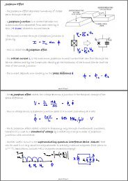
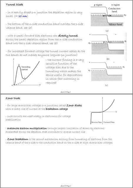
<strong>Tunnel</strong> <strong>Diode</strong><br />
- in a heavily doped p-n junction the depletion region is very<br />
small (~ 10 nm)<br />
- the bottom of the n-side conduction band overlaps the p-side<br />
valence band, see (a)<br />
- with a small forward bias electrons can directly tunnel<br />
across the small depletion region from the n-side conduction<br />
band into the p side valence band, see (b)<br />
- for increased forward voltage the tunnel current ceases as the<br />
two bands do not overlap anymore (regular pn junction)<br />
- the current flowing is a very<br />
sensitive function of the<br />
voltage bias due to the<br />
tunneling which makes the<br />
device useful for applications<br />
in which fast switching is<br />
required<br />
phys4.19 Page 1<br />
Zener <strong>Diode</strong><br />
- for large reverse bias voltages p-n junctions called Zener diodes<br />
show a sharp rise of current at the breakdown voltage<br />
- such circuits are used widely in electronics for voltage<br />
stabilization<br />
- avalanche electron multiplication through impact ionization of atoms by electrons<br />
accelerated across the depletion area contribute to reverse current rise<br />
- Zener breakdown is the second mechanism arising from tunneling of electrons from the<br />
valence band of the p-side to the conduction band on the n-side at high reverse bias voltages<br />
phys4.19 Page 2
npn-Junction Transistor<br />
- consists of a thin p-doped region called the<br />
base electrode connected to an n-doped<br />
emitter and collector electrode, see figure<br />
- an npn transistor acts as an amplifier for small signals applied between the emitter and<br />
base electrode that are amplified into a large base-collector signals<br />
- the energy band structure of the npn<br />
transistor at zero bias is shown<br />
- the current in an npn transistor is carried<br />
by electrons<br />
- a pnp transistor would work in an analog<br />
way for holes being the predominant charge<br />
carrier<br />
phys4.19 Page 3<br />
Transistor Bias<br />
- for transistor operation the emitter base<br />
junction is weakly forward biased and the<br />
base collector junction is strongly reverse<br />
biased<br />
- the current from the heavily doped emitter into<br />
the base is carried by electrons<br />
- electrons diffuse across the thin (~ 1 μm) weakly hole doped base electrode into the baseemitter<br />
junction and are accelerated by the large reverse bias into the collector<br />
- the input signal power is then amplified at constant current by the large base collector<br />
reverse bias voltage to a larger output power<br />
- a limitation of the npn transistor amplifier is its low input impedance (or low input<br />
resistance), also its power consumption and integration density are not the best<br />
- for some applications an amplifier with higher input impedance, such as a field effect<br />
transistor, is advantageous<br />
phys4.19 Page 4
Field Effect Transistor (FET)<br />
- an FET consists of a n-type channel<br />
connecting source and drain and contacted by<br />
a p-type gate; it is widely used as an<br />
alternative to npn junction transistors<br />
- electrons move from source to drain along an n-type channel<br />
- the pn junction is reverse biased to create a depletion region at the interface, the carrier<br />
density and the source-drain current depend sensitively on the magnitude of the reverse bias<br />
- in reverse bias little current flows into the pn junction giving it a high input impedance<br />
Metal Oxide Semiconductor Field Effect Transistor (MOSFET)<br />
- semiconductor gate replaced by a metal film separated from the channel by a thin oxide<br />
layer<br />
- MOSFETs have high input impedance (up to 10 15 Ω) due to capacitively coupled gate and<br />
are also compatible with high integration density<br />
phys4.19 Page 5<br />
Superconductivity<br />
- usual electrical conductors, even the very best ones, have finite resistance determined by<br />
temperature and impurities in the material<br />
- at very low temperatures some metals, alloys and some special chemical compounds can<br />
transport current without resistance, an effect called superconductivity<br />
- Kammerlingh Onnes discovered that resistance of<br />
mercury (Hg) decreased like that of other metals down<br />
to T c ~ 4.15 K but then lost all of its resistance to<br />
immeasurable levels below that critical temperature T c<br />
- the resistivity is actually zero as tested in persistent<br />
current measurements<br />
- usual critical temperatures for metallic<br />
superconductors are in the range 0.1 - 10 K<br />
- it is interesting to note that good usual conductors<br />
such as copper (Cu) and silver (Ag) do not become<br />
superconducting<br />
phys4.19 Page 6
The Nobel Prize in Physics 1913<br />
"for his investigations on the properties of matter at low<br />
temperatures which led, inter alia, to the production of liquid<br />
helium"<br />
Leiden University, Leiden, the Netherlands<br />
Heike Kamerlingh Onnes<br />
b. 1853, d. 1926<br />
The Nobel Prize in Physics 1987<br />
"for their important break-through in the<br />
discovery of superconductivity in ceramic<br />
materials"<br />
IBM Zurich Research <strong>Lab</strong>oratory<br />
Rüschlikon, Switzerland<br />
J. Georg Bednorz<br />
Germany<br />
b. 1950<br />
K. Alexander Müller<br />
Switzerland<br />
b. 1927<br />
phys4.19 Page 7<br />
Magnetic Effects<br />
- the critical temperature T c of a superconductor<br />
depends on the magnetic field (see figure)<br />
- in a type I superconductor the zero resistance<br />
state disappears altogether at a threshold critical<br />
field B c that depends on the material and the<br />
temperature<br />
- the maximum critical field occurs at zero<br />
temperature<br />
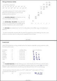
Superconductor T c and B c<br />
- because of the limited critical fields of type I<br />
superconductors they are of limited use in<br />
applications for field generation with coils<br />
material T c [K] B c [T]<br />
Al 1.18 0.015<br />
Hg 4.15 0.041<br />
In 3.41 0.028<br />
Pb 7.19 0.080<br />
Sn 3.72 0.031<br />
Zn 0.85 0.005<br />
phys4.19 Page 8
Meissner Effect<br />
- superconductors are perfectly diamagnetic<br />
- in a type I superconductor field below the<br />
critical field is expelled completely from the<br />
material when cooled through T c , see figure<br />
- in this Meissner effect screening currents<br />
are induced in the superconductor to cancel the<br />
externally applied field<br />
- this effect distinguishes a superconductor from an ideal conductor<br />
- type II superconductors below a first critical field Bc1 behave like type I superconductors,<br />
above B c1 and below a second critical field B c2 magnetic flux can penetrate into the material<br />
bringing it to a mixed superconducting/normal state<br />
- B c2 critical fields can be high so that these<br />
materials are interesting for generating<br />
magnetic fields<br />
material T c [K] B c2 [T]<br />
Nb 3 Sn 18.0 24.5<br />
phys4.19 Page 9<br />
Cooper Pairs and Bardeen-Cooper-Schrieffer (BCS) theory<br />
- in conventional superconductors electrons attract each other through deformations induced<br />
in the crystal lattice<br />
- materials with strong lattice vibrations are usually poor conductors at room temperature but<br />
maybe superconductors at low temperatures<br />
- a hint of this fact was first found when it was noted that the T c of different superconductors<br />
depends on the isotope used, e.g. T c ( 199 Hg) = 4.161 and T c ( 204 Hg) = 4.126<br />
- two electrons (Fermions) form a single Cooper pair (Boson) with the electrons being in a<br />
singlet state with zero angular momentum<br />
- the binding energy E g , also called the gap energy, is<br />
typically on the order of 1 meV and can be measured using<br />
microwave absorption<br />
- at temperatures above 0 K some Cooper pairs are broken up<br />
by thermal fluctuations, the remaining electrons interact<br />
with the Cooper pairs effectively reducing the gap energy<br />
(see figure)<br />
phys4.19 Page 10
- at the critical temperature T c the energy gap disappears, there are no more Cooper pairs and<br />
thus the material ceases to be superconducting<br />
- electrons (fermions) in a superconductor form Cooper pairs with<br />
total spin S = 0<br />
- the Cooper pair is a boson, any number of bosons can be in the same quantum state ψ<br />
- Cooper pairs in a super conductor form a Bose-Einstein condensate<br />
- all Cooper pairs in a superconductor are described by a single macroscopic wave function<br />
minimizing the system energy<br />
where ρ is the Cooper pair density and φ their phase<br />
- when a current flows in a superconductor, all Cooper pairs have the same non-zero linear<br />
momentum<br />
- no scattering of individual electrons that would lead to finite resistance can occur<br />
phys4.19 Page 11<br />
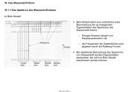
Flux Quantization<br />
- Faraday's law relates the current I flowing through a<br />
loop enclosing an area A and the magnetic flux Φ = A B<br />
in the loop<br />
- the flux Φ in the superconductor is quantized because<br />
the wave function describing the Cooper pairs in the ring<br />
must be a continuous periodic function around the loop<br />
(compare to Bohr model)<br />
- the flux quantization rule is<br />
- with the magnetic flux quantum<br />
phys4.19 Page 12