TM-271A Service manual - The Repeater Builder's Technical ...
TM-271A Service manual - The Repeater Builder's Technical ...
TM-271A Service manual - The Repeater Builder's Technical ...

Create successful ePaper yourself
Turn your PDF publications into a flip-book with our unique Google optimized e-Paper software.
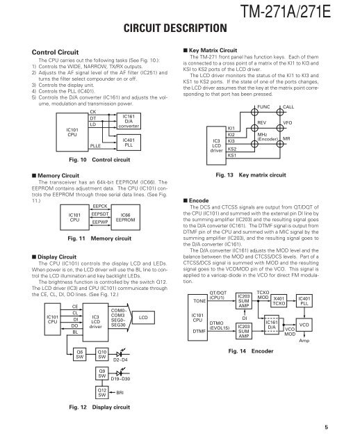
CIRCUIT DESCRIPTION<br />
<strong>TM</strong>-<strong>271A</strong>/271E<br />
Control Circuit<br />
<strong>The</strong> CPU carries out the following tasks (See Fig. 10.):<br />
1) Controls the WIDE, NARROW, TX/RX outputs.<br />
2) Adjusts the AF signal level of the AF filter (IC251) and<br />
turns the filter select compounder on or off.<br />
3) Controls the display unit.<br />
4) Controls the PLL (IC401).<br />
5) Controls the D/A converter (IC161) and adjusts the volume,<br />
modulation and transmission power.<br />
IC101<br />
CPU<br />
CK<br />
DT<br />
LD<br />
PLLE<br />
IC161<br />
D/A<br />
converter<br />
IC401<br />
PLL<br />
■ Memory Circuit<br />
<strong>The</strong> transceiver has an 64k-bit EEPROM (IC66). <strong>The</strong><br />
EEPROM contains adjustment data. <strong>The</strong> CPU (IC101) controls<br />
the EEPROM through three serial data lines. (See Fig.<br />
11.)<br />
EEPCK<br />
IC101<br />
CPU<br />
EEPSDT<br />
EEPWP<br />
IC66<br />
EEPROM<br />
■ Display Circuit<br />
<strong>The</strong> CPU (IC101) controls the display LCD and LEDs.<br />
When power is on, the LCD driver will use the BL line to control<br />
the LCD illumination and key backlight LEDs.<br />
<strong>The</strong> brightness function is controlled by the switch Q12.<br />
<strong>The</strong> LCD driver (IC3) and CPU (IC101) communicate through<br />
the CE, CL, DI, DO lines. (See Fig. 12.)<br />
IC101<br />
CPU<br />
Fig. 10<br />
Fig. 11<br />
CE<br />
CL<br />
DI<br />
DO<br />
BL<br />
Control circuit<br />
Memory circuit<br />
IC3<br />
LCD<br />
driver<br />
COM0~<br />
COM3<br />
SEG0~<br />
SEG30<br />
LCD<br />
■ Key Matrix Circuit<br />
<strong>The</strong> <strong>TM</strong>-271 front panel has function keys. Each of them<br />
is connected to a cross point of a matrix of the KI1 to KI3 and<br />
KSI to KS2 ports of the LCD driver.<br />
<strong>The</strong> LCD driver monitors the status of the KI1 to KI3 and<br />
KS1 to KS2 ports. If the state of one of the ports changes,<br />
the LCD driver assumes that the key at the matrix point corresponding<br />
to that port has been pressed.<br />
IC3<br />
LCD<br />
driver<br />
KI1<br />
KI2<br />
KI3<br />
KS2<br />
KS1<br />
FUNC<br />
REV<br />
MHz<br />
(Encoder)<br />
CALL<br />
VFO<br />
MR<br />
■ Encode<br />
<strong>The</strong> DCS and CTCSS signals are output from QT/DQT of<br />
the CPU (IC101) and summed with the external pin DI line by<br />
the summing amplifier (IC203) and the resulting signal goes<br />
to the D/A converter (IC161). <strong>The</strong> D<strong>TM</strong>F signal is output from<br />
D<strong>TM</strong>F pin of the CPU and summed with a MIC signal by the<br />
summing amplifier (IC203), and the resulting signal goes to<br />
the D/A converter (IC161).<br />
<strong>The</strong> D/A converter (IC161) adjusts the MOD level and the<br />
balance between the MOD and CTCSS/DCS levels. Part of a<br />
CTCSS/DCS signal is summed with MOD and the resulting<br />
signal goes to the VCOMOD pin of the VCO. This signal is<br />
applied to a varicap diode in the VCO for direct FM modulation.<br />
TONE<br />
IC101<br />
CPU<br />
D<strong>TM</strong>F<br />
Fig. 13<br />
QT/DQT<br />
(CPU1)<br />
D<strong>TM</strong>O<br />
(EVOL15)<br />
Key matrix circuit<br />
IC203<br />
SUM<br />
AMP<br />
DI<br />
IC203<br />
SUM<br />
AMP<br />
TCXO<br />
MOD<br />
X401<br />
TCXO<br />
IC161<br />
D/A<br />
VCO<br />
MOD<br />
IC401<br />
PLL<br />
VCO<br />
Amp<br />
Q6<br />
SW<br />
Q10<br />
SW<br />
D2~D4<br />
Fig. 14<br />
Encoder<br />
Q9<br />
SW<br />
D19~D30<br />
Q12<br />
SW<br />
BRI<br />
Fig. 12<br />
Display circuit<br />
5