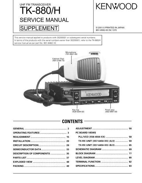
TK-880/H (UHF) mobile service manual - The Repeater Builder's ...
TK-880/H (UHF) mobile service manual - The Repeater Builder's ...
TK-880/H (UHF) mobile service manual - The Repeater Builder's ...

You also want an ePaper? Increase the reach of your titles
YUMPU automatically turns print PDFs into web optimized ePapers that Google loves.
<strong>UHF</strong> FM TRANSCEIVER<br />
<strong>TK</strong>-<strong>880</strong>/H<br />
SERVICE MANUAL<br />
SUPPLEMENT<br />
© 2001-5 PRINTED IN JAPAN<br />
B51-8582-00 (N) 1370<br />
This <strong>service</strong> <strong>manual</strong> applied to products with 30200001 or subsequent serial numbers.<br />
In terms of the products with the serial numbers earier than 30200001, refer to the <strong>TK</strong>-<strong>880</strong>/H<br />
<strong>service</strong> <strong>manual</strong> as per part No. B51-8462-10.<br />
Cabinet (Top)<br />
(A01-2165-13)<br />
Microphone<br />
(T91-0621-05)<br />
Key top<br />
(K29-5284-02)<br />
Panel assy<br />
(A62-0991-03)<br />
CONTENTS<br />
GENERAL ................................................................. 2<br />
OPERATING FEATURES ......................................... 3<br />
REALIGNMENT...................................................... 15<br />
INSTALLATION...................................................... 20<br />
CIRCUIT DESCRIPTION......................................... 28<br />
SEMICONDUCTOR DATA..................................... 33<br />
DESCRIPTION OF COMPONENTS ....................... 35<br />
PARTS LIST ............................................................ 37<br />
EXPLODED VIEW .................................................. 48<br />
PACKING ................................................................ 49<br />
ADJUSTMENT ....................................................... 50<br />
PC BOARD VIEWS<br />
PLL/VCO (X58-4550-XX) .................................. 58<br />
TX-RX UNIT (X57-6450-XX) (A/2) ................... 59<br />
TX-RX UNIT (X57-6450-XX) (B/2).................... 65<br />
SCHEMATIC DIAGRAM ........................................ 69<br />
BLOCK DIAGRAM.................................................. 77<br />
LEVEL DIAGRAM................................................... 80<br />
TERMINAL FUNCTION ......................................... 82<br />
SPECIFICATIONS................................................... 83
<strong>TK</strong>-<strong>880</strong>/H<br />
GENERAL<br />
INTRODUCTION<br />
SCOPE OF THIS MANUAL<br />
This <strong>manual</strong> is intended for use by experienced technicians<br />
familiar with similar types of commercial grade communications<br />
equipment. It contains all required <strong>service</strong> information<br />
for the equipment and is current as of this publication<br />
date. Changes which may occur after publication are<br />
covered by either Service Bulletins or Manual Revisions,<br />
which are issued as required.<br />
ORDERING REPLACEMENT PARTS<br />
When ordering replacement parts or equipment information,<br />
the full part identification number should be included.<br />
This applies to all parts : components, kits, and chassis. If<br />
the part number is not known, include the chassis or kit<br />
number of which it is a part and a sufficient description of<br />
the required component, for proper identification.<br />
PERSONNEL SAFETY<br />
<strong>The</strong> following precautions are recommended for personnel<br />
safety :<br />
• DO NOT transmit if someone is within two feet (0.6<br />
meter) of the antenna.<br />
• DO NOT transmit until all RF connectors are secure and<br />
any open connectors are properly terminated.<br />
• SHUT OFF this equipment when near electrical blasting<br />
caps or while in an explosive atmosphere.<br />
• All equipment should be properly grounded before<br />
power-up for safe operation.<br />
• This equipment should be <strong>service</strong>d by only qualified<br />
technicians.<br />
PRE-INSTALLATION CONSIDERNATIONS<br />
1. UNPACKING<br />
Unpack the radio from its shipping container and check<br />
for accessory items. If any item is missing, please contact<br />
KENWOOD immediately.<br />
2. LICENSING REQUIREMENTS<br />
Federal regulations require a station license for each radio<br />
installation (<strong>mobile</strong> or base) be obtained by the equipment<br />
owner. <strong>The</strong> licensee is responsible for ensuring transmitter<br />
power, frequency, and deviation are within the limits<br />
permitted by the station license.<br />
Transmitter adjustments may be performed only by a licensed<br />
technician holding an FCC first, second or general<br />
class commercial radiotelephone operator’s license. <strong>The</strong>re<br />
is no license required to install or operate the radio.<br />
3. PRE-INSTALLATION CHECKOUT<br />
3-1. Introduction<br />
Each radio is adjusted and tested before shipment. However,<br />
it is recommended that receiver and transmitter operation<br />
be checked for proper operation before installation.<br />
3-2. Testing<br />
<strong>The</strong> radio should be tested complete with all cabling and<br />
accessories as they will be connected in the final installation.<br />
Transmitter frequency, deviation, and power output<br />
should be checked, as should receiver sensitivity, squelch<br />
operation, and audio output. QT equipment operation<br />
should be verified.<br />
4. PLANNING THE INSTALLATION<br />
4-1. General<br />
Inspect the vehicle and determine how and where the<br />
radio antenna and accessories will be mounted.<br />
Plan cable runs for protection against pinching or crushing<br />
wiring, and radio installation to prevent overheating.<br />
4-2. Antenna<br />
<strong>The</strong> favored location for an antenna is in the center of a<br />
large, flat conductive area, usually at the roof center. <strong>The</strong><br />
trunk lid is preferred, bond the trunk lid and vehicle chassis<br />
using ground straps to ensure the lid is at chassis ground.<br />
4-3. Radio<br />
<strong>The</strong> universal mount bracket allows the radio to be<br />
mounted in a variety of ways. Be sure the mounting surface<br />
is adequate to support the radio’s weight. Allow sufficient<br />
space around the radio for air cooling. Position the radio<br />
close enough to the vehicle operator to permit easy access<br />
to the controls when driving.<br />
4-4. DC Power and wiring<br />
1. This radio may be installed in negative ground electrical<br />
systems only. Reverse polarity will cause the cable fuse<br />
to blow. Check the vehicle ground polarity before installation<br />
to prevent wasted time and effort.<br />
2. You must connect the positive power lead directly to<br />
the positive terminal of the vehicle battery. Never<br />
connect the lead to any other positive power source,<br />
such as a cigarette lighter jack or fuse terminals.<br />
CAUTION<br />
If DC power is to be controlled by the vehicle ignition<br />
switch, a switching relay should be used to switch the positive<br />
power lead. <strong>The</strong> vehicle ignition switch then controls<br />
DC to the relay coil.<br />
3. You must also connect the ground lead directly to<br />
the negative terminal of the vehicle battery.<br />
4. <strong>The</strong> cable provided with the radio is sufficient to handle<br />
the maximum radio current demand. If the cable must be<br />
extended, be sure the additional wire is sufficient for the<br />
current to be carried and length of the added lead.<br />
2
GENERAL / OPERATING FEATURES<br />
<strong>TK</strong>-<strong>880</strong>/H<br />
5. INSTALLATION PLANNING – CONTROL STATIONS<br />
5-1. Antenna system<br />
Control station. <strong>The</strong> antenna system selection depends<br />
on many factors and is beyond the scope of this <strong>manual</strong>.<br />
Your KENWOOD dealer can help you select an antenna system<br />
that will best serve your particular needs.<br />
5-2. Radio location<br />
Select a convenient location for your control station radio<br />
which is as close as practical to the antenna cable entry<br />
point. Secondly, use your system’s power supply (which<br />
supplies the voltage and current required for your system).<br />
Make sure sufficient air can flow around the radio and power<br />
supply to allow adequate cooling.<br />
SERVICE<br />
This radio is designed for easy servicing. Refer to the<br />
schematic diagrams, printed circuit board views, and alignment<br />
procedures contained in this <strong>manual</strong>.<br />
Note<br />
When you modify your radio as described in system setup,<br />
take the following precaution.<br />
<strong>The</strong> rating of pin 7 (SB) of the accessory connector cable<br />
(KCT-19) on the rear of the radio is 13.6V (1A). Insert a 1A<br />
fuse if you use the SB pin for external equipment.<br />
13<br />
15<br />
7<br />
6<br />
Accessory connector<br />
cable (KCT-19)<br />
1<br />
3<br />
If you do not intend to use the 3.5-mm jack for the external<br />
speaker, fit the supplied speaker-jack cap (B09-0235-05)<br />
to stop dust and sand getting in.<br />
+<br />
–<br />
1. Operation Features<br />
<strong>The</strong> <strong>TK</strong>-<strong>880</strong>/<strong>880</strong>H is a <strong>UHF</strong> FM radio designed to operate<br />
in both trunking format (LTR model) and conventional format<br />
(Conventional model). <strong>The</strong> programmable features are<br />
summarized.<br />
Model Trunking format Trunking mode<br />
Conventional format<br />
Conventional mode<br />
1-1. Trunking Format<br />
This format can handle up to 32 systems with up to 250<br />
groups in each system. <strong>The</strong> transceiver can be used in both<br />
trunked mode and conventional mode. Systems, groups,<br />
and their functions are programmed.<br />
1-2. Conventional Format<br />
This format can handle up to 250 groups with 250 channels<br />
in each group. <strong>The</strong> transceiver can be used only in conventional<br />
mode. Groups, channels, and their functions are<br />
programmed.<br />
2. Transceiver Controls and Indicators (Fig. 1)<br />
2-1. Front Panel Controls<br />
All the keys on the front panel are momentary-type push<br />
buttons. <strong>The</strong> functions of these keys are explained below.<br />
• POWER key<br />
Transceiver POWER key. When the power is switched<br />
off, all the parameters, such as the system and group in<br />
trunking format, and the group and channel in conventional<br />
format, are stored in memory. When the power is switched<br />
on again, the transceiver returns to the previous conditions.<br />
• SYSTEM UP/DOWN key<br />
(Trunking format, programmable)<br />
• GROUP UP/DOWN key<br />
(Conventional format, programmable)<br />
• SCAN key (Programmable)<br />
• MONITOR key (Programmable)<br />
• A, B, C and D key (Programmable)<br />
• VOLUME UP/DOWN key (Programmable)<br />
Speaker-jack cap<br />
(B09-0235-05)<br />
• BUSY/TX LED<br />
<strong>The</strong> BUSY indicator (Green LED) shows that the channel<br />
is in use. <strong>The</strong> TX indicator (Red LED) shows that you are<br />
transmitting.<br />
3
<strong>TK</strong>-<strong>880</strong>/H<br />
OPERATING FEATURES<br />
2-2. Programmable Keys<br />
<strong>The</strong> FPU (KPG-49D) enables programmable keys to select<br />
the following functions.<br />
■ Conventional format<br />
AUX-A, AUX-B (Only when voice scrambler is not selected),<br />
Channel down, Channel up, DTMF ID (BOT), DTMF<br />
ID (EOT), Display character, Emergency (Only foot key),<br />
Function, Group down, Group up, Home channel, Horn alert,<br />
Key lock, Memory (RCL/STO), Memory (RCL), Memory<br />
(STO), Monitor A, Monitor B, Monitor C, Monitor D, Operator<br />
selectable tone, Public address, Redial, Scan, Scan del/<br />
add, Scrambler (Only when voice scrambler is selected),<br />
Talk around, Volume down, Volume up and None.<br />
■ Trunking format<br />
Auto tel, AUX-A, AUX-B (Only when voice scrambler is<br />
not selected), DTMF ID (BOT), DTMF ID (EOT), Display character,<br />
Emergency (Only foot key), Function, Group down,<br />
Group up, Home group, Horn alert, Key lock, Memory (RCL/<br />
STO), Memory (RCL), Memory (STO), Monitor A, Monitor B,<br />
Monitor C, Monitor D, Public address, Redial, Scan, Scan<br />
del/add, Scan temporary delete, Scrambler (Only when<br />
voice scrambler is selected), System down, System up, TEL<br />
disconnect, Volume down, Volume up and None.<br />
<strong>The</strong>se functions the FPU programs to the function keys<br />
and described in the following sections.<br />
• Auto TEL (Trunking format)<br />
Automatically connects available repeaters that are connected<br />
to telephone circuits when operating as LTR system.<br />
<strong>The</strong> time allocated to search for available repeaters is 60<br />
seconds, after which connection failure occurs, a DTMF<br />
tone is output and the function terminates.<br />
If connection to an available circuit is made, only ID 253,<br />
EOT or hang-up time-out can terminate the function.<br />
• AUX-A<br />
If this key is pressed, “AUX” icon lights on the LCD and<br />
AUX port which is inside of the transceiver turns to the high<br />
level. If pressed again, the “AUX” icon goes off and the<br />
AUX ports turns to the lower level.<br />
• AUX-B<br />
This function can be programmed when the voice scrambler<br />
board is not installed.<br />
If this key is pressed, an underscore (“_”) appears at the<br />
extreme right of the LCD and AUX port which is inside of the<br />
transceiver turns to the active level. If pressed again, the<br />
underscore disappears and the AUX ports turns to the<br />
deactive level.<br />
• Channel up/down (Conventional format)<br />
When the key is pressed each time, the channel number<br />
to be selected is incremented/decremented and repeats if<br />
held for one second or longer. This key works as the voice<br />
scrambler code selector in the voice scrambler code select<br />
mode.<br />
• DTMF ID (BOT)<br />
In conventional mode, if you press this key, a predetermined<br />
DTMF ID (Begin of TX) will be sent automatically.<br />
• DTMF ID (EOT)<br />
In conventional mode, if you press this key, a predetermined<br />
DTMF ID (End of TX) will be sent automatically.<br />
• Display character<br />
This key switches the LCD display between the system<br />
and group number in trunking format and the group and<br />
channel name in conventional format.<br />
• Emergency<br />
Pressing this key for longer than the programmed “Emergency<br />
Key Delay Time” causes the transceiver to enter the<br />
emergency mode. <strong>The</strong> transceiver jumps to the programmed<br />
“Emergency system and group in trunking format<br />
and the group and channel in conventional format” and<br />
transmits for the programmed “Active Time”.<br />
<strong>The</strong> transceiver disables mic mute while transmitting.<br />
After finishing transmission, the transceiver receivers for<br />
the programmed “Interval Time”. <strong>The</strong> transceiver mutes<br />
the speaker while receiving. Following the above sequence,<br />
the transceiver continues to transmit and receive.<br />
• Function<br />
Pressing this key causes the transceiver to display<br />
“FCN”. <strong>The</strong>n, pressing a microphone DTMF key causes the<br />
corresponding programmed function to start. This key may<br />
be convenient when using many functions with the microphone<br />
12-key keypad.<br />
• Group up/down<br />
When the key is pressed each time, the group number to<br />
be selected is incremented/decremented and repeats if held<br />
for one second or longer.<br />
• Home channel (Conventional format)<br />
Press this key once, the channel switches to the pre-programmed<br />
home channel.<br />
• Home group (Trunking format)<br />
Each pressing of the key selects a preset system/group.<br />
• Horn alert<br />
If you are called from the base station using 2-tone/DTMF<br />
while you are away from your transceiver, you will be<br />
alerted by the vehicle horn or some other type of external<br />
alert. To turn the horn alert function on , press this key. A<br />
confirmation tone sounds, and the display shows “HA” on<br />
the sub LCD.<br />
If this key is pressed again, the horn alert function is<br />
turned off.<br />
• Key lock<br />
Pressing this key causes the transceiver to accept entry<br />
of only the [Function], [Key lock], [PTT], [Monitor A], [Monitor<br />
B], [Monitor C], [Monitor D], and [Emergency] keys.<br />
4
OPERATING FEATURES<br />
<strong>TK</strong>-<strong>880</strong>/H<br />
• Message mode<br />
Press this key to enter the message mode. (See “Alphanumeric<br />
Two-way Paging Function” for details)<br />
• Memory<br />
This key allows DTMF memory data to be recalled; up to<br />
32 memories each with a memory dial of up to 16 digits and<br />
an A/N of up to 10 digits per memory.<br />
• Monitor<br />
Used to release signalling or squelch when operating as a<br />
conventional. It is also used to reset option signalling.<br />
• Operator selectable tone (Conventional format)<br />
This key switches the pre-set decode QT/DQT and encode<br />
QT/DQT to OST (Operator Selectable Tone) tone pair.<br />
Press this key, the transceiver enters to OST select<br />
mode. In this mode, the display shows “OFF” and the operator<br />
can select one of the OST tone pair using the group<br />
up/down key. <strong>The</strong> display shows “TONE ” and tone<br />
**<br />
pair No. is selected.<br />
**<br />
Press OST key again, the transceiver exits from the OST<br />
select mode, and returns to the group/channel mode with<br />
the handset indicator ( ). <strong>The</strong> handset indicator ( ) means<br />
that the OST tone pair is selected. OST tone pair number or<br />
OFF can be memorized for each channel.<br />
16 kinds of tone pair for OST can be programmed by<br />
KPG-49D. OST is useful to access the repeater with same<br />
radio frequency and different tone (QT/DQT).<br />
• Public address<br />
Public address amplifies the microphone audio, and outputs<br />
it through a PA speaker. PA is activated by pressing<br />
this key. A confirmation tone sounds, and the display shows<br />
“PUBLIC ADRS”. PA can be activated at anytime (scanning<br />
or non-scanning).<br />
<strong>The</strong> RADIO continues to scan & receive calls while in PA<br />
mode. Pressing PTT activates PA, and will override an incoming<br />
call at anytime; however, no RADIO transmission<br />
takes place.<br />
If this key is pressed again, a confirmation tone will<br />
sound, the display will return to the normal channel or SCAN<br />
display, and the PA function will turn off.<br />
• Redial<br />
If you press this key when the system/group (Trunking<br />
format) or group/channel (Conventional format) is displayed,<br />
the last transmitted DTMF code will appear on the display.<br />
Pressing the PTT switch at this time will transmit the displayed<br />
DTMF code.<br />
• Scan<br />
Press this key starts scanning. Pressing this key stops<br />
scanning.<br />
• Scan del/add<br />
1) Trunking format<br />
Used to select whether system scan routines are used<br />
during system scan. Each pressing of the key (to ON)<br />
toggles between lockout and lock. <strong>The</strong> scan routine is<br />
started when on lock. <strong>The</strong> DEL indicator flashes when the<br />
system is on lockout.<br />
2) Conventional format<br />
This key switches the currently displayed channel between<br />
“Delete” and “Add”.<br />
<strong>The</strong> “Add” channel contained in the scan sequence, and<br />
“Delete” channel is not contained. In the scan mode, this<br />
key switches the channnel delete or add temporarily.<br />
• Scan temporary delete (Trunking format)<br />
This key is temporarily deleted a system being scanned.<br />
If you press this key when scan is stopped (when a call is<br />
being received from another station), the system is temporarily<br />
deleted and scanning restarts.<br />
This key operates even when “Scan Type” is set to “List<br />
Type System Scan”.<br />
• Scrambler<br />
If a scrambler code (1 to 16) has been set in the FPU, an<br />
underscore (“_”) appears at the extreme right of the LCD<br />
display when scrambler is active. Pressing this key changes<br />
on/off of scramble operation. Press this key for 2 seconds<br />
to enter scrambler code selection mode.<br />
• Send GPS (Optional)<br />
Pressing this key causes the transceiver to send a single<br />
GPS data. (GPS receiver must be installed.)<br />
• System up/down (Trunking format)<br />
When the key is pressed each time, the system number<br />
to be selected is incremented/decremented and repeats if<br />
held for one second or longer.<br />
• Talk around (Conventional format)<br />
Press this key, the transceiver uses the receive frequency<br />
and the tone for transmission.<br />
<strong>The</strong> operator can call the other party directory (without<br />
repeater). Press this key again, the talk around function<br />
goes off.<br />
• Telephone disconnect (Trunking format)<br />
Pressing this key ends an RIC connection (disconnects<br />
the telephone line).<br />
• Volume up/down<br />
When the key is pressed, the volume level is increased/<br />
decreased and repeats if held for 200ms or longer.<br />
• None<br />
Sounds error operation beep, and no action will occur.<br />
Use this function when the transceiver is required to be<br />
more simple operated.<br />
5
<strong>TK</strong>-<strong>880</strong>/H<br />
OPERATING FEATURES<br />
2-3. Front Panel Displays and Indicators<br />
1 Sub display<br />
Displays the system, channel and group numbers. Also<br />
displays various functions, such as TA.<br />
2 P (Priority) indicator<br />
<strong>The</strong> P indicator ( ) appears when a selected channel is<br />
programmed as priority, in conventional operation.<br />
3 MON (Monitor) indicator<br />
<strong>The</strong> MON indicator appears when the button programmed<br />
as MONITOR is pressed.<br />
4 SVC (Service) indictor<br />
This icon is not used this transceiver.<br />
5 SCN (Scan) indicator<br />
<strong>The</strong> SCN indicator appears when using scan mode.<br />
6 AUX (Auxiliary) indicator<br />
appears when the auxiliary function is activated (ON) by<br />
pressing the AUX-A key.<br />
7 Handset indicator<br />
<strong>The</strong> handset indicator ( ) appears when the selected<br />
group is programmed as telephone IDs (Trunking format).<br />
In conventional format, the handset indicator ( ) appears<br />
when the OST tone pair is selected.<br />
8 MAIL indicator<br />
Flashes when a status message (FleetSync) is received.<br />
Lights when a status message is stored in the stack<br />
memory.<br />
9 Alphanumeric display<br />
<strong>The</strong> twelve-character dot matrix alphanumeric display<br />
shows the system/group numbers. You can program system/group<br />
names with up to ten characters in place of these<br />
numbers. <strong>The</strong> left display is used as a delete indicator ( )<br />
and the right is used for the selective call ( ) or scrambler<br />
(_) function. <strong>The</strong> delete indicator shows<br />
*<br />
the systems<br />
locked out of the scanning sequence. Selective call and<br />
scrambler are optional functions that can be programmed.<br />
Dispalys received messages when using FleetSync.<br />
10 A,B,C,D key<br />
<strong>The</strong>se keys are programmable function (PF) keys.<br />
BUSY/ VOLUME<br />
TX LED UP<br />
VOLUME<br />
POWER DOWN<br />
1 2 3<br />
4 5 6 7 8<br />
SYSTEM UP<br />
(Trunking Format)<br />
GROUP UP<br />
(Conventional Format)<br />
SYSTEM DOWN<br />
(Trunking Format)<br />
GROUP DOWN<br />
(Conventional Format)<br />
MODULAR<br />
MIC JACK<br />
MONITOR<br />
10 9<br />
SCAN<br />
Fig. 1<br />
3. Scan Operating<br />
3-1. Trunking Format<br />
■ System scan<br />
System scan can be selected with the “Scan” key by programming<br />
the scan feature. When the “Scan” key is<br />
pressed and the “SCN” mark appears, scan mode in entered.<br />
Scanning starts from the system following the currently<br />
displayed system. When a call is received, scanning<br />
stops, and the system and group are displayed.<br />
When programming key is touched during scanning, the<br />
scan stops and the revert system or group can be changed.<br />
Scanning resumes one second after the key is released.<br />
<strong>The</strong>re are two types of system scan.<br />
• Fix system scan<br />
All the set systems except locked-out ones are scanned.<br />
If the Del/Add feature is assigned to the programmable key,<br />
it can be controlled from the front panel.<br />
• List type system scan<br />
A scan list can be set for each system.<br />
<strong>The</strong> list to be scanned can be changed by changing the<br />
display system.<br />
If many systems have been set, the scan speed can be<br />
increased by narrowing the systems to be scanned with<br />
scan lists.<br />
6
OPERATING FEATURES<br />
<strong>TK</strong>-<strong>880</strong>/H<br />
■ System lockout<br />
<strong>The</strong> system lockout feature is used to lock systems out<br />
of the scan sequence, and can be selected by programming<br />
in the following two ways;<br />
• Fixed lockout<br />
<strong>The</strong> system to be locked out is selected by programming.<br />
When a locked system is selected, the Delete ( ) indicator<br />
appears on the left of the SYSTEM indicator. <strong>The</strong> revert system<br />
is scanned even if it is locked out. If there is a locked<br />
system, the Delete ( ) indicator flashes during fixed scanning.<br />
• User selectable lockout<br />
If the scan lockout feature is programmed to a key, the<br />
user can lock systems out of the scan sequence with the<br />
key. To lock a system out of the scan sequence, press the<br />
key when the system is displayed. <strong>The</strong> Delete ( ) indicator<br />
is displayed on the left of the SYSTEM indicator.<br />
To unlock a system, select the system and press the key.<br />
<strong>The</strong> Delete ( ) indicator disappears to indicate that the system<br />
has returned to the scan sequence. <strong>The</strong> revert system<br />
is scanned even if it is locked out. If there a locked system,<br />
the Delete ( ) indicator flashes during fixed scanning. If all<br />
systems are locked out, the scan stops and only the revert<br />
system is received.<br />
■ Drop-out delay time (Scan resume time)<br />
If a call is received during scan, the scan stops. <strong>The</strong> scan<br />
resume time can be programmed as 0 to 300 seconds in<br />
one-second increments. <strong>The</strong> default value is 3 seconds.<br />
■ Dwell time<br />
<strong>The</strong> dwell time is the time after transmission ends until<br />
the scan resumes in scan mode. It can be set 0 to 300 seconds<br />
by programming. <strong>The</strong> default value is 3 seconds.<br />
■ System/group revert<br />
System/group revert can be programmed for one of the<br />
following;<br />
• Last called revert<br />
<strong>The</strong> system or group changes to the revert system or<br />
group when a call is received with the system or group being<br />
scanned.<br />
• Last used revert<br />
If a system/group call is received during scanning and the<br />
PTT button is pressed for transmission and response within<br />
the drop out delay time, the system or group is assigned as<br />
the new revert system or group.<br />
• Selected revert<br />
If the system/group was changed while scanning, the<br />
newly selected system/group.<br />
• Selected + Talkback revert<br />
If the system/group was changed while scanning, the<br />
newly selected system/group. <strong>The</strong> transceiver “talks back”<br />
on the current receive group.<br />
■ Scan massage wait<br />
<strong>The</strong> time for staying with the home repeater that receives<br />
a signal during system scan and monitoring data<br />
messages can be programmed. If there is no signal from<br />
the home repeater, the system is scanned for about 50ms.<br />
If there is a signal, three data messages are monitored.<br />
Normally, three data messages are monitored for each system,<br />
and it can be increased in multiples of three data messages<br />
per line to up to eight lines.<br />
If the repeater data message indicates that there is no<br />
call, data monitoring is terminated and the home repeater of<br />
the next system is scanned.<br />
■ Group scan operation<br />
Group scan can be programmed for each group. In addition<br />
to the ID codes of the selected group, the ID codes of<br />
the other groups that are permitted for group scan are decoded.<br />
(<strong>The</strong> two fixed ID and block decode codes are always<br />
decoded.)<br />
If, during group scanning, a call is received with one of<br />
the selectable group ID codes for which group scan is enabled,<br />
the group display indicates the group number that the<br />
call came in with. That group then becomes the new selected<br />
group. Group scan resumes after the specified dropout<br />
delay time or dwell time shared by the system scan<br />
elapses.<br />
■ In conventional system<br />
If QT or DQT is set for the channel, the channels, including<br />
signalling, are scanned.<br />
In case of the priority group is set in conventional system,<br />
if a group scan (including group scan during a system<br />
scan) temporarily stops (receiving) in a group that does not<br />
have priority, a look back is performed to the priority group.<br />
Look back is performed according to the look back time A<br />
and B settings. If a call is received on the priority group,<br />
reception immediately switches to the priority group.<br />
3-2. Conventional Format<br />
■ Scan types<br />
• Single group scan<br />
You can scan all valid (ADD) channels in the displayed<br />
group that can be selected with the group up/down key.<br />
• Multiple group scan<br />
You can scan all valid (ADD) channels in the all valid<br />
(ADD) group.<br />
7
<strong>TK</strong>-<strong>880</strong>/H<br />
OPERATING FEATURES<br />
■ SCAN start condition<br />
One or more non-priority channels must be added to all<br />
channels that can be scanned. <strong>The</strong> transceiver must be in<br />
normal receive mode (PTT off).<br />
When you activate the key programmed to the scan function,<br />
the scan starts. <strong>The</strong> scan icon “SCN” lights and “–<br />
SCAN–” or revert channel (programmable) is indicated on<br />
alphanumeric display.<br />
■ Scan stop condition<br />
<strong>The</strong> scan stops temporarily if the following conditions are<br />
satisfied.<br />
1) A carrier is detected, then signalling matches on channels<br />
for which receive the signalling is set by the programming<br />
software.<br />
2) A carrier is detected on the channels for which receiving<br />
signalling is not set by the programming software or<br />
when the monitor (signalling cancel) function is activated.<br />
■ Scan channel types<br />
1) Priority channel is the most important channel for the<br />
scan, and always detects a signal during scan and when<br />
the scan stops temporarily.<br />
2) Non-priority channels detects a signal during scan. For<br />
the channels that can be selected with the group or channel<br />
up/down key when the scan does not occur, adds an<br />
indicator “▼” lights.<br />
■ Priority channel setting<br />
A priority channel can be set as follows with the programming<br />
software (KPG-49D).<br />
1) Specify a priority channel as a fixed priority channel.<br />
2) Make a selected channel, a priority channel.<br />
■ Scan type according to the priority channel<br />
1) When no priority channel is set : Only the non-priority<br />
channels are scanned.<br />
If a non-priority channel stops temporarily, it stops until<br />
there is no signal on the channel.<br />
2) When priority channel is set : Either priority channel is<br />
scanned.<br />
If a non-priority channel stops temporarily, a priority channel<br />
signal is detected at certain intervals.<br />
If a priority channel stops temporarily, it stops until there<br />
is no signal on the priority channel.<br />
■ Revert channel<br />
<strong>The</strong> revert channel is used to transmit during scanning<br />
and set by the programming software (KPG-49D).<br />
1) Priority<br />
<strong>The</strong> transceiver reverts to the priority channel.<br />
2) Priority + talkback<br />
<strong>The</strong> transceiver reverts to the priority channel.<br />
If you press PTT during a resume timer (dropout delay<br />
time, TX dwell time) or calling, you can transmit on current<br />
channel to answer to the call however revert channel<br />
is set to priority channel.<br />
After resume time, scan re-starts and transmission channel<br />
is return to priority channel.<br />
3) Selected channel<br />
<strong>The</strong> transceiver reverts to the channel before scanning or<br />
the channel that you changed during scan.<br />
4) Last called channel<br />
<strong>The</strong> transceiver reverts to the last called channel during<br />
the scan.<br />
5) Last used channel<br />
<strong>The</strong> transceiver reverts to the last used (transmitted)<br />
channel during scan. “Last used” revert channel includes<br />
talkback function.<br />
6) Selected + talkback<br />
<strong>The</strong> transceiver reverts to the channel before scanning or<br />
the channel that you changed during scan.<br />
■ Scan end<br />
When you reactivate the key programmed to the scan<br />
function during scan mode, the scan ends.<br />
<strong>The</strong> scan icon “SCN” and “–SCAN–” or revert channel<br />
(programmable) display goes off.<br />
■ Temporarily delete/add<br />
It is possible to delete or add channel temporarily during<br />
scan. When scan stops on unnecessary channel for example<br />
by interference of the other party, activate the delete/<br />
add function (for example press the key), then that channel<br />
is deleted temporarily and scan re-start immediately.<br />
When you would like to add the deleted channel temporarily<br />
to scan sequence, select the desired (deleted) channel<br />
during scan, activate the delete/add function (for example<br />
press the key) before scan re-start.<br />
That channel is added temporarily to scan sequence. <strong>The</strong><br />
temporary deleted or added channels are returns to pre-set<br />
delete/add, when the transceiver exits from scan mode.<br />
4. Details of Features<br />
4-1. Common Trunking format and Conventional Format<br />
■ Time-out timer<br />
<strong>The</strong> time-out timer can be programmed in 15 seconds<br />
increments from 15 seconds to 10 minutes. If the transmitter<br />
is keyed continuously for longer than the programmed<br />
time, the transmitter is disabled and a warning tone sounds<br />
while the PTT button is held down. <strong>The</strong> alert tone stops<br />
when the PTT button is released.<br />
8
OPERATING FEATURES<br />
<strong>TK</strong>-<strong>880</strong>/H<br />
■ Sub LCD display<br />
You can use 3-digit the display to display the system<br />
number, channel number or group number. It is useful<br />
when the main (12-digit) display indicates system, group or<br />
channel name or other functions.<br />
■ Selective call alert LED<br />
You can select whether or not the LED on the transceiver<br />
flashes in an orange color when selective call was occurred.<br />
■ PTT ID<br />
PTT ID provides a DTMF or MSK (FleetSync : Fleet-ID)<br />
ANI to be sent with every time PTT (beginning of transmission,<br />
end of transmission, or both).<br />
You can program PTT ID for each group. You can program<br />
a PTT ID as “on” or “off” when “DTMF” is selected<br />
for the PTT ID type. You can program a PTT ID as “own”,<br />
“sel” or “off” when “MSK” is selected for the PTT ID type.<br />
<strong>The</strong> contents of ID are programmed for each transceiver.<br />
<strong>The</strong> timing that the transceiver sends ID is programmable.<br />
BOT : DTMF ID (BOT)/MSK ID is sent on beginning of<br />
transmission.<br />
EOT : DTMF ID (EOT)/MSK ID is sent on end of transmission.<br />
Both : DTMF ID (BOT)/MSK ID is sent on beginning of<br />
transmission and DTMF ID (EOT)/MSK ID is sent on end<br />
of transmission.<br />
■ Radio password<br />
When the password is set in the transceiver, user can not<br />
use the transceiver unless enter the correct password.<br />
This code can be up to 6 digits from 0 to 9 and input with<br />
the key, and "S" key.<br />
■ Off hook decode<br />
If the Off hook decode function has been enabled, removing<br />
and replacing the microphone on the hook has no<br />
effect for decoding QT/DQT and option signalling.<br />
■ Timed power off<br />
This function works as “Automatic Power Switch Off”.<br />
Timed power off timer starts from the ignition-off. After<br />
the timer expires, the radio will automatically turn off. <strong>The</strong><br />
timer will be reset if the ignition is turned on and off.<br />
This function requires ignition-sense. Connect the ignition-line<br />
to the 9-pin connector which is located at the rear of<br />
the radio.<br />
After the timer expires, press the power switch to turn<br />
on the radio.<br />
■ Horn alert<br />
In trunking format, horn alert can be set to on or off for<br />
each group. If horn alert has been set to YES for a group and<br />
DEC ID/QT/DQT matches, the horn alert, HOR. is turned on<br />
and off. <strong>The</strong> group for which the optional signalling is set<br />
works by ANDing the decode ID/QT/DQT with the optional<br />
signalling.<br />
In conventional format, if you are called from the base<br />
station using 2-tone/DTMF while you are away from your<br />
transceiver, you will be alerted by the vehicle horn or some<br />
other type of external alert. To turn horn alert function on,<br />
press the [Horn Alert] key.<br />
Either continuous or non-continuous operation can be set<br />
by the FPU. <strong>The</strong> horn alert port is enabled or disabled as<br />
follows;<br />
Off hook horn alert Hook off Hook on<br />
Enable Yes Yes<br />
Disable No Yes<br />
■ Pulse<br />
<strong>The</strong> horn alert port, HOR, is turned on and off as follows;<br />
0.5s 0.5s 0.5s 0.5s 0.5s<br />
<strong>The</strong> timing when the fixed LTR ID matches is as follows<br />
(trunking format);<br />
1s 0.5s 1s<br />
HOR<br />
■ Continuous<br />
Horn alert can be reset by setting an expiration time from<br />
the FPU, pressing the AUX-A key, or setting off hook.<br />
■ Data TX with QT/DQT<br />
Whether programmed QT/DQT is modulated or not with<br />
a data transmission except for Selcall. A radio unit can receive<br />
a data message regardless of QT/DQT if the receiving<br />
unit is not scanning.<br />
9
<strong>TK</strong>-<strong>880</strong>/H<br />
OPERATING FEATURES<br />
4-2. Trunking Format<br />
■ Call indicator<br />
<strong>The</strong> call indicator can be programmed for each group. In<br />
trunked system, it can be set to respond to a selectable decode<br />
ID or one of two fixed IDs, except block IDs. When a<br />
call is received with a selectable decode ID, the call indicator<br />
flashes. When a call is received with a fixed ID, the call<br />
indicator lights continuously.<br />
On a conventional system, the call indicator can be programmed<br />
to light for each QT or DQT code. It keeps flashing<br />
while a call is being received. It is turned off by pressing<br />
any front panel key.<br />
■ Free system ringback<br />
This feature is available only when a telephone interconnected<br />
ID code is selected. If a busy tone sounds when the<br />
PTT button is pressed, the transceiver enters this mode automatically.<br />
When the PTT button is released, a beep sounds for<br />
400ms to indicate that the mode has been entered. If the<br />
scan is on, it is resumed (the "SCN" mark goes on). When<br />
any repeater becomes available, a ringing tone sounds and<br />
this mode ends.<br />
<strong>The</strong> mode is terminated when the system, group, scan,<br />
PTT, key is changed.<br />
■ System search<br />
This feature can be programmed to automatically access<br />
other programmed systems when the selected system cannot<br />
be accessed. If an intercept tone sounds when the PTT<br />
button is pressed after setting the mode, the transceiver<br />
has entered the mode.<br />
If the group ID is a telephone interconnect ID, the transceiver<br />
then attempts to access, in succession, other systems<br />
that have a telephone interconnect ID in the revert<br />
group location. If the group ID is a dispatch ID, the transceiver<br />
attempts to access other systems that have a dispatch<br />
ID programmed in the revert group location.<br />
If there is no system to be accessed, an intercept tone<br />
sounds, the mode is terminated, and the transceiver returns<br />
to the first system. If the access is successful, the mode is<br />
terminated, and the searched system becomes the new selected<br />
system (If during scanning, the scan stops).<br />
■ Transpond<br />
This feature can be programmed to turn on and off for<br />
each group. If the ID of the group for which transpond is<br />
enabled is received, two data messages (transmit ID and<br />
turn-off code) are automatically transmitted if the PTT button<br />
is not pressed as a response within the time set (0 to<br />
300 seconds in 1-second increments). If the PTT button is<br />
pressed within the time, the transpond is not preformed.<br />
■ Transmit inhibit<br />
<strong>The</strong> transceiver can be programmed with a transmit inhibit<br />
block of ID codes. If an ID code within this block is<br />
decoded the preset time before the PTT button is pressed,<br />
transmission is inhibited. <strong>The</strong> BUSY indicator lights and a<br />
busy tone sounds until the PTT button is released to indicate<br />
that transmission is not possible (except clear-to talk mode).<br />
Transmission with the group for which the encode ID is<br />
not set is inhibited, and the busy tone is output while the<br />
PTT button is held down, regardless of the clear-to talk setting.<br />
■ Auto TEL<br />
A telephone interconnect call can be made by simply<br />
pressing the key by assigning this feature to the key. This<br />
feature accesses the TEL channel of the available system<br />
automatically.<br />
When the key is pressed, a queue tone is output, and the<br />
“AUTO TEL” appears on the alphanumeric display along<br />
with a flashing handset indicator ( ) to indicate that this<br />
mode has been entered. If the TEL ID is set for the revert<br />
system, the TEL channel of that system is accessed. If all<br />
TEL channels are busy, an attempt is made to access the<br />
TEL channels of another system in which the TEL ID code<br />
has been programmed. It is repeated for 60 seconds until<br />
the access succeeds. If the access succeeds, a dial tone<br />
returns from the repeater. If the key is pressed again when<br />
the queue tone is sounding, this mode is canceled.<br />
If the access fails after 60 seconds, a deny tone is output<br />
and this mode is terminated. When the talk ends, the revert<br />
system/group returns. When the scan mode is effective,<br />
the scan resumes. <strong>The</strong> Auto TEL feature can be programmed<br />
to turn on or off for each system.<br />
■ ARQ mode<br />
It affects Trunking mode only. Automatic Repeat<br />
reQuest (ARQ) mode is a manner to minimize the air traffic<br />
of data communication. Also, it enables to occupy the<br />
trunking repeater channel fot the data communication period.<br />
4-3. Conventional Format<br />
■ “TOT” pre-alert<br />
<strong>The</strong> transceiver has “TOT” pre-alert timer. This parameter<br />
selects the time at which the transceiver generates<br />
“TOT” pre-alert tone before “TOT” is expired.<br />
“TOT” will be expired when the selected time passes<br />
from a TOT pre-alert tone.<br />
■ “TOT” re-key time<br />
<strong>The</strong> transceiver has “TOT” re-key timer. This timer is the<br />
time you can not transmit after “TOT” exceeded. After<br />
“TOT” re-key time expired you can transmit again.<br />
10
OPERATING FEATURES<br />
<strong>TK</strong>-<strong>880</strong>/H<br />
■ “TOT” reset time<br />
<strong>The</strong> transceiver has “TOT” reset timer. This timer is the<br />
minimum wait time allowed during a transmission that will<br />
reset the “TOT” count.<br />
“TOT” reset time causes the “TOT” to continue even<br />
after PTT is released unless the “TOT” reset timer has expired.<br />
■ OST (Operator Selectable Tone)<br />
<strong>The</strong> transceiver is capable to have “OST” function and 16<br />
tone pair (QT/DQT) with max 10-digit name for each tone<br />
pair.<br />
■ “OST” back up<br />
<strong>The</strong> transceiver is programmable the selected “OST”<br />
code is memorized or not. If you set to Disable (no memorized),<br />
the “OST” function always starts at “off”.<br />
■ Direct “OST”<br />
It is possible to call “OST” number directory using keypad.<br />
In this case, keypad is used for “OST”, then auto<br />
“PTT” store and send functions by keypad are not usable.<br />
■ Clear to transpond<br />
<strong>The</strong> transceiver waits the transpond of 2-tone /DTMF if<br />
channel is busy until channel open. This feature prevents<br />
the interference to other party.<br />
5. Option Signalling<br />
5-1. DTMF/2-Tone<br />
Built-in DTMF decoder is available for option signalling.<br />
Built-in 2-tone decoder is available for option signalling.<br />
It is possible to use individual call, group call, D.B.D.<br />
(Dead Beat Disable). D.B.D. is used with DTMF only.<br />
If the option signalling matches, a predetermined action<br />
will occur.<br />
If option signalling matches on a group/channel which is<br />
set up with option signalling, the option signalling indicator<br />
( ) will flash and option signalling will be released. <strong>The</strong><br />
*<br />
transpond or alert tone will sound.<br />
If the selective call alert LED is set up, the orange LED<br />
will flash.<br />
While option signalling matches (or if option signalling is<br />
deactivated when you are transmitting), you can mute or<br />
unmute ID/QT/DQT/Carrier.<br />
■ AND/OR<br />
You can select AND or OR for option signalling match<br />
conditions.<br />
Alert/Transpond<br />
AND QT/DQT/ID+DTMF (2-tone); Option matches = Action<br />
OR QT/DQT/ID+DTMF (2-tone); Option matches = Action<br />
AF mute open<br />
AND QT/DQT/ID+DTMF (2-tone); Option matches = Action<br />
OR QT/DQT/ID; Signalling only matches = Action<br />
With OR set up, alert/transpond will not function with<br />
only DTMF (Trunking format).<br />
With OR set up, AF mute will not release when only<br />
DTMF matches.<br />
With a conventional channel not set up with QT or DQT,<br />
only the carrier is considered when signalling matches.<br />
■ Auto Reset<br />
If option signalling matches a group set up with option<br />
signalling, option signalling is released. After matching option<br />
signalling, option signalling will temporarily reset automatically.<br />
■ Dead Beat Disable<br />
If the D.B.D. code matches, a predetermined action will<br />
occur. Whether option signalling is activated or not, when<br />
D.B.D. matches on any channel, the transceiver will become<br />
TX inhibited or TX/RX inhibited. While D.B.D. is active, if the<br />
D.B.D. code + “#” code is received, D.B.D. will disactivate.<br />
When D.B.D. matches, transpond will function. Alert will<br />
not be output, and option signalling match icon will not appear.<br />
5-2. MSK<br />
Built-in MSK (FleetSync : Fleet-ID) decoder is available<br />
for option signalling. When the group ID/Carrier matches,<br />
squelch remains muted while the station waits for reception<br />
of proper MSK signal. When MSK signal matches, squelch<br />
unmutes.<br />
■ AND/OR<br />
AND : QT/DQT/ID + MSK to unmute. MSK matches =<br />
alert tone<br />
OR : QT/DQT/ID to unmute. MSK matches = alert tone<br />
6. Alphanumeric Two-way Paging Function<br />
(FleetSync)<br />
■ General<br />
<strong>The</strong> Alphanumeric Two-way Paging Function<br />
(FleetSync) is a KENWOOD proprietary protocol. It enables<br />
a variety of paging functions.<br />
■ ID Construction<br />
A radio unit ID is defined by a combination of 3-digit Fleet<br />
and 4-digit ID numbers. Each radio unit must be assigned its<br />
own Fleet and ID numbers.<br />
■ PTT ID<br />
A pre-programmed unique ID (own) can be sent at the<br />
beginning of transmission and/or the end of transmission to<br />
identify which radio unit is on air.<br />
When selecting (sel) for MSK ID, the radio calls the specific<br />
Fleet user the same as selective call.<br />
11
<strong>TK</strong>-<strong>880</strong>/H<br />
OPERATING FEATURES<br />
■ Selective Call (SELCALL)<br />
This is a voice call to a particular individual or group of<br />
stations.<br />
• Example of call types;<br />
[100][ALL ] : <br />
All the units whose fleet number is “100” are called.<br />
[100][1000] : <br />
<strong>The</strong> unit, whose the fleet number is “100” and ID number<br />
is “1000”, is called.<br />
[ALL][ALL ] : <br />
All the units are called.<br />
[ALL][1000] : <br />
All ID “1000” are called regardless of their fleet number.<br />
• Unit ID encode block<br />
Encode ID Block can be set to limit <strong>manual</strong> dial ID. <strong>The</strong><br />
radio unit will not accept an ID other than these IDs which<br />
are entered from the keypad. If Inter-fleet Call is enabled,<br />
block ID setting affects each fleet group.<br />
■ Status Message<br />
Using a 2-digit number, you can send and receive a Status<br />
message which may be decided in your talk group. Each<br />
Status may be displayed with 16 alphanumeric characters if<br />
programmed in the radio. A maximum of 9 received messages<br />
can be stored in the stack memory, and it can be reviewed<br />
after reception. If the message memory becomes<br />
full, the oldest one will be erased. <strong>The</strong> stack memory will be<br />
cleared by turning radio power off.<br />
• Status 80~99 (Special)<br />
Status numbers from 80 to 99 are reserved for special<br />
purposes. Entering these statuses from the DTMF keypad<br />
can be inhibited.<br />
Please notice that the following status numbers are used<br />
for special purposes;<br />
80~87 : Reserved for future use.<br />
88 : Terminates to emergency mode.<br />
89 : Request for horn alert.<br />
90 : Remote stun on. Disable the received radio unit’s<br />
TX.<br />
91 : Remote stun on. Disable the received radio unit’s<br />
TX/RX.<br />
92 : Cancel remote stun. Enable the received radio unit’s<br />
TX/RX.<br />
93 : Acknowledgement status sent when the radio unit is<br />
in stun mode (TX disabled).<br />
94 : Acknowledgement status sent when the radio unit is<br />
in stun mode (TX/RX disabled).<br />
95~97 : Reserved for future use.<br />
98 : Man down emergency status (For portable).<br />
99 : Emergency status.<br />
Note : Remote stun works with DTMF D.B.D. function also.<br />
12<br />
• Automatic status response<br />
If you pre-select a status number and leave the radio in<br />
the Status Mode, it can automatically respond with the selected<br />
status number upon request from the base station.<br />
(<strong>The</strong> request function is initiated by serial control on the<br />
base station (Optional).)<br />
■ Short Messase (Optional)<br />
A maximum of 48 characters can be sent (External equipment<br />
is required). Received Short Messages will be displayed<br />
in the same manner as a Status Message. A maximum<br />
of 4 received messages can be stored in the stack<br />
memory. In the Stack Mode, 3-digit LCD indicates the received<br />
Short Message as “M01”~”M04".<br />
■ Long Message (Optional)<br />
A maximum of 1024 characters can be sent (External<br />
equipment is required). Received Long Message will not be<br />
displayed or stacked in the radio memory but is output<br />
through the COM (Data) port.<br />
■ Emergency Function<br />
Emergency status 99 will be sent at the beginning of<br />
each emergency transmission.<br />
• Emergency status response<br />
Either “Horn” or “Alert” can be selected for the called<br />
radio unit’s response to reception of status 99 which is used<br />
as an emergency status.<br />
■ Other Functions<br />
• Manual dial<br />
Fleet, ID and Status numbers can be entered from DTMF<br />
keypad. (DTMF microphopne is required.)<br />
• FleetSync baud rate<br />
MSK data baud rate setting. <strong>The</strong> same rate must be set<br />
as a communication partner.<br />
1200bps :<br />
Data communication is made in 1200bps. <strong>The</strong> communication<br />
area is much wider than 2400bps. Recommended<br />
for repeater operation.<br />
2400bps :<br />
Data communication is made in 2400bps. <strong>The</strong> communication<br />
area is narrower than 1200bps, but it will decrease<br />
the data traffic. Data rate 2400bps may not work properly<br />
depending on the repeater’s characteristic.<br />
• Message mode timer<br />
Message Mode Timer is a delay timer returning from<br />
message/stack mode to Normal mode.<br />
• Status/short/long message on data group/channel<br />
Status/Short/Long Message transmission is made<br />
whether on the Data System/Group in trunking format and<br />
on the Data Group/Channel in conventional format.
OPERATING FEATURES<br />
<strong>TK</strong>-<strong>880</strong>/H<br />
• Status/short/unit ID message serial output<br />
(Option)<br />
Whether a received Status/Short message or PTT ID is<br />
output or not from serial port.<br />
• Caller ID display<br />
PTT ID is displayed on LCD.<br />
• Call alert (Continuous)<br />
<strong>The</strong> radio can provide the alert tone repeatedly until next<br />
operation.<br />
• PTT ID sidetone<br />
This function allows a single beep sound after the PTT ID<br />
(MSK) for FleetSync signalling is encoded.<br />
• Caller ID stack<br />
<strong>The</strong> radio stores the last 3 received caller IDs to volatile<br />
memory.<br />
■ GPS Report (Optional)<br />
ANMEA-0183 GPS unit must be installed.<br />
• GPS report mode<br />
GPS data can be sent automatically or upon request.<br />
Manually sending GPS data works regardless of this setting.<br />
Auto : GPS data is sent both automatically and by request.<br />
GPS Auto TX Interval and GPS Time Mark must be<br />
adjusted if required.<br />
Poll : GPS data is sent upon request from dispatcher.<br />
• GPS report interval<br />
Interval time between automatic GPS data transmissions.<br />
• GPS time mark (Per <strong>mobile</strong>)<br />
<strong>The</strong> amount of time from the 0 (zero) minute of the standardized<br />
GPS UTC time to starting the first transmission of<br />
GPS data. It must be set to a different value for each radio<br />
unit to avoid a transmission crash.<br />
• Send GPS<br />
Pressing this key causes the transceiver to send a single<br />
GPS data.<br />
• GPS report on data group/channel<br />
GPS data transmission is made on the Data System/<br />
Group in trunking format and on the Data Group/Channel in<br />
conventional format.<br />
1) MAP HEADER NMEA1 ($GPGGA), NMEA2 ($GPGLL),<br />
NMEA3 ($GPRMC)<br />
NMEA-0183 standard command. This should be set according<br />
to your PC application.<br />
2) MAP HEADER KW1 ($PKLDS)<br />
This is a Kenwood original sentence which consists of<br />
“$GPGLL + Fleet + ID + Status”. This item should be set<br />
according to your PC application.<br />
3) MAP HEADER KW2 ($PKLID)<br />
This is a Kenwood original sentence which consists of<br />
“Fleet + ID”. This should be set according to your PC<br />
application.<br />
■ Parameters<br />
• GTC count<br />
Number of Go To data Channel messages to be sent before<br />
transmitting a data message if it is being made on Data<br />
System/ Group. If a radio unit receives a GTC message, it<br />
will move to the Data System/Group of the current system.<br />
Increase this item to make sure the called radio unit moves<br />
to the Data System/Group in trunking format and the Data<br />
Group/Channel in conventional format.<br />
• Random access (Contention)<br />
When a channel (or all the repeater channels for Trunking<br />
mode) is busy, radio unit will not transmit (depending on its<br />
Busy Channel Lockout setting in conventional mode). As<br />
soon as a channel is cleared, some transmissions may<br />
crash. Random access is used to avoid this by employing a<br />
random transmission sequence.<br />
• Number of retries<br />
Number of Retries is the maximum number of retry<br />
transmission when no acknowledgement is received in the<br />
Maximum ACK Wait Time. Increase this item to improve<br />
data communication reliability.<br />
• TX busy wait time<br />
TX Busy Wait Time is the maximum amount of time before<br />
giving up the data transmission when the channel (or all<br />
the repeater channels for Trunking mode) is busy. Also, this<br />
timer affects if it expires during Random Access period.<br />
• Maximum ACK wait time<br />
Maximum ACK Wait Time is the maximum amount of<br />
time to wait for an acknowledgement from the called radio<br />
unit. It is used as an interval time of retries. It must be set<br />
greater than the ACK Delay Time of the called radio unit.<br />
• Received GPS data output<br />
Any selected sentence can be output through the radio<br />
serial port (COM1 or COM0).<br />
13
<strong>TK</strong>-<strong>880</strong>/H<br />
OPERATING FEATURES<br />
14<br />
• ACK delay time<br />
ACK Delay Time is the amount of time from the end of<br />
receiving a data to the beginning of sending an<br />
acknowledgement. It should be adjusted as the repeater’s<br />
hang-up delay time. Also, it must be set less than the Maximum<br />
ACK Wait Time of the calling radio unit.<br />
• TX delay time (RX capture)<br />
TX Delay Time is the amount of unmodulated transmission<br />
to let the called unit stop scanning or exit its battery<br />
save mode. It is used only when starting a data communication<br />
sequence.<br />
• Data TX modulation delay time<br />
Data TX Modulation Delay Time is the amount of time<br />
from the beginning of transmission to the beginning of a<br />
data modulation. It is used every time data is transmitted.<br />
It must be set to more than 300ms if data communication is<br />
made in Trunking Mode.<br />
7. Audible User Feedback Tones<br />
<strong>The</strong> transceiver outputs various combinations of tones to<br />
notify the user of the transceiver operating state. <strong>The</strong> main<br />
tones are listed below.<br />
<strong>The</strong> high tone is 1477Hz, the mid tone is 941Hz, and the<br />
low tone is 770Hz.<br />
■ Power On Tone<br />
This tone is output when the transceiver is turned on.<br />
(<strong>The</strong> high tone is output for 500ms.)<br />
■ Alert Tone<br />
This tone is output when the transceiver is TX inhibition<br />
for TOT, battery warning and PLL unlocked. It is output until<br />
the PTT button is released.<br />
■ DBD On Tone<br />
When a D.B.D. code is received, transpond tone sounds.<br />
■ DBD Off Tone<br />
When a D.B.D. release code is received, transpond tone<br />
sounds.<br />
■ Password Agreement Tone<br />
When the correct password is entered, the tone sounds.<br />
<strong>The</strong> optional feature’s control tone can be set to yes or no.<br />
■ PTT Release Tone<br />
When you release the PTT switch, the PTT release tone<br />
sounds.<br />
■ Busy Tone<br />
Sounds in LTR mode, when you cannot use a repeater<br />
(system busy or TX inhibit). Sounds in conventional mode,<br />
when busy channel lockout is functioning. You can select<br />
yes or no for the optional feature’s warning tone.<br />
■ Group Call Tone<br />
Sounds when a group call with the correct DTMF/2-tone<br />
option signalling is received, repeats 7 times. You can select<br />
yes or no for the optional feature’s warning tone.<br />
■ Individual Call Tone<br />
Sounds when an individual call with the correct DTMF/2-<br />
tone option signalling is received. You can select yes or no<br />
for the optional feature’s warning tone.<br />
■ Key Press Tone [A]<br />
Sounds when a key is pressed. For toggle keys, sounds<br />
when toggle function is turned on (key press tone [B]<br />
sounds when it is turned off). You can select yes or no for<br />
the optional feature’s control tone.<br />
■ Key Press Tone [B]<br />
Sounds when a key is pressed. For toggle keys, sounds<br />
when the toggle function is turned off (key press tone [A]<br />
sounds when it is turned on). You can select yes or no for<br />
the optional feature’s control tone.<br />
■ Key Press Tone [C]<br />
Sounds when a key is pressed. Also sounds when storing<br />
data, adding a DTMF code to memory, and when changing<br />
test mode settings. You can select yes or no for the<br />
optional feature’s control tone.<br />
■ Key Input Error Tone<br />
Sounds when a key is pressed but that key cannot be<br />
used. You can select yes or no for the optional feature’s<br />
warning tone.<br />
■ Roll Over Tone<br />
Sounds in Trunking format at the smallest system/group.<br />
Sounds in Conventional format at the smallest group/channel.<br />
You can select yes or no for the optional feature’s control<br />
tone.<br />
■ Transpond Tone<br />
Sounds when an individual call with the correct LTR/<br />
DTMF/2-tone option signalling is received. For group calls,<br />
only the group tone will sound, not the transpond tone.<br />
■ Intercept Tone (Trunking Format)<br />
This tone indicates that the transceiver is out of range. It<br />
indicates that the PTT button is pressed, and transmission<br />
has started, but the repeater cannot be connected and talking<br />
is not possible. It is output until the PTT button is released.<br />
(<strong>The</strong> mid tone and low tone are output alternately in<br />
200ms intervals.)
OPERATING FEATURES / REALIGNMENT<br />
<strong>TK</strong>-<strong>880</strong>/H<br />
■ Delay Tone (Trunking Format)<br />
This tone is output when the PTT button is pressed and<br />
the repeater is accessed three times or more to indicate<br />
connection with the repeater is delayed. This tone is the<br />
same as the busy tone. (It is not output of clear to talk has<br />
been set to yes.)<br />
1. Modes<br />
User mode<br />
Panel test mode<br />
PC mode<br />
Panel tuning mode<br />
Data programming<br />
mode<br />
■ Proceed Tone (Trunking Format)<br />
This tone is output when the PTT button is pressed,<br />
transmission starts, and the repeater is connected to indicate<br />
that the user can talk if the clear to talk function has<br />
been set. (<strong>The</strong> high tone is output for 100ms.)<br />
Firmware programming<br />
mode<br />
Clone mode<br />
Self programming mode<br />
(Conventional format)<br />
PC test mode<br />
PC tuning mode<br />
■ Queue Tone (Trunking Format)<br />
This tone is output until the auto TEL function is set and<br />
the TEL channel is accepted successfully. (<strong>The</strong> mid tone on<br />
for 50ms, off for 50ms, and on for 50ms in 1 second intervals.)<br />
■ Deny Tone (Trunking Format)<br />
This tone is output if the auto TEL function is set, the<br />
queue tone is output, but the TEL channel cannot be accessed<br />
within 60 seconds. It is similar to the intercept tone.<br />
(<strong>The</strong> mid tone and low tone are output alternately in 150ms<br />
intervals.)<br />
■ Free System Ringback Mode Tone, System<br />
Search Mode Tone (Trunking Format)<br />
This tone indicates that the transceiver is free system<br />
ringback mode or system search mode. (<strong>The</strong> mid tone is<br />
output for 400ms.)<br />
■ Ringing Tone (Trunking Format)<br />
This tone indicates that the transceiver can use the repeater<br />
in free system ringback mode. (<strong>The</strong> mid tone and no<br />
tone are output eight cycles alternately in 50ms intervals.)<br />
■ System Search Tone (Trunking Mode)<br />
Sounds when the system changes during system search.<br />
You can select yes or no for the optional feature's warning<br />
tone.<br />
■ System Search End Tone (Trunking Mode)<br />
Sounds when a possible connection to a repeater in system<br />
search is not mode. You can select yes or no for the<br />
optional feature’s warning tone.<br />
■ Pre Alert Tone (Conventional Format)<br />
Sounds prior to the TOT TX inhibit activation. If TOT pre<br />
alert is set, the tone sounds at the amount of time programmed,<br />
before the TOT expires (TOT time – TOT pre alert<br />
time = Pre alert tone sounding time). You can select yes or<br />
no for the optional feature’s warning tone.<br />
Mode<br />
User mode<br />
Panel test mode<br />
Panel tuning mode<br />
PC mode<br />
Data programming<br />
mode<br />
PC test mode<br />
Firmware programming<br />
mode<br />
Clone mode<br />
Self programming<br />
mode (Conventional<br />
format)<br />
2. How to Enter Each Mode<br />
Mode<br />
User mode<br />
Panel test mode<br />
PC mode<br />
Panel tuning mode<br />
Firmware programming mode<br />
Clone mode<br />
Self programming mode<br />
(Conventional format)<br />
Function<br />
For normal use.<br />
Used by the dealer to check the fundament<br />
characteristics.<br />
Used by the dealer to tune the radio.<br />
Used for communication between the<br />
radio and PC (IBM compatible).<br />
Used to read and write frequency data<br />
and other features to and from the radio.<br />
Used to check the radio using the PC.<br />
This feature is included in the FPU.<br />
See panel tuning.<br />
Used when changing the main program<br />
of the flash memory.<br />
Used to transfer programming data from<br />
one radio to another.<br />
Frequency, signalling and features write<br />
to the radio.<br />
3. Panel Test Mode<br />
Setting method refer to ADJUSTMENT.<br />
4. Panel Tuning Mode<br />
Setting method refer to ADJUSTMENT.<br />
Operation<br />
Power ON<br />
[A]+Power ON (Two seconds)<br />
Received commands from PC<br />
[Panel test mode]+[SCN]<br />
[SCN]+Power ON (Two seconds)<br />
[C]+Power ON (Two seconds)<br />
[D]+Power ON (Two seconds)<br />
15
<strong>TK</strong>-<strong>880</strong>/H<br />
REALIGNMENT<br />
5. PC Mode<br />
5-1. Preface<br />
<strong>The</strong> <strong>TK</strong>-<strong>880</strong>/<strong>880</strong>H transceiver is programmed by using a<br />
personal computer, programming interface (KPG-46) and<br />
programming software (KPG-49D).<br />
<strong>The</strong> programming software can be used with an IBM PC<br />
or compatible. Figure 1 shows the setup of an IBM PC for<br />
programming.<br />
5-2. Connection Procedure<br />
1. Connect the <strong>TK</strong>-<strong>880</strong>/<strong>880</strong>H to the personal computer with<br />
the interface cable.<br />
2. When the Power switch on, user mode can be entered<br />
immediately. When PC sends command the radio enter<br />
PC mode, and “PROGRAM” is displayed on the LCD.<br />
When data transmitting from transceiver, the red LED is<br />
blinking.<br />
When data receiving to transceiver, the green LED is<br />
blinking.<br />
Notes :<br />
• <strong>The</strong> data stored in the personal computer must match<br />
model type, when it is written into the flash memory.<br />
• Change the <strong>TK</strong>-<strong>880</strong>/<strong>880</strong>H to PC mode, then attach the<br />
interface cable.<br />
5-3. KPG-46 Description<br />
(PC programming interface cable : Option)<br />
<strong>The</strong> KPG-46 is required to interface the <strong>TK</strong>-<strong>880</strong>/<strong>880</strong>H to<br />
the computer. It has a circuit in its D-subconnector (25-pin)<br />
case that converts the RS-232C logic level to the TTL level.<br />
<strong>The</strong> KPG-46 connects the modular microphone jack of<br />
the <strong>TK</strong>-<strong>880</strong>/<strong>880</strong>H to the computers RS-232C serial port.<br />
5-4. Programming Software Description<br />
<strong>The</strong> KPG-49D programming disk is supplied in 3-1/2" disk<br />
format. <strong>The</strong> software on this disk allows a user to program<br />
<strong>TK</strong>-<strong>880</strong>/<strong>880</strong>H radio via programming interface cable (KPG-<br />
46).<br />
IBM-PC<br />
KPG-46<br />
5-5. Programming With IBM PC<br />
If data is transferred to the transceiver from an IBM PC<br />
with the KPG-49D, the destination data (basic radio information)<br />
for each set can be modified. Normally, it is not necessary<br />
to modify the destination data because their values are<br />
determined automatically when the frequency range (frequency<br />
type) is set.<br />
<strong>The</strong> values should be modified only if necessary.<br />
Data can be programmed into the flash memory in RS-<br />
232C format via the modular microphone jack.<br />
KPG-49D instruction <strong>manual</strong> parts No. : B62-1096-XX.<br />
6. Firmware Programming Mode<br />
6-1. Preface<br />
Flash memory is mounted on the <strong>TK</strong>-<strong>880</strong>/<strong>880</strong>H. This allows<br />
the <strong>TK</strong>-<strong>880</strong>/<strong>880</strong>H to be upgraded when new features<br />
are released in the future. (For details on how to obtain the<br />
firmware, contact Customer Service.)<br />
6-2. Connection Procedure<br />
Connect the <strong>TK</strong>-<strong>880</strong>/<strong>880</strong>H to the personal computer (IBM<br />
PC or compatible) with the interface cable (KPG-46). (Connection<br />
is the same as in the PC Mode.)<br />
6-3. Programming<br />
1. Start up the programming software (KPG-49D), select<br />
“firmware program” in the “Program” item, and press<br />
the Return key on the personal computer. This starts up<br />
the firmware programmer.<br />
2. <strong>The</strong> top screen is displayed. Press any key to advance to<br />
the next screen.<br />
3. Set the communications speed (normally, 57600 bps)<br />
and communications port in the Setup item.<br />
4. Set the firmware to be updated by File select (=F1).<br />
5. Turn the <strong>TK</strong>-<strong>880</strong>/<strong>880</strong>H Power ON with the [SCN] switch<br />
held down. Hold the switch down for two seconds until<br />
the display changes to “PROG 57600”. When “PROG<br />
57600” appears, release your finger from the switch.<br />
6. Check the connection between the <strong>TK</strong>-<strong>880</strong>/<strong>880</strong>H and the<br />
personal computer, and make sure that the <strong>TK</strong>-<strong>880</strong>/<strong>880</strong>H<br />
is in the Program mode.<br />
7. Press F10 on the personal computer. A window opens<br />
on the display to indicate progress of writing. When the<br />
<strong>TK</strong>-<strong>880</strong>/<strong>880</strong>H starts to receive data, the [P] icon is blinking.<br />
8. If writing ends successfully, the LED on the <strong>TK</strong>-<strong>880</strong>/<strong>880</strong>H<br />
lights and the checksum is displayed.<br />
9. If you want to continue programming other <strong>TK</strong>-<strong>880</strong>/<strong>880</strong>H,<br />
repeat steps 5 to 8.<br />
KPG-49D<br />
<strong>TK</strong>-<strong>880</strong>/<strong>880</strong>H<br />
Fig. 1<br />
16
REALIGNMENT<br />
<strong>TK</strong>-<strong>880</strong>/H<br />
Notes :<br />
• To start the Firmware Programmer from KPG-49D, the<br />
FPRO path must be set up by KPG-49D setup.<br />
• This mode cannot be entered if the Firmware programming<br />
mode is set to Disable in the Programming software<br />
(KPG-49D).<br />
• When programming the firmware, it is recommend to<br />
copy the data from the floppy disk to your hard disk before<br />
update the radio firmware.<br />
Directly copying from the floppy disk to the radio may not<br />
work because the access speed is too slow.<br />
6-4. Function<br />
1. If you press the [MON] switch while “PROG 57600” is<br />
displayed, the checksum is displayed. If you press the<br />
[MON] switch again while the checksum is displayed,<br />
“PROG 57600” is redisplayed.<br />
2. If you press the [D] switch while “PROG 57600” is displayed,<br />
the display changes to “PROG 19200” to indicate<br />
that the write speed is low speed (19200 bps). If you<br />
press the [D] switch again while “PROG 19200” is displayed,<br />
the display changes to “PROG 38400”, and the<br />
write speed becomes the middle speed (38400 bps). If<br />
you press the [D] switch again while “PROG 38400” is<br />
displayed, the display returns to “PROG 57600”.<br />
Note :<br />
Normally, write in the high-speed mode.<br />
How to enter the password with the [System up/down]<br />
key (Trunking format), the [Group up/down] key (Conventional<br />
format);<br />
If the [System up/down] key (Trunking format), the<br />
[Group up/down] key (Conventional format) is pressed<br />
while “CLONE LOCK” is displayed, numbers (0 to 9) are<br />
displayed flashing. When you press the [SCN] key, the<br />
currently selected number is determined, and the display<br />
shifts to the left. If you press the [SCN] key after entering<br />
the password in this procedure, “CLONE MODE” is displayed<br />
if the entered password is correct. If the password<br />
is incorrect, “CLONE LOCK” is redisplayed.<br />
4. Power on the slave <strong>TK</strong>-<strong>880</strong>/<strong>880</strong>H.<br />
5. Connect the cloning cable (No. E30-3382-05) to the<br />
modular microphone jacks on the master and slave.<br />
6. Press the [S] key on the master while the master displays<br />
“CLONE MODE”. <strong>The</strong> data of the master is sent to the<br />
slave. While the slave is receiving the data, “PRO-<br />
GRAM” is displayed. When cloning of data is completed,<br />
the mater displays “END”, and the slave automatically<br />
operates in the User mode. <strong>The</strong> slave can then be operated<br />
by the same program as the master.<br />
7. <strong>The</strong> other slave can be continuously cloned. When the<br />
[S] key on the master is pressed while the master displays<br />
“END”, the master displays “CLONE MODE”.<br />
Carry out the operation in step 4 to 6.<br />
Note :<br />
Only the same models can be cloned together.<br />
7. Clone Mode<br />
Programming data can be transferred from one radio to<br />
another by connecting them via their modular microphone<br />
jacks. <strong>The</strong> operation is as follows (the transmit radio is the<br />
master and the receive radio is a slave).<br />
1. Turn the master <strong>TK</strong>-<strong>880</strong>/<strong>880</strong>H power ON with the [C] key<br />
held down. If the password is set to the <strong>TK</strong>-<strong>880</strong>/<strong>880</strong>H,<br />
the <strong>TK</strong>-<strong>880</strong>/<strong>880</strong>H displays “CLONE LOCK”. If the password<br />
is not set, the <strong>TK</strong>-<strong>880</strong>/<strong>880</strong>H displays “CLONE<br />
MODE”.<br />
2. When “CLONE LOCK” is displayed, only the [System up/<br />
down] key (Trunking format), the [Group up/down] key<br />
(Conventional format) and [SCN], and [0] to [9] keys can<br />
be accepted. When you enter the correct password, and<br />
“CLONE MODE” is displayed, the <strong>TK</strong>-<strong>880</strong>/<strong>880</strong>H can be<br />
used as the cloning master. <strong>The</strong> following describes how<br />
to enter the password.<br />
3. How to enter the password with the microphone keypad.<br />
If you press a key while “CLONE LOCK” is displayed, the<br />
number that was pressed is displayed on the <strong>TK</strong>-<strong>880</strong>/<br />
<strong>880</strong>H. Each press of the key shifts the display in order to<br />
the left. When you enter the password and press the<br />
[SCN] key, “CLONE MODE” is displayed if the entered<br />
password is correct. If the password is incorrect,<br />
“CLONE LOCK” is redisplayed.<br />
Cloning cable<br />
(E30-3382-05)<br />
Fig. 2<br />
17
<strong>TK</strong>-<strong>880</strong>/H<br />
REALIGNMENT<br />
8. Self Programming Mode<br />
Write mode for frequency data and signalling etc. Mainly<br />
used by the person maintaining the user equipment.<br />
8-1. Enter to the Self Programming Mode<br />
Delete R614 (SELF, Figure 3) in the TX-RX unit (B/2) and<br />
turn the power switch on while pressing the [D] key. When<br />
enter the self programming mode, “SELF PROG” is displayed.<br />
Note :<br />
This mode (self programming mode) cannot be set when<br />
it has been disabled with the FPU.<br />
R614<br />
TX-RX unit (B/2)<br />
Foil side<br />
<strong>The</strong> setup items fro channel setting mode are listed below.<br />
Setup function Display Remarks<br />
(3 character)<br />
Channel selection CH or GRP<br />
RX frequency RXF [D] : Switches frequency on/off<br />
[A] : Changes the step value<br />
between 5kHz, 6.25kHz, 7.5kHz,<br />
and 1MHz<br />
RX signalling RXS [D] : Switches between off, QT,<br />
and DQT.<br />
[A] : Switches between 1 step<br />
and standard<br />
[SCN] : Switches between DQT<br />
normal and invert<br />
TX frequency TXF Same as RX frequency<br />
TX signalling TXS Same as RX signalling<br />
Scan del/add SCN Delete/Add<br />
Busy channel lockout BSY Yes/No<br />
RF power PWR High/Low<br />
Beat shift SFT Yes/No<br />
Wide/Narrow W/N Wide/Narrow<br />
IC511<br />
9-1. Flow Chart<br />
IC512<br />
[MON]<br />
[MON]<br />
Self programming<br />
mode<br />
[MON]<br />
Channel setting<br />
mode<br />
[B]<br />
RX frequency<br />
[B]/[C]<br />
[D]<br />
Channel selection<br />
OFF<br />
[C]<br />
Group selection<br />
[D]<br />
Fig. 3<br />
[MON]<br />
[MON]<br />
RX signalling<br />
[B]/[C]<br />
TX freuency<br />
[B]/[C]<br />
[D]<br />
OFF<br />
OFF<br />
[D]<br />
QT<br />
[D]<br />
DQT N<br />
[D]<br />
[S]<br />
DQT I<br />
9. Channel Setting Mode<br />
Each channel can be setup in its action mode by using<br />
the panel keys.<br />
• Pressing [MON] while “SELF PROG” is displayed will<br />
change to channel setting mode.<br />
• Press [C] to select a setup item, then press [GRP up/<br />
down] to change the selection.<br />
• By pressing [B], the displayed information is stored in<br />
memory, and the next item appears. By pressing [C], the<br />
displayed information is not stored in memory, and the<br />
next item appears.<br />
• Press [MON] to return to the original display (“SELF<br />
PROG”).<br />
[MON]<br />
[MON]<br />
[MON]<br />
[MON]<br />
[MON]<br />
[MON]<br />
TX signalling<br />
[B]/[C]<br />
Scan delete/add<br />
[B]/[C]<br />
Busy channel<br />
lockout yes/no<br />
[B]/[C]<br />
RF power high/low<br />
[B]/[C]<br />
Beat shift yes/no<br />
[B]/[C]<br />
Wide/Narrow<br />
[B]/[C]<br />
OFF<br />
[D]<br />
QT<br />
[D]<br />
DQT N<br />
[S]<br />
DQT I<br />
18
REALIGNMENT<br />
<strong>TK</strong>-<strong>880</strong>/H<br />
10. Function Setting Mode<br />
All channels can be set up together in the action mode by<br />
using the panel keys.<br />
• Pressing [D] while “SELF PROG” is displayed will change<br />
to function setting mode.<br />
• Press [C] to select a setup item, then press [GRP up/<br />
down] to change selection.<br />
• By pressing [B], the displayed information is stored in<br />
memory and the next item appears. By pressing [C], the<br />
displayed information is not stored and the next item appears.<br />
• Press [D] to return to the original display (“SELF PROG”).<br />
<strong>The</strong> setup items for function setting mode are listed below.<br />
Setup function Display Remarks<br />
(3 character)<br />
[A] A Various key functions<br />
[B] B Various key functions<br />
[C] C Various key functions<br />
[D] D Various key functions<br />
[SCN] SCN Various key functions<br />
[MON] MON Various key functions<br />
[FOOT] FSW Various key functions<br />
[Grp Up] UP Various key functions<br />
[Grp Down] DN Various key functions<br />
[Vol Up] V UP Various key functions<br />
[Vol Down] V DN Various key functions<br />
T.O.T TOT All TOT settings are turned on<br />
or off.<br />
On : TOT [60s]/Pre-alert [10s]/<br />
Rekey time [5s]/Reset time [5s]<br />
Off : TOT [600s]/Pre-alert [Off]/<br />
Rekey time [Off]/Reset time [Off]<br />
Beep BEP All beep settings are turned on<br />
or off.<br />
On : Power on tone [On]/Control<br />
tone [On]/Warning tone [On]<br />
Off : Power on tone [Off]/Control<br />
tone [Off]/Warning tone [Off]<br />
Off hook decode H_D Enable/Disable<br />
Off hook scan H_S Enable/Disable<br />
Off hook horn alert H_H Enable/Disable<br />
10-1. Flow Chart<br />
[D]<br />
[D]<br />
[D]<br />
[D]<br />
[D]<br />
[D]<br />
[D]<br />
[D]<br />
[D]<br />
[D]<br />
[D]<br />
[D]<br />
[D]<br />
[D]<br />
[D]<br />
[D]<br />
Self programming mode<br />
[D]<br />
Function setting mode<br />
[A] key function<br />
[B]/[C]<br />
[B] key function<br />
[B]/[C]<br />
[C] key function<br />
[B]/[C]<br />
[D] key function<br />
[B]/[C]<br />
[SCN] key function<br />
[B]/[C]<br />
[MON] key function<br />
[B]/[C]<br />
[FOOT] key function<br />
[B]/[C]<br />
[Grp Up] key function<br />
[B]/[C]<br />
[Grp Down] key function<br />
[B]/[C]<br />
[Vol Up] key function<br />
[B]/[C]<br />
[Vol Down] key function<br />
[B]/[C]<br />
T.O.T on/off<br />
[B]/[C]<br />
Beep on/off<br />
[B]/[C]<br />
Off hook decode enable/disable<br />
[B]/[C]<br />
Off hook scan enable/disable<br />
[B]/[C]<br />
Off hook horn alert enable/disable<br />
[B]/[C]<br />
11. Memory Reset Mode<br />
You can clear all settings you made in self programming<br />
mode, or you can return to the original display.<br />
• Press [SCN] while “SELF PROG” is displayed will change<br />
the display to “CLEAR NO?”.<br />
• Press [GRP up/down] to change the display between<br />
“CLEAR NO?” and “CLEAR YES?”.<br />
• When “CLEAR YES?” is displayed, pressing [SCN] will<br />
set all data to default, and “ALL CLEAR” will appear on<br />
the display. Press [SCN] again to display “SELF PROG”.<br />
• When “CLEAR NO?” is displayed, pressing [SCN] will<br />
cancel the reset, and “SELF PROG” will be displayed.<br />
19
<strong>TK</strong>-<strong>880</strong>/H<br />
INSTALLATION<br />
1. Accessory Connection Cable<br />
(KCT-19 : Option)<br />
<strong>The</strong> KCT-19 is an accessory connection cable for connecting<br />
external equipment. <strong>The</strong> connector has 15 pins and<br />
the necessary signal lines are selected for use.<br />
1-1. Installing the KCT-19 in the transceiver<br />
1. Remove the upper and lower halves of the transceiver<br />
case, and lift the DC cord bushing ( 1 ) from the chassis.<br />
2. Remove the pad as shown in Figure 1 ( 2 ).<br />
3. Insert the KCT-19 cable ( 3 ) into the chassis ( 4 ).<br />
<strong>The</strong> wire harness band ( 5 ) must be inside the chassis.<br />
4. Replace the DC cord bushing ( 6 ).<br />
5. Connect the KCT-19 to the TX-RX unit (A/2) as shown in<br />
Figure 2 ( 7 ).<br />
6. Connect the KCT-19 to the external accessory by inserting<br />
the crimp terminal ( 8 ) into the square plug ( 9 ),<br />
both of which are supplied with the KCT-19.<br />
1<br />
2<br />
Fig. 1<br />
1-2. KCT-19 Accessory Port Function<br />
No. (A) No. (B,C,D,E) Name Function Note<br />
1 D-2 AHK External hook input *1<br />
BUSY System busy output<br />
2 D-5 ME Microphone ground *1<br />
AM Speaker audio mute input<br />
3 D-3 IGN Ignition sense input<br />
4 D-1 DEO Receiver detector output<br />
5 D-6 MI External microphone input *1<br />
TXS Transmitter sense output<br />
6 B-2 E Ground<br />
7 B-3 SB Switched B+, DC 13.6V output.<br />
Maximum 0.75A<br />
8 D-7 PTT External PTT input, active low.<br />
During DTC is low, it works as<br />
DATA PTT.<br />
9 D-4 DI Data modulation input<br />
10 B-1 HOR Horn alert/call output<br />
11 D-8 SQ Squelch detect output (Conventional)/<br />
Logic squelch output (LTR).<br />
12 C-1 SP Speaker audio output.<br />
13 E-1 CN2 LOK Link complete pulse output. *1<br />
and *2<br />
CN4<br />
CN2 AM Speaker mute input.<br />
14 E-2 CN4 RXD Serial control data input *2<br />
CN2 MM MIC mute input, active high.<br />
15 E-3 CN4 TXD Serial control data output. *2<br />
CN2 DTC Data control channel signal input,<br />
*1 Data channel : Low<br />
LOK Link complete pulse output..<br />
TXS Transmitter sense output,<br />
Active high<br />
FSW Foot switch input, active low<br />
D<br />
E<br />
B<br />
C<br />
CN4 CN1<br />
CN3 CN2<br />
E<br />
C<br />
B<br />
D<br />
5<br />
4<br />
Note<br />
*1 : <strong>The</strong> functions of A-1, A-2, A-5, A-13 (when connector E is connected<br />
to CN2), and A-15 (when connector E is connected to<br />
CN2) are changed as described in the jumper chart.<br />
*2 : <strong>The</strong> functions of A-13, A-14 and A-15 are changed if the connector<br />
E is connected to CN2 or CN4 of the radio.<br />
No. CN2 CN4<br />
7<br />
CN6<br />
6<br />
3<br />
A<br />
9<br />
Square plug<br />
(E09-1571-05)<br />
1<br />
13 3<br />
Contact<br />
15 12 8<br />
Crimp terminal<br />
(E23-0613-05)<br />
E-1 LOK/AM LOK<br />
E-2 MM RXD<br />
E-3 LOK/DTC/TXS/FSW TXD<br />
· Connect CN6 of the radio to connector C of the KCT-19 instead of<br />
to the internal speaker connector, if use external speaker.<br />
Fig. 2<br />
20
INSTALLATION<br />
<strong>TK</strong>-<strong>880</strong>/H<br />
1-3. Data Equipment Connection<br />
<strong>The</strong> jumpers must be set to either one for each function.<br />
Otherwise, the radio will not work properly.<br />
AHK/BUSY<br />
R64 (0Ω) R18 (0Ω)<br />
Function<br />
Yes No BUSY System busy output indicates if no<br />
repeater channel is available in the<br />
currently selected LTR system<br />
when PTT is pressed, active low<br />
: Default<br />
No Yes AHK MIC hook input.<br />
ME/AM<br />
R12 (0Ω) R167 (0Ω)<br />
Function<br />
Yes No AM Speaker mute input, active high<br />
: Default<br />
No Yes ME MIC ground.<br />
MI/TXS<br />
R94 (0Ω) R24 (0Ω)<br />
Function<br />
Yes No TXS Transmitter sense output, active<br />
high : Default<br />
No Yes MI Internal MIC input.<br />
LOK/AM<br />
R5 (0Ω) R6 (0Ω) Function<br />
Yes No AM Audio mute signal input.<br />
No Yes LOK Link complete pulse output : Default<br />
DTC/LOK/TXS/FSW<br />
R168 R84 R51 R13 Function<br />
(0Ω) (0Ω) (0Ω) (0Ω)<br />
No No No Yes LOK Link complete pulse output.<br />
Yes No No No DTC Data control channel signal input,<br />
Data channel : low (Default)<br />
No No Yes No TXS Transmitter sense output,<br />
active high<br />
No Yes No No FSW Foot switch input, active low<br />
R51<br />
R13<br />
R167<br />
R12<br />
R94<br />
R24<br />
R168<br />
TX-RX unit (A/2)<br />
Foil side view<br />
R18<br />
R64<br />
R84<br />
2. Accessory Terminal<br />
2-1. Terminal Function<br />
Connector Pin Pin I/O Function<br />
No. No. name<br />
CN1 1 DEO O Detect signal output. (Output level :<br />
(DO) 250mVrms; standard modulation)<br />
2 AHK I External hook signal input.<br />
(AH) “COM2” port must be select “AUX<br />
HOOK/PTT” / “DATA PTT” function<br />
in the KPG-49D.<br />
On hook : L, Off hook : H<br />
BUSY O System busy signal output for<br />
trunking system. No vacant repeater<br />
: L, Vacant repeater : H<br />
RXD2 I Serial data input 2.<br />
“COM2” port must be select<br />
“REM” / “DATA” / “DATA+GPS”<br />
function in the KPG-49D.<br />
3 IGN (IG) I Ignition input for KCT-18.<br />
4 DI I External modulation signal input.<br />
5 ME – MIC earth.<br />
AM I Audio mute signal input.<br />
6 MI I Internal MIC input.<br />
TXS O Signal indicating whether the<br />
transceiver is transmitting or not.<br />
TX : H, Another : L<br />
7 PTT I External PTT signal input.<br />
(PT) “COM2” port must be select<br />
“AUX HOOK/PTT” / “DATA PTT”<br />
function in the KPG-49D.<br />
TX : L, Another : H<br />
TXD2 O Serial data output 2.<br />
“COM2” port must be select<br />
“REM” / “DATA” / “DATA+GPS”<br />
function in the KPG-49D.<br />
R6<br />
R5<br />
TX-RX unit (A/2)<br />
Component side view<br />
Note : <strong>The</strong> following parts are not installed at the time of<br />
shipping; R5,R13,R18,R24,R51,R84,R167<br />
21
<strong>TK</strong>-<strong>880</strong>/H<br />
INSTALLATION<br />
Connector Pin Pin I/O Function<br />
No. No. name<br />
8 SQ O Squelch signal output. Signal logic<br />
type can select “Carrier operate<br />
relay” or “Tone operate relay”.<br />
Active logic level or type can select<br />
in the KPG-49D.<br />
CN2 1 AM I Audio mute signal input.<br />
LOK O Access logic signal output. Active<br />
level or type can be selectable in the<br />
KPG-49D.<br />
2 MM I MIC mute input.<br />
3 DTC I Data control channel signal input.<br />
Data channel : L, Normal channel : H<br />
TXS O Signal indicating whether the transceiver<br />
is transmitting or not.<br />
TX : H, Another : L<br />
FSW I Foot switch signal input.<br />
Foot sw on : L, Foot sw off : H<br />
LOK O Access logic signal output.<br />
Active level or type can be<br />
selectable in the KPG-49D.<br />
CN3 1 HOR O Horn alert signal output. Signal<br />
output for horn relay drive (open<br />
collector). L level during horn drive :<br />
Max. sink current 100mA.<br />
2 E – Earth.<br />
3 SB O Power output after power switch<br />
(DC 13.6V± 15%, 0.75A max.).<br />
CN4 1 LOK O Access logic signal output.<br />
Active level or type can be<br />
selectable in the KPG-49D.<br />
2 RXD1 I Serial data input 1.<br />
“COM1” port must be select “REM”<br />
/ “DATA” / “GPS” / “DATA+GPS”<br />
function in the KPG-49D.<br />
3 TXD1 O Serial data output 1.<br />
“COM1” port must be select “REM”<br />
/ “DATA” / “GPS” / “DATA+GPS”<br />
function in the KPG-49D.<br />
CN5 1 PA O Relay for PA function in KAP-1<br />
control signal. PA on : H, PA off : L<br />
2 SPO O Audio signal input from KAP-1.<br />
3 SPI I Audio signal output to KAP-1.<br />
CN6 1 SP O Output for internal/external speaker.<br />
2 E – Earth.<br />
3. Optional Board Terminal<br />
Terminal is for mounting the option board are provided at<br />
the TX-RX unit (A/2) and TX-RX unit (B/2). <strong>The</strong> table below<br />
shows the correspondence between the board and terminals.<br />
Disconnect R529 and R571 in TX-RX unit (B/2) when<br />
the scrambler board is attached.<br />
<strong>The</strong> table below shown the differences between the<br />
schematic terminals and the PC board terminals.<br />
Schematic diagram<br />
PC board view<br />
Name I/O Function Name Unit<br />
SB – Switched B+, DC 13.6V SB TX-RX (A/2)<br />
output. Maximum 0.75A<br />
5C – 5C 5C TX-RX (A/2)<br />
GND – Earth E TX-RX (A/2)<br />
DEO O Detect signal output (Output DEO TX-RX (A/2)<br />
level : 250mVrms; standard<br />
modulation)<br />
RXAI I RX audio input RXAI TX-RX (B/2)<br />
RXAO O RX audio output RXAO TX-RX (B/2)<br />
TXAI I TX audio input TXAI TX-RX (B/2)<br />
TXAO O TX audio output TXAO TX-RX (B/2)<br />
LOK O Access logic signal output. LOK TX-RX (A/2)<br />
Active level or type can be<br />
selectable in the KPG-49D.<br />
OPT O Option board select. Please OP TX-RX (A/2)<br />
(EMG) select option board type in the<br />
KPG-49D.<br />
OP1 O Option code 1 (for voice C1 TX-RX (A/2)<br />
scrambler code 1)<br />
OP2 O Option code 1 (for voice C2 TX-RX (A/2)<br />
scrambler code 2)<br />
OP3 O Option code 1 (for voice C3 TX-RX (A/2)<br />
scrambler code 3)<br />
OP4 O Option code 1 (for voice C4 TX-RX (A/2)<br />
scrambler code 4)<br />
SQ O Squelch signal output. Signal SQ TX-RX (A/2)<br />
logic type can select “Carrier<br />
operate relay” or “Tone operate<br />
relay”. Active logic level or type<br />
can select in the KPG-49D.<br />
TXD1 O Serial data output 1 TD1 TX-RX (A/2)<br />
RXD1 I Serial data input 1 RD1 TX-RX (A/2)<br />
TXD2 O Serial data output 2 TD2 TX-RX (A/2)<br />
RXD2 I Serial data input 2 RD2 TX-RX (A/2)<br />
RSSI O Receive signal strength indication RSSI TX-RX (A/2)<br />
PTT I PTT PTT TX-RX (B/2)<br />
MPTT I MIC PTT MPTT TX-RX (B/2)<br />
FSW I Foot switch input FW TX-RX (A/2)<br />
ST I Side-tone input ST TX-RX (A/2)<br />
22
INSTALLATION<br />
<strong>TK</strong>-<strong>880</strong>/H<br />
SB<br />
LOK<br />
E<br />
DEO RD2<br />
5C<br />
C4<br />
C3<br />
TD2 RD1 SQ<br />
OP<br />
TD1<br />
FW<br />
C2<br />
C1<br />
TX-RX unit (A/2)<br />
Foil side view<br />
RSSI<br />
KCT-19<br />
3<br />
1<br />
13<br />
15<br />
1<br />
3Contact<br />
6 2<br />
KCT-18<br />
ST<br />
Fig. 3<br />
TX-RX unit (A/2)<br />
Component side view<br />
4-2. Modifying the Transceiver<br />
Modify the transceiver as follows to turn the power or<br />
the Horn Alert or Manual Relay function on and off with the<br />
ignition key.<br />
1. Remove the lower half of the transceiver case.<br />
2. Set jumper resistors (0Ω) R151 and R152 of the TX-RX<br />
unit (A/2) as shown in Table 1.<br />
RXAO<br />
R529<br />
PTT<br />
MPTT<br />
Operation when KCT-18 isconnected R151 R152<br />
KCT-18 cannot be connected Enable Enable<br />
RXAI<br />
Power on/off and Horn Alert or Disable Enable<br />
AUX-A on/off<br />
TXAO<br />
TXAI<br />
R571<br />
TX-RX unit (B/2)<br />
Foil side view<br />
Horn Alert or AUX-A on/off, Timed power off Enable Disable<br />
Power cannot be turned on Disable Disable<br />
Table 1 R151 and R152 setup chart<br />
4. Ignition Sense Cable (KCT-18 : Option)<br />
<strong>The</strong> KCT-18 is an optional cable for enabling the ignition<br />
function. <strong>The</strong> ignition function lets you turn the power to the<br />
transceiver on and off with the car ignition key.<br />
If you use the Horn Alert function or the Manual Relay<br />
function, you can turn the function off while driving with the<br />
ignition key.<br />
KCT-19<br />
R152 R151<br />
CN7<br />
TX-RX UNIT<br />
(A/2)<br />
ANT<br />
4-1. Connecting the KCT-18 to the Transceiver<br />
1. Install the KCT-19 in the transceiver. (See the KCT-19<br />
section.)<br />
2. Insert the KCT-18 lead terminal ( 2 ) into pin 3 of the<br />
square plug ( 1 ) supplied with the KCT-19, then insert<br />
the square plug into the KCT-19 connector ( 3 ).<br />
Fig. 4<br />
23
<strong>TK</strong>-<strong>880</strong>/H<br />
INSTALLATION<br />
5. Connection Cable (KCT-29 : Option)<br />
<strong>The</strong> KCT-29 connection cable kit is used to connect the<br />
<strong>TK</strong>-<strong>880</strong>/<strong>880</strong>H transceiver to the KPG-1A Modem GPS Receiver<br />
or the KPG-1B Modem GPS Controller.<br />
5-1. Installing the KCT-29 in the transceiver<br />
1. Remove the upper cover from the transceiver.<br />
2. Lift the DC cord bushing ( 1 ) from the chassis.<br />
3. Remove the pad as shown in Figure 5 ( 2 ).<br />
4. Insert the KCT-29 cable ( 3 ) into the chassis ( 4 ). <strong>The</strong><br />
wire harness band ( 5 ) must be inside the chassis.<br />
5. Replace the DC cord bushing ( 6 ).<br />
6. Connect the KCT-29 to the TX-RX unit (A/2) as shown in<br />
Figure 6 ( 7 ).<br />
1<br />
2<br />
6. Interface Cable (KCT-31 : Option)<br />
<strong>The</strong> KCT-31 is a RS-232C interface cable for LMR <strong>mobile</strong><br />
radios, <strong>TK</strong>-<strong>880</strong>/<strong>880</strong>H.<br />
<strong>The</strong> 9-pin (D-sub) connector is connected to an external<br />
RS-232C terminal. <strong>The</strong> other end of the cable is connected<br />
to the internal connector of LMR <strong>mobile</strong> radio.<br />
Note : You cannot write a firmware with the KCT-31.<br />
6-1. Features<br />
• This KCT-31 has a RS-232C-TTL level interface circuit.<br />
• This KCT-31 does not require an external power supply.<br />
• This KCT-31 can be used up to 9600 bps.<br />
• Compatible with an ER terminal of DTE that has the voltage<br />
6V or more.<br />
6-2. Terminal function (D-sub connector)<br />
Pin No. I/O Port name Function<br />
1 I CD Carrier detect<br />
2 I RD Receive data<br />
3 O SD Transmit data<br />
4 O ER Data terminal ready<br />
5 – SG Signal ground<br />
6 I DR Data set ready<br />
7 O RS Request to send<br />
8 I CS Clear to send<br />
9 – CI Ring indicator<br />
Fig. 5<br />
5<br />
1<br />
9<br />
6<br />
C<br />
D<br />
B<br />
CN4 CN1<br />
CN3 CN2<br />
B<br />
BD<br />
5<br />
C<br />
4<br />
6<br />
3<br />
A<br />
KCT-29<br />
7<br />
Fig. 6<br />
24
INSTALLATION<br />
<strong>TK</strong>-<strong>880</strong>/H<br />
6-3. Installing the KCT-31 in the transceiver<br />
Note :<br />
When the COM1 is used, A connector is unused.<br />
When the COM2 is used, C connector is unused.<br />
2. Make sure the unit’s power is turned off.<br />
3. Remove the upper case of the transceiver and lift the DC<br />
cable bushing ( 1 ) from the chassis.<br />
4. Remove the pad as shown in Figure 8 ( 2 ).<br />
1. Bind the unused connecor to the cable with a retaining<br />
band as shown.<br />
When the COM1 is used.<br />
When the COM2 is used.<br />
C<br />
A<br />
Yellow<br />
Yellow<br />
B<br />
Green<br />
B<br />
Green<br />
1<br />
Red<br />
Red<br />
2<br />
Black<br />
Black<br />
A<br />
C<br />
Fig. 8<br />
A B C<br />
COM1 No Yes Yes<br />
COM2 Yes Yes No<br />
Fig. 7<br />
5. Insert the KCT-31 cable ( 3 ) into the chassis ( 4 ).<br />
<strong>The</strong> write retaining band ( 5 ) must be inside the chassis.<br />
6. Replace the DC cable bushing ( 6 ).<br />
7. Connect the KCT-31 to the TX-RX unit (A/2) as shown in<br />
Figure 9 ( 7 ).<br />
8. Replace the upper case.<br />
A<br />
A<br />
C<br />
CN4<br />
CN1<br />
CN4<br />
CN1<br />
B<br />
B<br />
CN3 CN2<br />
B<br />
CN3 CN2<br />
5<br />
4<br />
CN6<br />
CN6<br />
6<br />
3<br />
7<br />
When the COM1 is used.<br />
When the COM2 is used.<br />
Fig. 9<br />
Note :<br />
· <strong>The</strong> modification must be applied to the <strong>TK</strong>-<strong>880</strong>/<strong>880</strong>H<br />
transceivers with a serial number of 30200000 or smaller<br />
when using a COM2 port. Replace the 47kΩ (R675) chip<br />
resistor on the TX-RX unit (B/2) with a 4.7kΩ resistor.<br />
· Enable the serial port function on the terminal.<br />
· Refer to the <strong>service</strong> <strong>manual</strong> of each radio or the help file<br />
that came with the FPU (Field Programming Unit) for details.<br />
Original<br />
New<br />
47kΩ (RK73GB1J473J) → 4.7kΩ (RK73GB1J472J)<br />
25
<strong>TK</strong>-<strong>880</strong>/H<br />
INSTALLATION<br />
7. PA/HA Unit (KAP-1 : Option)<br />
7-1. Installing the KAP-1 in the Transceiver<br />
<strong>The</strong> Horn Alert (max. 2A drive) and Public Address functions<br />
are enabled by inserting the KAP-1 W1 (3P; white/<br />
black/red) into CN3 on the TX-RX unit (A/2), inserting W2<br />
(3P; green) into CN5 on the TX-RX unit (A/2), and connecting<br />
the KCT-19 (option) to CN2 and CN3 of the KAP-1.<br />
• Installation procedure<br />
1. Open the upper case of the transceiver.<br />
2. Insert the two cables ( 1 ) with connectors from the<br />
KAP-1 switch unit into the connectors on the transceiver.<br />
3. Secure the switch unit board to the chassis with a screw<br />
( 3 ). <strong>The</strong> notch ( 2 ) in the board must be placed at the<br />
front left side.<br />
4. Attach the cushion on the top of the KAP-1 switch unit.<br />
8. Fitting the Control Panel Upside Down<br />
<strong>The</strong> <strong>TK</strong>-<strong>880</strong>/<strong>880</strong>H control panel can be fitted upside<br />
down, so the transceiver can be mounted with its internal<br />
speaker (in the upper half of the case) facing down in your<br />
car.<br />
1. Remove the control panel and the TX-RX unit (B/2) control<br />
section. (Fig. 11)<br />
Cushion<br />
(G13-1710-04)<br />
4<br />
CN1<br />
CN2<br />
CN3<br />
1<br />
3<br />
W1 2<br />
W2<br />
1<br />
Fig. 11<br />
CN3<br />
CN5<br />
2. Fold the flat cable ( 1 ) in the opposite direction ( 2 ).<br />
3. Rotate the control section ( 3 ) 180 degrees ( 4 ).<br />
4. Insert the flat cable into the control section connector,<br />
CN502 ( 5 ).<br />
5. Mount the control section on the transceiver ( 6 ).<br />
KCT-19<br />
2<br />
Fig. 10<br />
3<br />
6<br />
CN502<br />
5<br />
1<br />
4<br />
Fig. 12<br />
26
INSTALLATION<br />
<strong>TK</strong>-<strong>880</strong>/H<br />
6. Rotate the control panel 180 degrees and mount it on the<br />
transceiver. Refit the two halves of the case to complete<br />
installation. (Fig. 13)<br />
9-2. KES-4 : Option<br />
<strong>The</strong> KES-4 is an external speaker used with the accessory<br />
connection cable.<br />
• Connection procedure<br />
1. Install the KCT-19 in the transceiver. (See the KCT-19<br />
section.)<br />
2. Insert the crimp terminal into the square plug supplied<br />
with the KCT-19.<br />
3. Connect CN5 of the transceiver to connector C of the<br />
KCT-19 instead of to the internal speaker connector.<br />
KES-4<br />
Fig. 13<br />
9. External Speaker<br />
9-1. KES-3 : Option<br />
<strong>The</strong> KES-3 is an external speaker for the 3.5-mm-diameter<br />
speaker jack.<br />
• Connection procedure<br />
1. Connect the KES-3 to the 3.5-mm-diameter speaker jack<br />
on the rear of the transceiver.<br />
13<br />
15<br />
12<br />
1<br />
3<br />
6<br />
Crimp terminal<br />
(E23-0613-05)<br />
Black lead<br />
Black/White lead<br />
Fig. 15<br />
Note : When installing KES-4, you must use an optional<br />
cable, KCT-19. Do not connect the KES-4 to 3.5mm<br />
speaker jack. <strong>The</strong> performance may be degrade.<br />
KES-3<br />
Fig. 14<br />
27
<strong>TK</strong>-<strong>880</strong>/H<br />
CIRCUIT DESCRIPTION<br />
Frequency Configuration<br />
<strong>The</strong> TX-RX unit (A/2) incorporates a VCO, based on a fractional<br />
N type PLL synthesizer system, that allows a channel<br />
step of 5, 6.25kHz to be selected. <strong>The</strong> incoming signal from<br />
the antenna is mixed with a first local oscillation frequency<br />
to produce a first intermediate frequency of 44.85MHz.<br />
<strong>The</strong> signal is then mixed with a second local oscillation<br />
frequency of 44.395MHz to produce a second intermediate<br />
frequency of 455kHz. This is called a double-conversion<br />
system. <strong>The</strong> TX-RX unit (A/2) contains a wide/narrow MCF<br />
and CFs. <strong>The</strong> transmit signal is produced by the PLL circuit<br />
for direction oscillation and division. <strong>The</strong> signal output from<br />
the VCO is amplified by a straight amplifier and transmitted.<br />
450~490MHz : K,HK<br />
485~512MHz : K2,HK2<br />
400~430MHz : K3,HK3<br />
ANT<br />
SW<br />
POWER<br />
AMP<br />
RX<br />
AMP<br />
405.15~<br />
445.15MHz : K,HK<br />
440.15~<br />
467.15MHz : K2,HK2<br />
355.15~<br />
385.15MHz : K3,HK3<br />
TX<br />
AMP<br />
Fig. 1<br />
1st<br />
MIX<br />
MCF<br />
44.85MHz<br />
CF 455kHz<br />
(Narrow)<br />
CF 455kHz<br />
(Wide)<br />
+ –<br />
MIX/IF/DET<br />
44.395MHz<br />
450~490MHz : K,HK<br />
485~512MHz : K2,HK2<br />
400~430MHz : K3,HK3<br />
PLL/VCO<br />
VCXO<br />
16.8MHz<br />
Frequency configuration<br />
AFO<br />
Receiver System<br />
■ Outline<br />
<strong>The</strong> incoming signal from the antenna passes through a<br />
low-pass filter and a transmission/reception selection diode<br />
switch (<strong>TK</strong>-<strong>880</strong> : D209, D210, D211, <strong>TK</strong>-<strong>880</strong>H : D402, D210,<br />
D211) and goes to the front end of the receiver. <strong>The</strong> frontend<br />
filter is a variable BPF consisting of two two-pole helical<br />
resonators and eight varicap diodes (K3,HK3 : D203~D206,<br />
D212~D215, K,K2,HK,HK2 : D203~D206) to eliminate unwanted<br />
out-of-band signal components. <strong>The</strong> low-noise amplifier<br />
(LNA) (Q201) uses a bipolar transistor to achieve wideband<br />
and low-distortion amplification.<br />
<strong>The</strong> signal passes through a BPF and is down-converted<br />
MD<br />
MB<br />
DET<br />
OUT<br />
with the first local signal by IC200, then converted to the<br />
first IF signal of 44.85MHz. <strong>The</strong> first local signal passes<br />
through an LPF and an attenuator to eliminate unwanted<br />
harmonics components and implement the optimum input<br />
level to the mixer, then enters IC200. A DBM is used as a<br />
mixer to achieve a high potential.<br />
<strong>The</strong> signal output from the mixer is amplified by an intermediate<br />
frequency amplifier and input to two MCFs (XF1).<br />
<strong>The</strong> signal is amplified by another intermediate amplifier and<br />
goes to the FM IF IC (IC11). <strong>The</strong> first intermediate frequency<br />
signal is mixed with the second local signal of<br />
44.395MHz to produce the second IF signal of 455kHz.<br />
<strong>The</strong> unwanted near-by signal components are then eliminated<br />
by a wide ceramic filter (CF1) or a narrow ceramic filter<br />
(CF2) and the resulting signal goes back to the FM IF IC.<br />
<strong>The</strong> signal is quadrature-detected in the IC to produce an<br />
audio signal, which is amplified by a DET amplifier (IC2) and<br />
output to the TX-RX unit (B/2).<br />
■ Wide/Narrow Changeover Circuit<br />
<strong>The</strong> W/N port (pin 11) of the shift register (IC7) is used to<br />
switch between ceramic filters. When the W/N port is high,<br />
Q24 turns on and the ceramic filter SW diode (D22, D23)<br />
CF1 turns on to receive a Wide signal. At the same time,<br />
Q16 turns on and one of the filters is selected so that the<br />
wide and narrow audio output levels are equal.<br />
When the W/N port is low, Q23 turns on and the ceramic<br />
filter SW diode (D22, D23) CF2 turns on to receive a Narrow<br />
signal.<br />
C107<br />
+<br />
C100<br />
R114<br />
IC11<br />
IF system IFI<br />
MXO<br />
Q32 R121<br />
AFO<br />
+<br />
DM<br />
Q16<br />
W/N<br />
IC7 11pin<br />
Wide : H<br />
Narrow : L<br />
Fig. 3<br />
R123<br />
C108<br />
C118<br />
D22<br />
Wide : L<br />
Narrow : H<br />
R126 R125<br />
CF1<br />
(Wide)<br />
CF2<br />
(Narrow)<br />
Wide/Narrow changeover circuit<br />
R130<br />
R131<br />
D23<br />
R133<br />
Q23<br />
Q24<br />
5C<br />
ANT<br />
LPF<br />
D402,211<br />
D209,210<br />
ANT<br />
SW<br />
L203<br />
BPF<br />
Q201<br />
AMP<br />
L207<br />
BPF<br />
IC200 Q203<br />
MIX AMP<br />
+ –<br />
1st local<br />
OSC (HT)<br />
XF1<br />
BPF<br />
Q15<br />
AMP<br />
X2<br />
2nd<br />
local OSC<br />
IC11<br />
MIX,IF,DET<br />
CF1/<br />
CF2<br />
IC2<br />
AMP<br />
DEO<br />
Fig. 2<br />
Receiver system<br />
28
CIRCUIT DESCRIPTION<br />
<strong>TK</strong>-<strong>880</strong>/H<br />
■ AF Signal System<br />
<strong>The</strong> detection signal (DEO) from the TX-RX unit (A/2)<br />
goes to the audio processor (IC504) of the TX-RX unit (B/2).<br />
<strong>The</strong> signal passes through a filter in the audio processor to<br />
adjust the gain, and is output to IC502. IC502 sums the AF<br />
signal and the DTMF signal and returns the resulting signal<br />
to the TX-RX unit (A/2). <strong>The</strong> signal (AFO) sent to the TX-RX<br />
unit (A/2) is input to the D/A converter (IC5). <strong>The</strong> AFO output<br />
level is adjusted by the D/A converter. <strong>The</strong> signal output<br />
from the D/A converter is added with the BEEP signal (BPO)<br />
and the resulting signal is input to the audio power amplifier<br />
(IC10). <strong>The</strong> AF signal from IC10 switches between the internal<br />
speaker and speaker jack (J1) output.<br />
DEO<br />
TX-RX UNIT (B/2)<br />
FIg. 4<br />
AF signal system<br />
■ Squelch Circuit<br />
<strong>The</strong> detection output from the FM IF IC (IC11) is amplified<br />
by IC2 and the signal (DEO) is sent to the TX-RX unit (B/<br />
2). <strong>The</strong> signal passes through a high-pass filter and a noise<br />
amplifier (Q503) in the TX-RX unit (B/2) to detect noise. A<br />
voltage is applied to the CPU (IC511). <strong>The</strong> CPU controls<br />
squelch according to the voltage (ASQ) level. <strong>The</strong> signal<br />
from the RSSI pin of IC11 is monitored. <strong>The</strong> electric field<br />
strength of the receive signal can be known before the ASQ<br />
voltage is input to the CPU, and the scan stop speed is improved.<br />
IC11<br />
IF<br />
SYSTEM<br />
IC504 IC504 IC5<br />
AFO<br />
AUDIO<br />
PROCE.<br />
IC2<br />
AMP<br />
SUM<br />
AMP<br />
DTMF<br />
TX-RX UNIT (B/2)<br />
DEO<br />
RSSI<br />
HPF<br />
IC503<br />
AMP<br />
D/A<br />
CONV.<br />
BPO<br />
Q503<br />
NOISE AMP<br />
D509<br />
DET<br />
IC10<br />
AF PA<br />
IC511<br />
CPU<br />
SP<br />
Transmitter System<br />
■ Outline<br />
<strong>The</strong> transmitter circuit produces and amplifies the desired<br />
frequency directly. It FM-modulates the carrier signal<br />
by means of a varicap diode.<br />
■ VCO/PLL Circuit<br />
<strong>The</strong> <strong>TK</strong>-<strong>880</strong>/<strong>880</strong>H has a VCO for the transmitter and a<br />
VCO for the receiver in a sub-unit (A1). <strong>The</strong>y are housed in a<br />
solid shielded case and connected to the TX-RX unit (A/2)<br />
through CN101. One of the VCOs is selected with an ST<br />
signal. A filtered low-noise power supply is used for the<br />
VCOs and varicap diodes.<br />
<strong>The</strong> VCO for the transmitter is described below. It is designed<br />
so that Q103 turns on with a prescribed frequency<br />
when a reverse bias is applied to D102 and D104 by using<br />
the control voltage (CV) through CN101. <strong>The</strong> control voltage<br />
is changed by turning the trimmer capacitor (TC109). <strong>The</strong><br />
output from Q103 is applied to the buffer amplifier (Q106) to<br />
generate a VCO output signal. This signal is used as a drive<br />
input signal or a local signal of the first mixer. Since a signal<br />
output from Q106 is input to the PLL IC, it passes through<br />
CN101 and buffer amplifier (Q300) and goes to the PLL IC<br />
(IC300). <strong>The</strong> modulation signal from CN101 is applied to<br />
D105 and passes through C112 and C113 to modulate the<br />
carrier.<br />
<strong>The</strong> PLL IC uses a fractional N type synthesizer to improve<br />
the C/N ratio and lock-up speed. <strong>The</strong> VCO output signal<br />
input to the pin 5 of the PLL IC is divided to produce a<br />
comparison frequency according to a channel step. This signal<br />
is compared with the reference frequency which is output<br />
from the VCXO (X1). VCXO provides 16.8MHz, 2.5ppm<br />
(–30 to +60°C) and guarantees stable performance when<br />
the temperature changes. <strong>The</strong> output signal from the phase<br />
comparator passes through a charge pump in the PLL IC and<br />
an external active LPF (Q301, Q302) to generate a DC VCO<br />
control voltage CV. Serial data (DT, CK, EP) are output from<br />
the CPU (IC511) and shift register (IC8) in the TX-RX unit (B/<br />
2) to control the PLL IC. <strong>The</strong> PLL lock status is always monitored<br />
by the CPU.<br />
Fig. 5<br />
Squelch circuit<br />
ANT<br />
MIC<br />
IC711<br />
AF AMP<br />
TA75S01F<br />
MIC KEY<br />
INPUT<br />
IC504 IC3 Q103<br />
AF AMP,<br />
IDC, LPF<br />
TC35453F<br />
IC511<br />
CPU<br />
30622M8A<br />
-***GP<br />
SUM AMP<br />
TA75W558FU<br />
X1<br />
VCXO<br />
16.8MHz<br />
VCO<br />
2SK508NV<br />
(K53)<br />
IC300<br />
PLL<br />
SA7025DK<br />
Q106<br />
RF AMP<br />
2SC4226<br />
(R24)<br />
Q300<br />
BUFFER<br />
2SC4215<br />
(Y)<br />
Q7<br />
BUFFER<br />
2SC5110<br />
(O)<br />
Q202<br />
RF AMP<br />
2SC4093<br />
(R27)<br />
Q204<br />
RF AMP<br />
2SC3357<br />
Q205<br />
RF AMP<br />
2SC2954<br />
: K,K2,K3<br />
2SC3357<br />
: HK,HK2,HK3<br />
IC400<br />
POWER AMP<br />
S-AU27AM(K3) : K<br />
S-AU27AH(K3) : K2<br />
S-AU27AL(K3) : K3<br />
M68769H : HK<br />
M68769SH : HK2<br />
M68769L : HK3<br />
Fig. 6<br />
Transmitter system<br />
29
<strong>TK</strong>-<strong>880</strong>/H<br />
CIRCUIT DESCRIPTION<br />
■ Unlock Circuit<br />
During reception, the TR signal goes high, the KEY signal<br />
goes low, and Q10 turns on. Q11 turns on and a voltage is<br />
applied to the collector (8R). During transmission, the TR<br />
signal goes low, the KEY signal goes high and Q13 turns on.<br />
Q12 turns on and a voltage is applied to 8T.<br />
<strong>The</strong> CPU in the TX-RX unit (B/2) monitors the PLL (IC300)<br />
LD signal directly. When the PLL is unlocked during transmission,<br />
the PLL LD signal goes low. <strong>The</strong> CPU detects this<br />
signal and makes the KEY signal low. When the KEY signal<br />
goes low, no voltage is applied to 8T, and no signal is transmitted.<br />
IC300<br />
PLL<br />
PLL lock<br />
: LD “H”<br />
LD<br />
8R<br />
IC511<br />
CPU<br />
Q11<br />
SW<br />
Q10<br />
SW<br />
TR<br />
TX-RX UNIT (B/2)<br />
Fig. 7<br />
8C<br />
IC508<br />
SHIFT<br />
REG.<br />
Q12<br />
SW<br />
Q13<br />
SW<br />
KEY<br />
Unlock circuit<br />
■ Power Amplifier Circuit<br />
<strong>The</strong> transmit output signal from the VCO is amplified to a<br />
specified level of the power module (IC400) by the drive<br />
block (Q202, Q204, Q205). <strong>The</strong> amplified signal passes<br />
through the transmission/reception selection diode (D209)<br />
and goes to a low-pass filter. <strong>The</strong> low-pass filter removes<br />
unwanted high-frequency harmonic components, and the<br />
resulting signal is goes the antenna terminal.<br />
■ APC Circuit<br />
<strong>The</strong> automatic transmission power control (APC) circuit<br />
detects part of a power module output with a diode (D27,<br />
D30) and applies a voltage to Q21. Q21 compares the APC<br />
control voltage (PC) generated by the D/A converter (IC5)<br />
and DC amplifier (IC6) with the detection output voltage to<br />
control Q19 and Q20, generates DB voltage from B voltage,<br />
and stabilizes transmission output.<br />
D15<br />
PC<br />
IC5<br />
23pin<br />
Q202,204<br />
RF<br />
AMP<br />
IC6<br />
DC<br />
AMP<br />
Q205<br />
RF<br />
AMP<br />
IC400<br />
POWER<br />
AMP<br />
DB<br />
(K2,K3,HK2) Q19<br />
8T<br />
(TX : 8V)<br />
Q17<br />
PC<br />
SW<br />
TX :<br />
PC SW ON<br />
APC<br />
DRIVER<br />
Q20<br />
PRI<br />
DRIVER<br />
Q21<br />
APC<br />
CONTROL<br />
D209<br />
ANT<br />
SW<br />
+B<br />
D27,30<br />
HK,HK2,HK3<br />
D401<br />
TEMP<br />
PROTECT<br />
LPF<br />
POWER<br />
DET<br />
VR1<br />
ANT<br />
8T<br />
Q29<br />
H/L<br />
SW<br />
H/L<br />
IC7 5pin<br />
25W (High power)<br />
: “H”<br />
Q17 turns the PC signal on or off using 8T so that the<br />
circuit works only during transmission. With stability at low<br />
power in mind, Q29 turns off to optimize the detection voltage.<br />
<strong>The</strong> APC circuit is configured to protect overcurrent of<br />
the power module due to fluctuations of the load at the antenna<br />
end and to stabilize transmission output at voltage<br />
and temperature variations.<br />
Control Circuit<br />
<strong>The</strong> CPU carries out the following tasks:<br />
1) Controls the shift register (IC7, IC8, IC508) AF MUTE,<br />
WIDE/NARROW, T/R KEY outputs.<br />
2) Adjusts the AF signal level of the audio processor (IC504)<br />
and turns the filter select compounder on or off.<br />
3) Controls the DTMF decoder (IC507).<br />
4) Controls the LCD assembly display data.<br />
5) Controls the PLL (IC300).<br />
6) Controls the D/A converter (IC5) and adjusts the volume,<br />
modulation and transmission power.<br />
IC508<br />
Shift<br />
register<br />
IC504<br />
Audio<br />
processor<br />
IC507<br />
DTMF<br />
DECO.<br />
AFCLR<br />
AFMSKE<br />
AFDAT<br />
AFRDT<br />
AFTRD<br />
AFRTM<br />
AFSTB<br />
LCD ASSY<br />
OE<br />
CS<br />
CK<br />
DT<br />
IC511<br />
CPU<br />
ACK<br />
SD<br />
CP<br />
EP<br />
Fig. 9<br />
RFCK<br />
ES<br />
EN<br />
Control circuit<br />
TX-RX UNIT (A/2)<br />
IC8<br />
Shift<br />
register<br />
DT<br />
IC7<br />
Shift<br />
register<br />
IC5<br />
D/A<br />
converter<br />
IC300<br />
PLL<br />
■ Memory Circuit<br />
<strong>The</strong> transceiver has a 2M-bit (256k x 8) flash ROM<br />
(IC510) and an 8k-bit EEPROM (IC512). <strong>The</strong> flash ROM contains<br />
firmware programs, data and user data which is programmed<br />
with the FPU. <strong>The</strong> EEPROM contains adjustment<br />
data. <strong>The</strong> CPU (IC511) controls the flash ROM through an<br />
external address bus and an external data bus. <strong>The</strong> CPU<br />
controls the EEPROM through two serial data lines.<br />
IC510<br />
FLASH<br />
ROM<br />
ADDRESS BUS<br />
DATA BUS<br />
Fig. 10<br />
IC511<br />
CPU<br />
SCL<br />
SDA<br />
Memory circuit<br />
IC512<br />
EEPROM<br />
30<br />
Fig. 8<br />
APC circuit
CIRCUIT DESCRIPTION<br />
<strong>TK</strong>-<strong>880</strong>/H<br />
■ Display Circuit<br />
<strong>The</strong> CPU (IC511) controls the shift register (IC508) and<br />
display LEDs. When the LG line goes high when the transceiver<br />
is busy, Q508 turns on and the green LED on D511<br />
lights. In transmit mode, the LR line goes high, Q509 turns<br />
on and the red light lights. Backlighting LEDs for the key<br />
operation unit (D512~D517) and LCD are provided.<br />
When the KBLC line goes high, Q512 turns on, then<br />
Q513 turns on, and the key illumination LED lights. A voltage<br />
is applied to the LEDA line to turn on the LCD backlight.<br />
IC508<br />
Shift<br />
register<br />
KBLC<br />
LG<br />
Q512<br />
SW<br />
Q508<br />
SW<br />
Q513<br />
SW<br />
D511<br />
LEDA<br />
D512~517<br />
GRN<br />
MO is summed with the external pin DI line by the summing<br />
amplifier (IC3) and the resulting signal goes to the D/A<br />
converter (IC5). <strong>The</strong> D/A converter (IC5) adjusts the MO<br />
level and the balance between the MO and TO levels. Part<br />
of a TO signal is summed with an output signal from pin 3<br />
(MO) of IC5 and the resulting signal goes to the MD pin of<br />
the VCO. This signal is applied to a varicap diode in the VCO<br />
for direct FM modulation.<br />
IC511<br />
CPU<br />
LSDO<br />
AFDAT<br />
HSDO<br />
MIC<br />
IC504<br />
Audio<br />
processor<br />
IC506<br />
Analog<br />
SW<br />
TX-RX UNIT (A/2)<br />
TO<br />
MO<br />
DI<br />
IC3<br />
SUM<br />
AMP<br />
MB<br />
X1<br />
VCXO<br />
IC5<br />
D/A<br />
MD<br />
IC300<br />
PLL<br />
A1<br />
VCO<br />
HT<br />
LR<br />
Q509<br />
SW<br />
RED<br />
Fig. 13<br />
Encode<br />
Fig. 11<br />
Display circuit<br />
■ Key Matrix Circuit<br />
<strong>The</strong> <strong>TK</strong>-<strong>880</strong>/<strong>880</strong>H front panel has ten keys. Each of them<br />
is connected to a cross point of a matrix of the KEY1 to KEY7<br />
ports of the microprocessor. <strong>The</strong> KEY5 to KEY7 ports are<br />
always high, while the KEY1 to KEY4 ports are always low.<br />
<strong>The</strong> microprocessor monitors the status of the KEY1 to<br />
KEY7 ports. If the state of one of the ports changes, the<br />
microprocessor assumes that the key at the matrix point<br />
corresponding to that port has been pressed. Unused<br />
points (KEY1 to KEY7) are also used for foot switch (FSW)<br />
input.<br />
IC511<br />
CPU<br />
KEY7<br />
KEY6<br />
KEY5<br />
KEY4<br />
KEY3<br />
KEY2<br />
KEY1<br />
Fig. 12<br />
VOL<br />
UP<br />
MONI<br />
VOL<br />
DOWN<br />
A<br />
B<br />
D SCAN SYS<br />
DOWN<br />
C<br />
Q511<br />
SYS<br />
UP<br />
Key matrix circuit<br />
FSW<br />
■ Encode<br />
<strong>The</strong> QT, DQT, and LTR signals are output from LSDO of<br />
the CPU (IC511) and go to the D/A converter (IC5) of the TX-<br />
RX unit (A/2). <strong>The</strong> DTMF signal is output from HSDO of the<br />
CPU and goes to the audio processor (IC504). An MSK signal<br />
is output from the audio processor according to the data<br />
(AFDAT) from the CPU. <strong>The</strong> signal is summed with a MIC/<br />
MSK signal by the audio processor (IC504), and the resulting<br />
signal passes through an analog switch (IC506) and goes to<br />
the TX-RX unit (A/2) (MO).<br />
■ Decode<br />
<strong>The</strong> signal (DEO) detected by the TX-RX unit (A/2) passes<br />
through two low-pass filters of IC501, goes to LSDI of the<br />
CPU (IC511) to decode QT, DQT, and LTR. <strong>The</strong> DTMF signal<br />
is decoded by a dedicated IC (IC507) and the resulting signal<br />
is sent to the CPU (IC511) as serial data (STD).<br />
IC511<br />
CPU<br />
IC501(2/2)<br />
LPF<br />
LSDI<br />
STD<br />
IC507<br />
DTMF<br />
DECO.<br />
Fig. 14<br />
IC501(1/2)<br />
LPF<br />
Decode<br />
DEO<br />
■ D/A Converter<br />
<strong>The</strong> D/A converter (IC5) is used to adjust TONE and MO<br />
modulation, beep, AF volume, TV voltage, FC reference voltage,<br />
and PC POWER CONTROL voltage level.<br />
Adjustment values are sent from the CPU as serial data.<br />
<strong>The</strong> D/A converter has a resolution of 256 and the following<br />
relationship is valid:<br />
D/A output = (Vin – VDAref) / 256 x n + VDAref<br />
Vin: Analog input<br />
VDAref: D/A reference voltage<br />
n: Serial data value from the microprocessor (CPU)<br />
31
<strong>TK</strong>-<strong>880</strong>/H<br />
CIRCUIT DESCRIPTION<br />
■ Horn Control<br />
<strong>The</strong> horn switch, consisting of Q4, Q5, and Q6, controls<br />
the horn relay. It is supplied by the dealer to provide the<br />
external horn alert function.<br />
Q5 disables horn alert, turning on when its base is high,<br />
to inhibit the function. Normally, the output from IC7 is low,<br />
and Q6 is off; the base of Q4 is about 0V and Q4 is off.<br />
When horn alert is enabled, the output from IC7 goes high<br />
and Q6 turns on. <strong>The</strong> base current flows through R58 to Q4<br />
to turn Q4 on. Q4 can sink a maximum of 100mA. If the<br />
operational KAP-1 is used, it can drive up to 2A.<br />
IC7<br />
Shift<br />
register<br />
IGN<br />
R2<br />
HNC<br />
+B<br />
R50<br />
R152<br />
Fig. 15<br />
Q6<br />
Q5<br />
8C<br />
R58<br />
Q4<br />
Horn control<br />
HOR<br />
D7<br />
Power Supply Circuit<br />
When the POWER switch on the TX-RX unit (B/2) is<br />
pressed, the PSW signal goes low. This signal is inverted by<br />
Q26 and sent to a flip-flop IC (IC15). This IC outputs a control<br />
signal when the PSW goes low. When the power turns<br />
on, pin 1 of IC15 outputs a low signal and Q30 turns on. <strong>The</strong><br />
base of Q28 goes high, Q28 turns on, SB SW (Q27) turns on<br />
and power (SB) is supplied to the set.<br />
This circuit has an over-voltage protection circuit. If a DC<br />
voltage of 20 V or higher is applied to the power cable, D34<br />
turns on and a voltage is applied to the base of Q31. This<br />
voltage turns Q31 on and turns Q28 and SBSW off. This<br />
circuit has a TIMED POWER OFF (TOF) function which can<br />
be programmed by software.<br />
It is controlled through pin 6 of IC7. When the TOF line<br />
goes high, Q22 turns on and then Q25 turns on. Pin 6 of<br />
IC15 goes high, then pin 1 goes high to turn Q27 off.<br />
IGN<br />
Q27<br />
SB +B<br />
SW<br />
Q26<br />
INV.<br />
PSW<br />
IC15<br />
F.F.<br />
Q28<br />
SW<br />
R152<br />
R151<br />
Q30<br />
SW<br />
Q25<br />
SW<br />
■ PA Switch<br />
If the optional KAP-1 is used, the PA (Public Address)<br />
function becomes available. In this case, the signal flow<br />
changes as follows;<br />
“PA2” Q507 SW.A SW.B SW.D Public address<br />
L L L H H OFF<br />
H H H L L ON<br />
Fig. 17<br />
Q31<br />
SW<br />
D24<br />
SW<br />
Q22<br />
SW<br />
Power supply circuit<br />
TOF<br />
IC7<br />
6pin<br />
TXOUT<br />
IC506<br />
Analog<br />
SW<br />
SW.D<br />
MO<br />
47K<br />
Q507<br />
5C<br />
IC504<br />
Audio<br />
processor<br />
MSKGS<br />
RXIN<br />
SW.B<br />
SW.A<br />
“PA2”<br />
RXOUT<br />
Fig. 16<br />
PA switch<br />
32
SEMICONDUCTOR DATA<br />
<strong>TK</strong>-<strong>880</strong>/H<br />
Microprocessor : 30622M8A-4F9GP (TX-RX Unit (B/2) IC511)<br />
■ Terminal function<br />
Pin No. Name I/O Function<br />
Pin No. Name I/O Function<br />
1 LSDOUT O Low speed data output.<br />
36 RFCLK O Common clock output. (TX-RX unit A/2)<br />
2 HSDOUT O High speed data output.<br />
37 RDY – Not used.<br />
3 HSDIN I High speed data input.<br />
38 ALE – Not used.<br />
4 DTMSTD I DTMF decode IC data detect input. 39 HOLD – Not used.<br />
5 SELF I Self programming mode input. 40 HLDA – Not used.<br />
6 BYTE I +5V.<br />
41 BLCK – Not used.<br />
7 CNVSS I GND.<br />
42 RD – Flash memory RD bus.<br />
8 SFTOE O Shift register output enable.<br />
43 BHE – Not used.<br />
9 LCDCS O LCD driver chip select output. 44 WR – Flash memory WR bus.<br />
10 RESET I Microcomputer reset input.<br />
45 DTMCLK O DTMF decode IC clock output.<br />
11 XOUT – 9.8304MHz (System clock).<br />
46 CNTCLK O Common clock output. (TX-RX unit B/2)<br />
12 VSS – GND.<br />
47 EP O PLL IC data strobe output.<br />
13 XIN – 9.8304MHz (System clock).<br />
48 CSO O Flash memory chip enable.<br />
14 VCC – +5V.<br />
49 A19 – Not used.<br />
15 IGN I Ignition input.<br />
50~59 A18~A9 – Flash memory address bus.<br />
16 AFTRD I MSK modulation data output timing 60 VCC – +5V.<br />
pulse input.<br />
61 A8 – Flash memory address bus.<br />
17 AFRTM I MSK demodulation data input timing<br />
62 VSS – GND.<br />
pulse input.<br />
63~70 A7~A0 – Flash memory address bus.<br />
18 MICDAT O MIC key data output.<br />
71~74 KEY1~KEY4 I/O Key matrix data input/output 1~4.<br />
19 CP O PLL IC clock output.<br />
75 MINDAT O Common data output.<br />
20 BEEP O Beep data output.<br />
76~78 KEY5~KEY7 I Key matrix data input 5~7.<br />
21 AFRDT I MSK demodulation data input. 79~86 D7~D0 – Flash memory data bus.<br />
22 AFREG1 O AF IC register switching data output 1. 87 DTMDAT I DTMF decode IC data input.<br />
23 AFREG2 O AF IC register switching data output 2. 88 AUXDTC I External DTC input.<br />
24 EEPDAT O EEPROM data output.<br />
89 MICBLC O MIC back light control output.<br />
25 EN O D/A converter IC data strobe output. 90 POWSW I Power switch input.<br />
26 AFCLR O MSK flame reset output.<br />
91 ANLSQL I Squelch level input.<br />
27 RXCOM2 I External hook input / External serial 92 PTT I PTT switch input.<br />
interface input.<br />
93 RSSI I Received signal strength indicator<br />
28 TXCOM2 I/O External PTT input / External serial<br />
input.<br />
interface output.<br />
94 AVSS – GND.<br />
29 TXCOM1 O External serial interface output. 95 LSDIN I Low speed data input.<br />
30 RXCOM1 I External serial interface input. 96 VREF – +5V.<br />
31 LD I PLL unlock detect input.<br />
97 AVCC – +5V.<br />
32 AFMSKE O MSK modulation enable.<br />
(Enable active “H”)<br />
98 ES1 O Shift register data strobe output.<br />
(TX-RX unit B/2)<br />
33 TXD O Serial interface output.<br />
99 ES2 O Shift register data strobe output.<br />
34 HOOK I Hook input / Serial interface input.<br />
(TX-RX unit A/2)<br />
35 AFDAT O MSK data output.<br />
100 AFSTB O AF IC data strobe output.<br />
33
<strong>TK</strong>-<strong>880</strong>/H<br />
SEMICONDUCTOR DATA<br />
Shift Register : BU4094BCFV<br />
■ Terminal function (TX-RX unit (B/2) IC508)<br />
Pin No. Port Name Function<br />
1 ES ES1 Strobe<br />
2 DT DAT Data<br />
3 CK Clock<br />
4 Q1 LEDR Red LED. H : ON, L : OFF<br />
5 Q2 LEDG Green LED. H : ON, L : OFF<br />
6 Q3 KEYBLT Key back light. H : ON, L : OFF<br />
7 Q4 MMUTE MIC mute. H: Mute, L : Unmute<br />
8 VSS GND<br />
9 NC<br />
10 NC<br />
11 Q8 PA2 Public address 2. H : ON, L : OFF<br />
12 Q7 BSHIFT Beat shift. H : ON, L : OFF<br />
13 Q6 KEY TX power switching. H : TX, L : RX<br />
14 Q5 T/R TX/RX switching. H : RX, L : TX<br />
15 OE Output enable<br />
16 VDC +5V<br />
■ Terminal function (TX-RX unit (A/2) IC8)<br />
Pin No. Port Name Function<br />
1 STB ES Strobe<br />
2 SI DT DATA<br />
3 CLK CK Clock<br />
4 Q1 AM1 Audio mute 1. H : Mute, L : Unmute<br />
5 Q2 LOK Link complete.<br />
(Programmable active H/L)<br />
6 Q3 STR VCO shift switching. H : TX, L : RX<br />
7 Q4 DM Dead mute. H : RX, L : TX<br />
8 VSS GND<br />
9 QS IC7 data output<br />
10 NC<br />
11 Q8 SQ External squelch.<br />
(Programmable active H/L)<br />
12 Q7 CODE2 Option board data 2. H : ON, L : OFF<br />
13 Q6 CODE1 Option board data 1. H : ON, L : OFF<br />
14 Q5 OPT Option board control.<br />
H : ON, L : OFF / Auxiliary B.<br />
(Programmable active H/L)<br />
15 OE Output<br />
16 VDC +5V.<br />
■ Terminal function (TX-RX unit (A/2) IC7)<br />
Pin No. Port Name Function<br />
1 STB ES Strobe<br />
2 SI DT Data<br />
3 CLK CK Clock<br />
4 Q1 HORN Horn alert. H : ON, L : OFF /<br />
Auxiliary A. H : ON, L : OFF<br />
5 Q2 HL RF power switching. H : High, L : Low<br />
6 Q3 TIMOFF Timed power off. H : Power off<br />
7 Q4 CODE3 Option board data 1. H : ON, L : OFF<br />
8 VSS GND<br />
9 NC<br />
10 NC<br />
11 Q8 W/N Wide/Narrow switching.<br />
H : Wide, L : Narrow<br />
12 Q7 BUSY Trunked system busy.<br />
H : Not busy, L : Busy<br />
13 Q6 PA1 Public address 1. H : ON, L : OFF<br />
14 Q5 CODE4 Option board data 1. H : ON, L : OFF<br />
15 OE Output enable<br />
16 VDC +5V<br />
34
DESCRIPTION OF COMPONENTS<br />
<strong>TK</strong>-<strong>880</strong>/H<br />
TX-RX Unit (X57-6450-XX) (A/2)<br />
-10 : K -11 : K2 -12 : K3 -13 : HK -14 : HK2 -15 : HK3<br />
Ref. No. Use / Function Operation / Condition<br />
IC1 DC amp FC, TCXO control<br />
IC2 DET amp External DEO, internal DEO<br />
IC3 Amp/Summing amp DI / DI and MO addtion<br />
IC4 Analog switch DI switch<br />
IC5 A/D converter PC, TV, FC, AFO, BEEP, TO, MO<br />
control<br />
IC6 DC amp PC, TV<br />
IC7 Shift register HNC, H/L, TOF, CODE3, CODE4,<br />
PA, BUSY, W/N control<br />
IC8 Shift register AM, LOK, STR, DM, OPT, CODE1,<br />
CODE2, SQ control<br />
IC9 5V AVR External 5C<br />
IC10 AF power amp<br />
IC11 FM IF DET Quadrature detector, 2nd mixer,<br />
OSC, IF amplifier, RSSI<br />
IC12 5V AVR 5C<br />
IC13 9V AVR 9C<br />
IC14 8V AVR 8C<br />
IC15 Flip-flop Power control<br />
IC200 Mixer DBM<br />
IC300 PLL Reference 16.8MHz.<br />
PLL lock : LD “H”<br />
IC400 Power module RF power 25W<br />
IC401 TX power amp<br />
Q1 DC switch R17 connection and, PTT “H” time<br />
DI off<br />
Q2 Ripple filter 8CL<br />
Q3 Ripple filter 9CL<br />
Q4 HOR switch IGN<br />
Q5 HOR SW control IGN<br />
Q6 HOR SW control HNC “H” time on<br />
Q7 Buffer amp HT<br />
Q8 AF mute AM “H” time on<br />
Q9 AF mute Power off time on<br />
Q10 8R SW control TR “H” time on<br />
Q11 8R switch Q10 on time on<br />
Q12 8T switch Q13 on time on<br />
Q13 8T SW control KEY “H” time on<br />
Q15 IF amp 44.85MHz<br />
Q16 AF switch Wide time on<br />
Q17 PC switch TX (8T) time on<br />
Q18 DET mute KEY “H” time on<br />
Q19 APC APC driver<br />
Ref. No. Use / Function Operation / Condition<br />
Q20 APC APC pre-driver<br />
Q21 APC control<br />
Q22 TOF switch TOF “H” time on<br />
Q23 W/N switch Wide time off<br />
Q24 W/N switch Wide time on<br />
Q25 TOF switch Q22 on time on<br />
Q26 Inverter Power switch “L” time on<br />
Q27 SB switch Q28 on time on<br />
Q28 SB SW control Q30 on and Q31 off time on<br />
Q29 H/L switch High power time “H”<br />
Q30 SB SW control Power on time on<br />
Q31 SB SW control DC 20V and over time on<br />
Q32 DET mute TX time on<br />
Q201 RF amp Low noise amplifier<br />
Q202 RF amp TX drive first<br />
Q203 Pre IF amp 44.85MHz<br />
Q204 RF amp TX drive<br />
Q205 RF amp TX drive last<br />
Q300 Buffer amp PLL<br />
Q301,302 Active filter<br />
Q401 Short protection<br />
Q402 W/N switch Wide time off<br />
Q403 W/N switch Wide time on<br />
D1~6 Protection<br />
D7 HOR protection<br />
D8,9 Protection<br />
D11 AF mute<br />
D12~14 Protection<br />
D16 Reverse protection<br />
D17 Protection<br />
D20 Reverse protection IGN<br />
D21 Protection 5V (IGN)<br />
D22,23 W/N CF change<br />
D24 Over current<br />
protection<br />
D26 Reverse protection<br />
D27 Power detection<br />
D28 Protection<br />
D30 Power detection<br />
D31 Reverse protection<br />
D32 Surge absorption B<br />
D34 Protection DC 20V and over time on<br />
D35 Charge DEO<br />
D37 Reverse protection<br />
D40,41 RF switch<br />
35
<strong>TK</strong>-<strong>880</strong>/H<br />
DESCRIPTION OF COMPONENTS<br />
Ref. No. Use / Function Operation / Condition<br />
D200 Over voltage<br />
protection<br />
D203~206 Vari-cap tune<br />
D207 Usable temperature<br />
range<br />
D209 ANT swtich TX time on<br />
D210,211 ANT switch<br />
D212~215 Vari-cap tune<br />
D401 Temperature protection<br />
D402 ANT switch TX time on<br />
D406 Temperature protection<br />
TX-RX Unit (X57-6450-XX) (B/2)<br />
-10 : K -11 : K2 -12 : K3 -13 : HK -14 : HK2 -15 : HK3<br />
Ref. No. Use / Function Operation / Condition<br />
IC501 LPF, amplification LSD<br />
IC502 Amplification AF, HSD<br />
IC503 Reference voltage/ ASQ<br />
Buffer amp<br />
IC504 Audio processor Compander, MIC amplifier, ALC,<br />
Modem, AF filter, IDC<br />
IC506 Analog switch MO, DEO, EMG, MI switch<br />
IC507 DTMF decoder DTMF detection<br />
IC508 Shift register LR, LG, KBLC, MM1, T/R, KEY,<br />
BSFT, PA2 output<br />
IC509 Reset Power on time “L” output<br />
IC510 Flash ROM<br />
IC511 CPU<br />
IC512 EEPROM<br />
IC513 5V AVR 5C (TX-RX unit B/2)<br />
IC710 Buffer amp HSD<br />
IC711 Buffer amp MIC<br />
Q501 MIC mute MM “H” and MM1 “H” time mute on<br />
Q502 AF mute KEY “H” time mute on<br />
Q503 Noise amp<br />
Q507 Inverter PA2 H/L switch<br />
Q508 LED switch LG “H” time on, Busy time green on<br />
Q509 LED switch LR “H” time on, TX time red on<br />
Q510 Clock switch shift BSFT “H” time clock shift on<br />
Q511 FSW swtich FSW “L” time foot switch on<br />
Q512 Key backlight switch KBLC “H” time on<br />
Q513 Key backlight switch KBLC “H” time key backlight on<br />
Q515 Keybacklight switch<br />
Ref. No. Use / Function Operation / Condition<br />
D501 Surge absorption BLC<br />
D502 Over current PSB<br />
protection<br />
D503 Surge absorption CM<br />
D504 Surge absorption PTT/TXD<br />
D505 Surge absorption HOOK/RXD<br />
D507 MIC mute MM/MM1<br />
D508 Limiter MIC<br />
D509 Limiter ASQ<br />
D510 Reverse current C575 charge<br />
protection<br />
D511 BUSY/TX LED Busy time green on, TX time red on<br />
D512~517 Key backlight KBLC “H” time on<br />
D518 Current regulation Key backlight<br />
D520 Discharge Speed up<br />
VCO Unit (X58-4550-XX)<br />
-10 : K,HK -11 : K2,HK2 -12 : K3,HK3<br />
Ref. No. Use / Function Operation / Condition<br />
Q101 Oscillator RX<br />
Q102 Inverter TX (ST “H”) time on<br />
Q103 Oscillator TX<br />
Q104 TX/RX switch TX (ST “H”) time on<br />
Q105 TX/RX switch Q102 off time on<br />
Q106 Buffer amp<br />
D101 RX VCO<br />
D102 TX VCO<br />
D103 RX VCO<br />
D104 TX VCO<br />
D105 Modulation<br />
36
PARTS LIST<br />
<strong>TK</strong>-<strong>880</strong>/H<br />
CAPACITORS CC 45 TH 1H 220 J<br />
1 2 3 4 5 6<br />
CC45<br />
1 = Type … ceramic, electrolytic, etc. 4 = Voltage rating<br />
2 = Shape … round, square, ect. 5 = Value<br />
3 = Temp. coefficient 6 = Tolerance<br />
• Temperature coefficient<br />
1st Word C L P R S T U<br />
Color* Black Red Orange Yellow Green Blue Violet<br />
ppm/°C 0 –80 –150 –220 –330 –470 –750<br />
Color* • Capacitor value<br />
010 = 1pF<br />
2 2 0 = 22pF<br />
100 = 10pF<br />
Multiplier<br />
101 = 100pF<br />
2nd number<br />
102 = 1000pF = 0.001µF<br />
1st number<br />
103 = 0.01µF<br />
2nd Word G H J K L<br />
ppm/°C ± 30 ± 60 ±120 ±250 ±500<br />
Example : CC45TH = –470 ± 60ppm/°C<br />
• Tolerance (More than 10pF)<br />
Code C D G J K M X Z P No code<br />
(%) ±0.25 ± 0.5 ±2 ±5 ± 10 ± 20 +40 +80 +100 More than 10µF – 10 ~ +50<br />
–20 –20 –0 Less than 4.7µF –10 ~ +75<br />
(Less than 10pF)<br />
Code B C D F G<br />
(pF) ± 0.1 ±0.25 ± 0.5 ±1 ±2<br />
• Voltage rating<br />
2nd word A B C D E F G H J K V<br />
1st word<br />
0 1.0 1.25 1.6 2.0 2.5 3.15 4.0 5.0 6.3 8.0 –<br />
1 10 12.5 16 20 25 31.5 40 50 63 80 35<br />
2 100 125 160 200 250 315 400 500 630 800 –<br />
3 1000 1250 1600 2000 2500 3150 4000 5000 6300 8000 –<br />
• Chip capacitors<br />
(EX) C C 7 3 F S L 1 H 0 0 0 J<br />
1 2 3 4 5 6 7<br />
(Chip) (CH, RH, UJ, SL)<br />
(EX) C K 7 3 F F 1 H 0 0 0 Z<br />
1 2 3 4 5 6 7<br />
(Chip) (B, F)<br />
Refer to the table above.<br />
1 = Type<br />
2 = Shape<br />
3 = Dimension<br />
4 = Temp. coefficient<br />
5 = Voltage rating<br />
6 = Value<br />
7 = Tolerance<br />
Dimension (Chip capacitors)<br />
Dimension code L W T<br />
Empty 5.6 ± 0.5 5.0 ± 0.5 Less than 2.0<br />
A 4.5 ± 0.5 3.2 ± 0.4 Less than 2.0<br />
B 4.5 ± 0.5 2.0 ± 0.3 Less than 2.0<br />
C 4.5 ± 0.5 1.25 ± 0.2 Less than 1.25<br />
D 3.2 ± 0.4 2.5 ± 0.3 Less than 1.5<br />
E 3.2 ± 0.2 1.6 ± 0.2 Less than 1.25<br />
F 2.0 ± 0.3 1.25 ± 0.2 Less than 1.25<br />
G 1.6 ± 0.2 0.8 ± 0.2 Less than 1.0<br />
H 1.0 ± 0.05 0.5 ± 0.05 0.5 ± 0.05<br />
RESISTORS<br />
• Chip resistor (Carbon)<br />
(EX) R D 7 3 E B 2 B 0 0 0 J<br />
Dimension<br />
L<br />
T<br />
1 2 3 4 5 6 7<br />
(Chip) (B,F)<br />
W<br />
• Carbon resistor (Normal type)<br />
(EX) R D 1 4 B B 2 C 0 0 0 J<br />
1 2 3 4 5 6 7<br />
1 = Type … ceramic, electrolytic, etc. 5 = Voltage rating<br />
2 = Shape … round, square, ect. 6 = Value<br />
3 = Dimension 7 = Tolerance<br />
4 = Temp. coefficient<br />
Dimension (Chip resistor)<br />
Dimension code L W T<br />
E 3.2 ± 0.2 1.6 ± 0.2 1.0<br />
F 2.0 ± 0.3 1.25 ± 0.2 1.0<br />
G 1.6 ± 0.2 0.8 ± 0.2 0.5 ± 0.1<br />
H 1.0 ± 0.05 0.5 ± 0.05 0.35 ± 0.05<br />
Rating wattage<br />
Code Wattage Code Wattage Code Wattage<br />
1J 1/16W 2C 1/6W 3A 1W<br />
2A 1/10W 2E 1/4W 3D 2W<br />
2B 1/8W 2H 1/2W<br />
37
<strong>TK</strong>-<strong>880</strong>/H<br />
New Parts. indicates safety critical components.<br />
*<br />
Parts without Parts No. are not supplied.<br />
Les articles non mentionnes dans le Parts No. ne sont pas fournis.<br />
Teile ohne Parts No. werden nicht geliefert.<br />
PARTS LIST<br />
L : Scandinavia K: USA P : Canada<br />
Y: PX (Far East, Hawaii) T : England E : Europe<br />
Y: AAFES (Europe) X: Australia M: Other Areas<br />
1 1A A01-2165-13 CABINET TOP<br />
2 2A A01-2166-13 CABINET BOTTOM<br />
3 3A ✽ A62-0991-03 PANEL ASSY<br />
5 1D B09-0235-05 CAP ACC<br />
6 2B B38-0814-05 LCD ASSY<br />
7 2D B62-1549-00 INSTRUCTION MANUAL<br />
8 1C ✽ B72-1485-14 MODEL NAME PLATE K2<br />
8 1C ✽ B72-1627-24 MODEL NAME PLATE HK<br />
8 1C ✽ B72-1675-14 MODEL NAME PLATE HK2<br />
8 1C ✽ B72-1676-24 MODEL NAME PLATE HK3<br />
8 1C ✽ B72-2018-04 MODEL NAME PLATE K<br />
8 1C ✽ B72-2019-04 MODEL NAME PLATE K3<br />
TX-RX UNIT (X57-6450-XX) -10 : K -11 : K2<br />
-12 : K3 -13 : HK -14 : HK2 -15 : HK3<br />
D511 B30-2151-05 LED (RED/GREEN)<br />
D512-517 B30-2171-05 LED (D)<br />
C1-15 CK73GB1H102K CHIP C 1000PF K<br />
C16 C92-0507-05 CHIP-TAN 4.7UF 6.3WV<br />
C18 C92-0507-05 CHIP-TAN 4.7UF 6.3WV<br />
C19 CC73GCH1H100D CHIP C 10PF D<br />
C20 CK73GB1E103K CHIP C 0.010UF K<br />
<strong>TK</strong>-<strong>880</strong>/H<br />
TX-RX UNIT (X57-6450-XX)<br />
New<br />
Destiparts<br />
New<br />
Ref. No. Address Parts No. Description<br />
Ref. No.<br />
nation<br />
Address<br />
parts<br />
Parts No. Description<br />
42 1D T91-0621-05 MICROPHONE<br />
<strong>TK</strong>-<strong>880</strong>/<strong>880</strong>H<br />
Desti-<br />
nation<br />
10 1C E30-2145-15 ANTENNA CABLE<br />
11 1D E30-3339-05 DC CORD ACC<br />
12 1C E30-3340-05 DC CORD RADIO<br />
13 2B E37-0789-05 FLAT CABLE CONT-TX/RX<br />
14 1B E37-0790-25 LEAD WIRE WITH CONNECTOR (SP)<br />
15 2B F12-0435-04 CONDUCTIVE SHEET K3,HK3<br />
16 2B F20-1192-04 INSULATING SHEET<br />
17 1D F51-0016-05 FUSE (6✽30) 10A K,K2,K3<br />
17 1D F51-0017-05 FUSE (6✽30) 15A HK,HK2<br />
17 1D F51-0017-05 FUSE (6✽30) 15A HK3<br />
19 1C G02-0791-04 FLAT SPRING AF,APC,AVR<br />
20 1B ✽ G02-0841-14 FLAT SPRING<br />
21 1B,1C G10-1221-04 FIBROUS SHEET SIDE<br />
22 1B ✽ G10-1222-14 FIBROUS SHEET UP,DOWN<br />
23 1A,2A,2B G10-1223-14 FIBROUS SHEET SHELD CASE<br />
24 1C G13-1468-04 CUSHION DC CORD<br />
- ✽ G13-1839-04 CUSHION SHIELD<br />
25 1B G13-1873-04 CUSHION SP<br />
26 2C G53-0796-04 PACKING PHONE JACK<br />
28 3D H10-6618-12 POLYSTYRENE FOAMED FIXTURE (F) K,K2,K3<br />
29 2E H10-6619-12 POLYSTYRENE FOAMED FIXTURE (B) K,K2,K3<br />
29 2E H10-6628-02 POLYSTYRENE FOAMED FIXTURE (B) HK,HK2<br />
29 2E H10-6628-02 POLYSTYRENE FOAMED FIXTURE (B) HK3<br />
28 3D H10-6629-02 POLYSTYRENE FOAMED FIXTURE (F) HK,HK2<br />
28 3D H10-6629-02 POLYSTYRENE FOAMED FIXTURE (F) HK3<br />
30 1D H12-1391-03 INNER PACKING CASE<br />
31 1D,2E H25-0720-04 PROTECTION BAG (200X350)<br />
32 3E H52-1373-02 ITEM CARTON CASE K,K2,K3<br />
32 3E H52-1482-02 ITEM CARTON CASE HK,HK2<br />
32 3E H52-1482-02 ITEM CARTON CASE HK3<br />
34 3D J19-1584-05 HOLDER ACC<br />
35 1D J29-0627-23 BRACKET ACC<br />
37 2B K29-5284-02 KEY TOP<br />
A 1A,2A N33-2606-45 OVAL HEAD MACHINE SCREW<br />
B 2C N67-3008-46 PAN HEAD SEMS SCREW W<br />
C 1B,1C,2B N87-2606-46 BRAZIER HEAD TAPTITE SCREW<br />
D 2B N87-2612-46 BRAZIER HEAD TAPTITE SCREW<br />
39 2D N99-0395-05 SCREW SET<br />
41 1B T07-0246-05 SPEAKER<br />
C21,22 CK73GB1H102K CHIP C 1000PF K<br />
C23 C92-0507-05 CHIP-TAN 4.7UF 6.3WV<br />
C24 CK73GB1H102K CHIP C 1000PF K<br />
C25 C92-0507-05 CHIP-TAN 4.7UF 6.3WV<br />
C27 CK73GB1H102K CHIP C 1000PF K<br />
C28 CC73GCH1H470J CHIP C 47PF J<br />
C29 C92-0628-05 CHIP-TAN 10UF 10WV<br />
C30 CK73GB1H102K CHIP C 1000PF K<br />
C31 C92-0628-05 CHIP-TAN 10UF 10WV<br />
C32 CC73GCH1H220J CHIP C 22PF J<br />
C33 CK73GB1E103K CHIP C 0.010UF K<br />
C34 C92-0694-05 CHIP-TAN 10UF 16WV<br />
C35 CK73GB1E103K CHIP C 0.010UF K<br />
C36 C92-0628-05 CHIP-TAN 10UF 10WV<br />
C37 C92-1341-05 ELECTRO 100UF 16WV<br />
C38 C92-0694-05 CHIP-TAN 10UF 16WV<br />
C39 CK73GB1E103K CHIP C 0.010UF K<br />
C40 CK73GB1H102K CHIP C 1000PF K<br />
C41 C92-1341-05 ELECTRO 100UF 16WV<br />
C42 C92-0546-05 CHIP-TAN 68UF 6.3WV<br />
C43 CK73GB1E103K CHIP C 0.010UF K<br />
C44 CK73GB1H102K CHIP C 1000PF K<br />
C45 C92-0507-05 CHIP-TAN 4.7UF 6.3WV<br />
C46 C92-0004-05 CHIP-TAN 1.0UF 16WV<br />
C47 CK73GB1H102K CHIP C 1000PF K<br />
C48 CK73FF1C105Z CHIP C 1.0UF Z<br />
C49 CK73GB1H102K CHIP C 1000PF K<br />
C51,52 CK73GB1H102K CHIP C 1000PF K<br />
C54 CK73GB1C104K CHIP C 0.10UF K<br />
C55 CC73GCH1H020C CHIP C 2.0PF C K,K2,HK<br />
C55 CC73GCH1H020C CHIP C 2.0PF C HK2<br />
C55 CC73GCH1H050C CHIP C 5.0PF C K3,HK3<br />
C56 CK73GB1H471K CHIP C 470PF K<br />
C57 CK73GB1E103K CHIP C 0.010UF K<br />
C58 CC73GCH1H221J CHIP C 220PF J HK2<br />
C58 CK73GB1H471K CHIP C 470PF K K,K2,K3<br />
C58 CK73GB1H471K CHIP C 470PF K HK,HK3<br />
C59 CK73GB1H102K CHIP C 1000PF K<br />
C60 CK73GB1H471K CHIP C 470PF K<br />
C61 CK73GB1E103K CHIP C 0.010UF K<br />
C62 CC73GCH1H020C CHIP C 2.0PF C<br />
38
PARTS LIST<br />
<strong>TK</strong>-<strong>880</strong>/H<br />
C63 CK73FB1E103K CHIP C 0.010UF K<br />
C64 CK73GB1E103K CHIP C 0.010UF K<br />
C65 CK73GB1C104K CHIP C 0.10UF K<br />
C66 CC73GCH1H470J CHIP C 47PF J<br />
C67 CK73GB1H471K CHIP C 470PF K<br />
TX-RX UNIT (X57-6450-XX)<br />
Ref. No. Address<br />
New<br />
Parts No. Description<br />
Destiparts<br />
nation<br />
Ref. No. Address<br />
New<br />
Parts No. Description<br />
parts<br />
Desti-<br />
nation<br />
C133 C92-0720-05 CHIP-ELE 100UF 25WV<br />
C134 CK73FB1E224K CHIP C 0.22UF K<br />
C135 CC73GCH1H221J CHIP C 220PF J HK2<br />
C135 CK73GB1H102K CHIP C 1000PF K K,K2,K3<br />
C135 CK73GB1H102K CHIP C 1000PF K HK,HK3<br />
C68 CK73GB1C104K CHIP C 0.10UF K<br />
C69 CC73GCH1H060D CHIP C 6.0PF D HK<br />
C69 CC73GCH1H151J CHIP C 150PF J K,K2,K3<br />
C69 CC73GCH1H151J CHIP C 150PF J HK2,HK3<br />
C70 C92-0719-05 CHIP-TAN 47UF 25WV<br />
C71 CK73GB1C104K CHIP C 0.10UF K<br />
C72,73 CK73GB1H102K CHIP C 1000PF K<br />
C74 C92-0719-05 CHIP-TAN 47UF 25WV<br />
C75 C92-0044-05 CHIP-ELE 47UF 10WV<br />
C76 CK73GB1H102K CHIP C 1000PF K<br />
C77 C92-0719-05 CHIP-TAN 47UF 25WV<br />
C78 CK73GB1E103K CHIP C 0.010UF K<br />
C79 C92-0722-05 CHIP-ELE 470UF 16WV<br />
C80 CK73GB1C104K CHIP C 0.10UF K<br />
C84 CC73GCH1H100D CHIP C 10PF D<br />
C88 CK73GB1E103K CHIP C 0.010UF K<br />
C89 CK73GB1H471K CHIP C 470PF K<br />
C90 CK73GB1H102K CHIP C 1000PF K<br />
C91,92 CK73GB1E103K CHIP C 0.010UF K<br />
C93 CK73GB1H102K CHIP C 1000PF K<br />
C94 CK73GB1H471K CHIP C 470PF K<br />
C96 CC73GCH1H180J CHIP C 18PF J<br />
C97 CK73GB1H102K CHIP C 1000PF K<br />
C98 CC73GCH1H150J CHIP C 15PF J<br />
C99 CK73GB1H102K CHIP C 1000PF K<br />
C100 C92-0628-05 CHIP-TAN 10UF 10WV<br />
C101 CK73GB1H102K CHIP C 1000PF K<br />
C102 CC73GCH1H270J CHIP C 27PF J<br />
C103 CK73GB1C104K CHIP C 0.10UF K<br />
C104 CK73GB1E103K CHIP C 0.010UF K<br />
C105,106 C92-0516-05 CHIP-TAN 4.7UF 16WV<br />
C107 C92-0628-05 CHIP-TAN 10UF 10WV<br />
C108 CK73GB1C104K CHIP C 0.10UF K<br />
C109 CK73GB1H471K CHIP C 470PF K<br />
C110 C92-0523-05 CHIP-ELE 10UF 16WV HK2,HK3<br />
C111,112 CK73GB1H471K CHIP C 470PF K<br />
C113 CK73GB1E103K CHIP C 0.010UF K<br />
C114 C92-0543-05 CHIP-TAN 3.3UF 10WV<br />
C115 CK73GB1H102K CHIP C 1000PF K<br />
C116 C92-0712-05 CHIP-TAN 22UF 6.3WV<br />
C117 CK73GB1E103K CHIP C 0.010UF K<br />
C118 CK73GB1C104K CHIP C 0.10UF K<br />
C119 C92-0543-05 CHIP-TAN 3.3UF 10WV<br />
C120 CK73GB1H102K CHIP C 1000PF K<br />
C121 C92-0628-05 CHIP-TAN 10UF 10WV<br />
C123 CK73GB1C104K CHIP C 0.10UF K<br />
C124 CK73FB1E103K CHIP C 0.010UF K<br />
C125 CK73GB1H471K CHIP C 470PF K<br />
C126 CK73GB1C104K CHIP C 0.10UF K<br />
C127 CK73GB1E103K CHIP C 0.010UF K<br />
C128 CK73FB1H471K CHIP C 470PF K<br />
C129 CK73GB1E103K CHIP C 0.010UF K<br />
C130 CK73GB1H102K CHIP C 1000PF K<br />
C131 CK73GB1H471K CHIP C 470PF K<br />
C132 CK73GB1C104K CHIP C 0.10UF K<br />
C136 CK73FB1E224K CHIP C 0.22UF K<br />
C137 CK73GB1H471K CHIP C 470PF K<br />
C138 CC73FCH1H0R5B CHIP C 0.5PF B<br />
C139 CC73FCH1H020B CHIP C 2.0PF B<br />
C140-143 CK73GB1H471K CHIP C 470PF K<br />
C144 CK73GB1H102K CHIP C 1000PF K<br />
C145,146 CK73GB1H471K CHIP C 470PF K<br />
C147 CC73FCH1H0R5B CHIP C 0.5PF B<br />
C148 CC73GCH1H221J CHIP C 220PF J HK2<br />
C148 CK73GB1H102K CHIP C 1000PF K K,K2,K3<br />
C148 CK73GB1H102K CHIP C 1000PF K HK,HK3<br />
C149 CC73FCH1H020B CHIP C 2.0PF B<br />
C150 CC73GCH1H220J CHIP C 22PF J<br />
C151 CK73GB1H102K CHIP C 1000PF K<br />
C152 C92-0777-05 CHIP-ELE 1000UF 25WV<br />
C153,154 CK73GB1E103K CHIP C 0.010UF K<br />
C155 CK73GB1H102K CHIP C 1000PF K<br />
C156,157 CK73GB1E103K CHIP C 0.010UF K<br />
C158,159 CC73GCH1H050C CHIP C 5.0PF C K,K2,HK<br />
C158,159 CC73GCH1H050C CHIP C 5.0PF C HK2<br />
C158,159 CC73GCH1H070D CHIP C 7.0PF D K3,HK3<br />
C160 CK73GB1C104K CHIP C 0.10UF K<br />
C161 CC73GCH1H101J CHIP C 100PF J<br />
C162 C92-0585-05 CHIP-TAN 4.7UF 16WV<br />
C164,165 CK73GB1H471K CHIP C 470PF K<br />
C166 CK73GB1C104K CHIP C 0.10UF K<br />
C167 CC73GCH1H100D CHIP C 10PF D<br />
C173 C92-0004-05 CHIP-TAN 1.0UF 16WV K,K3<br />
C173 C92-0513-05 CHIP-TAN 3.3UF 6.3WV K2,HK<br />
C173 C92-0565-05 CHIP-TAN 6.8UF 10WV HK2,HK3<br />
C174 C92-0038-05 CHIP-ELE 22UF 16WV<br />
C175 CK73GB1H102K CHIP C 1000PF K<br />
C178,179 CC73GCH1H220J CHIP C 22PF J<br />
C195-198 CK73GB1H102K CHIP C 1000PF K<br />
C200 CK73GB1H102K CHIP C 1000PF K<br />
C201 CC73FCH1H120J CHIP C 12PF J K2,HK<br />
C204 CK73GB1H102K CHIP C 1000PF K<br />
C205,206 CC73GCH1H101J CHIP C 100PF J<br />
C207 CC73GCH1H100C CHIP C 10PF C K,HK<br />
C207 CC73GCH1H150J CHIP C 15PF J K2,K3<br />
C207 CC73GCH1H150J CHIP C 15PF J HK2,HK3<br />
C209 CC73GCH1H030C CHIP C 3.0PF C K2,HK2<br />
C209 CC73GCH1H040C CHIP C 4.0PF C K,HK<br />
C210 CC73GCH1H050C CHIP C 5.0PF C K2,HK2<br />
C210 CC73GCH1H070D CHIP C 7.0PF D K,HK<br />
C211,212 CK73GB1H471K CHIP C 470PF K<br />
C213 CC73GCH1H050C CHIP C 5.0PF C K2,HK2<br />
C213,214 CC73GCH1H070D CHIP C 7.0PF D K,HK<br />
C214 CC73GCH1H060D CHIP C 6.0PF D K3,HK3<br />
C214 CC73GCH1H150J CHIP C 15PF J K2,HK2<br />
C215 CK73GB1H471K CHIP C 470PF K<br />
C216 CK73GB1E103K CHIP C 0.010UF K<br />
C217 CK73GB1H102K CHIP C 1000PF K<br />
C218 CK73GB1H471K CHIP C 470PF K<br />
C220,221 CK73GB1H471K CHIP C 470PF K<br />
39
<strong>TK</strong>-<strong>880</strong>/H<br />
PARTS LIST<br />
TX-RX UNIT (X57-6450-XX)<br />
C222-224 CC73GCH1H070D CHIP C 7.0PF D HK<br />
C222,223 CC73GCH1H050C CHIP C 5.0PF C K2,HK2<br />
C222,223 CC73GCH1H070D CHIP C 7.0PF D K<br />
C225 CC73GCH1H101J CHIP C 100PF J K,K3,HK<br />
C225 CC73GCH1H101J CHIP C 100PF J HK3<br />
C272 C93-0556-05 CHIP C 6.0PF D HK<br />
C272 C93-0558-05 CHIP C 8.0PF D K<br />
C272 C93-0561-05 CHIP C 12PF J K3<br />
C273 C93-0553-05 CHIP C 3.0PF C HK<br />
C273 C93-0554-05 CHIP C 4.0PF C K2<br />
Ref. No. Address<br />
New<br />
Parts No. Description<br />
Destiparts<br />
nation<br />
Ref. No. Address<br />
New<br />
Parts No. Description<br />
parts<br />
Desti-<br />
nation<br />
C227 CK73GB1H471K CHIP C 470PF K<br />
C229 CK73GB1H471K CHIP C 470PF K<br />
C230,231 CK73GB1C104K CHIP C 0.10UF K<br />
C233 CK73GB1E103K CHIP C 0.010UF K<br />
C234 CC73GCH1H050C CHIP C 5.0PF C K2,HK<br />
C234 CK73GB1H471K CHIP C 470PF K K,K3<br />
C234 CK73GB1H471K CHIP C 470PF K HK2,HK3<br />
C235 CC73GCH1H020C CHIP C 2.0PF C K,K3<br />
C235 CC73GCH1H020C CHIP C 2.0PF C HK2,HK3<br />
C236 CK73GB1H471K CHIP C 470PF K<br />
C237 CK73GB1H103K CHIP C 0.010UF K<br />
C239-241 CK73GB1E103K CHIP C 0.010UF K<br />
C243 CK73GB1E103K CHIP C 0.010UF K<br />
C244 CK73GB1H471K CHIP C 470PF K<br />
C245 CC73GCH1H050C CHIP C 5.0PF C K,K2,HK<br />
C245 CC73GCH1H050C CHIP C 5.0PF C HK2<br />
C245 CC73GCH1H100D CHIP C 10PF D K3,HK3<br />
C246 CK73GB1H471K CHIP C 470PF K HK2<br />
C246-250 CK73GB1H471K CHIP C 470PF K K,K2,K3<br />
C246-250 CK73GB1H471K CHIP C 470PF K HK,HK3<br />
C247 CC73GCH1H221J CHIP C 220PF J HK2<br />
C248-250 CK73GB1H471K CHIP C 470PF K HK2<br />
C251 CC73GCH1H050C CHIP C 5.0PF C HK2<br />
C251 CC73GCH1H070D CHIP C 7.0PF D K,K2,HK<br />
C251 CC73GCH1H100D CHIP C 10PF D K3,HK3<br />
C252 CK73GB1H471K CHIP C 470PF K<br />
C253 CK73FF1C105Z CHIP C 1.0UF Z<br />
C254 CC73FCH1H220J CHIP C 22PF J K,K3,HK<br />
C254 CC73FCH1H220J CHIP C 22PF J HK2,HK3<br />
C255,256 CK73GB1H471K CHIP C 470PF K<br />
C257 C92-0719-05 CHIP C 47UF 25WV<br />
C258 CK73GB1C104K CHIP C 0.10UF K<br />
C260 CK73GB1H471K CHIP C 470PF K<br />
C261 CK73GB1C104K CHIP C 0.10UF K<br />
C262 C92-0719-05 CHIP C 47UF 25WV<br />
C263 CK73GB1H471K CHIP C 470PF K<br />
C264 CK73GB1C104K CHIP C 0.10UF K<br />
C265 C93-0556-05 CHIP C 6.0PF D K3,HK3<br />
C265,266 C93-0552-05 CHIP C 2.0PF C K<br />
C266 C93-0550-05 CHIP C 1.0PF C K2<br />
C266 C93-0552-05 CHIP C 2.0PF C HK<br />
C267 C93-0603-05 CHIP C 1000PF K<br />
C268 CC73FCH1H020C CHIP C 2.0PF C K2,HK2<br />
C268 CC73FCH1H040C CHIP C 4.0PF C K,K3<br />
C268 CC73FCH1H040C CHIP C 4.0PF C HK,HK3<br />
C269 C93-0554-05 CHIP C 4.0PF C K2,HK2<br />
C269 C93-0555-05 CHIP C 5.0PF C K,HK3<br />
C269 C93-0556-05 CHIP C 6.0PF D HK<br />
C269 C93-0557-05 CHIP C 7.0PF D K3<br />
C270 C93-0550-05 CHIP C 1.0PF C K,K2,HK<br />
C270 C93-0551-05 CHIP C 1.5PF C HK3<br />
C271 C93-0553-05 CHIP C 3.0PF C HK2<br />
C271 C93-0557-05 CHIP C 7.0PF D HK3<br />
C272 C93-0552-05 CHIP C 2.0PF C HK2<br />
C272 C93-0555-05 CHIP C 5.0PF C K2<br />
C273 C93-0554-05 CHIP C 4.0PF C HK2,HK3<br />
C273 C93-0555-05 CHIP C 5.0PF C K<br />
C273 C93-0557-05 CHIP C 7.0PF D K3<br />
C275 CC73GCH1H040C CHIP C 4.0PF C<br />
C277 CC73GCH1H020C CHIP C 2.0PF C K2,HK2<br />
C277 CC73GCH1H040C CHIP C 4.0PF C K,HK<br />
C279 CK73GB1E103K CHIP C 0.010UF K<br />
C280 CK73GB1H102K CHIP C 1000PF K K,K2,HK<br />
C280 CK73GB1H102K CHIP C 1000PF K HK2<br />
C280 CK73GB1H821K CHIP C 820PF K K3,HK3<br />
C281 CC73GCH1H020C CHIP C 2.0PF C K2,HK2<br />
C281 CC73GCH1H030C CHIP C 3.0PF C HK<br />
C281 CC73GCH1H040C CHIP C 4.0PF C K<br />
C282,283 CK73GB1H471K CHIP C 470PF K<br />
C284-286 CC73GCH1H101J CHIP C 100PF J<br />
C287 CK73GB1H471K CHIP C 470PF K<br />
C290 CC73GCH1H030C CHIP C 3.0PF C K2,HK2<br />
C293-295 CC73GCH1H220J CHIP C 22PF J<br />
C296 C92-0555-05 CHIP-TAN 0.047UF 35WV<br />
C299 CC73FCH1H040C CHIP C 4.0PF C K2<br />
C303 C92-0565-05 CHIP-TAN 6.8UF 10WV<br />
C304-306 CK73GB1H102K CHIP C 1000PF K<br />
C307 CC73GCH1H100D CHIP C 10PF D<br />
C309 CC73GCH1H180J CHIP C 18PF J<br />
C311 CC73GCH1H100D CHIP C 10PF D<br />
C312 CC73GCH1H040C CHIP C 4.0PF C<br />
C313 CK73GB1H102K CHIP C 1000PF K<br />
C314 C92-0555-05 CHIP-TAN 0.047UF 35WV<br />
C315 CK73GB1C104K CHIP C 0.10UF K<br />
C316 CK73GB1A224K CHIP C 0.22UF K<br />
C317 CK73GB1H102K CHIP C 1000PF K<br />
C318,319 CK73GB1C104K CHIP C 0.10UF K<br />
C320 C92-0514-05 CHIP-TAN 2.2UF 10WV<br />
C321 CC73GCH1H060D CHIP C 6.0PF D<br />
C322 C92-0514-05 CHIP-TAN 2.2UF 10WV<br />
C325 C92-0002-05 CHIP-TAN 0.22UF 35WV<br />
C326 CK73FB1C154K CHIP C 0.15UF K<br />
C330,331 CC73GCH1H020C CHIP C 2.0PF C<br />
C400 CC73FCH1H050C CHIP C 5.0PF C HK<br />
C400 CC73FCH1H1R5C CHIP C 1.5PF C HK2<br />
C414 CK73GB1H471K CHIP C 470PF K K,K3,HK<br />
C414 CK73GB1H471K CHIP C 470PF K HK3<br />
C416,417 CK73GB1H102K CHIP C 1000PF K HK,HK2<br />
C416,417 CK73GB1H102K CHIP C 1000PF K HK3<br />
C417 CK73GB1H102K CHIP C 1000PF K K,K2,K3<br />
C418 C93-0550-05 CHIP C 1.0PF C HK<br />
C419 CC73GCH1H220J CHIP C 22PF J<br />
C421,422 CK73GB1H102K CHIP C 1000PF K HK,HK2<br />
C421,422 CK73GB1H102K CHIP C 1000PF K HK3<br />
C422 CK73GB1H102K CHIP C 1000PF K K,K2,K3<br />
C423 C92-0628-05 CHIP-TAN 10UF 10WV<br />
C427 C93-0554-05 CHIP C 4.0PF C HK2<br />
C427,428 C93-0550-05 CHIP C 1.0PF C HK3<br />
C428 C93-0550-05 CHIP C 1.0PF C HK2<br />
C429 C92-0628-05 CHIP-TAN 10UF 10WV<br />
40
PARTS LIST<br />
<strong>TK</strong>-<strong>880</strong>/H<br />
C432 CK73FB1E103K CHIP C 0.010UF K HK,HK2<br />
C432 CK73FB1E103K CHIP C 0.010UF K HK3<br />
C434 CK73GB1H471K CHIP C 470PF K K,HK<br />
C434 CK73GB1H471K CHIP C 470PF K HK3<br />
C435 CC73FCH1H220J CHIP C 22PF J K2,K3<br />
C568 C92-0712-05 CHIP-TAN 22UF 6.3WV<br />
C569 CC73GCH1H470J CHIP C 47PF J<br />
C570,571 CK73GB1C104K CHIP C 0.10UF K<br />
C572 CK73FB1H563K CHIP C 0.056UF K<br />
C574 CK73GB1C104K CHIP C 0.10UF K<br />
TX-RX UNIT (X57-6450-XX)<br />
Ref. No. Address<br />
New<br />
Parts No. Description<br />
Destiparts<br />
nation<br />
parts<br />
Ref. No. Address<br />
New<br />
Parts No. Description<br />
Desti-<br />
nation<br />
C435 CC73FCH1H220J CHIP C 22PF J HK3<br />
C443-448 CC73GCH1H220J CHIP C 22PF J<br />
C460 CK73GB1C104K CHIP C 0.10UF K<br />
C501 CK73GB1H471K CHIP C 470PF K<br />
C502 CC73GCH1H221J CHIP C 220PF J<br />
C503,504 CK73GB1H471K CHIP C 470PF K<br />
C505 CK73GB1C683K CHIP C 0.068UF K<br />
C506 CK73GB1E123K CHIP C 0.012UF K<br />
C508 CK73GB1C104K CHIP C 0.10UF K<br />
C509 CK73GB1H222K CHIP C 2200PF K<br />
C510 C92-0507-05 CHIP-TAN 4.7UF 6.3WV<br />
C511 CK73GB1H103K CHIP C 0.010UF K<br />
C512 CK73GB1H471K CHIP C 470PF K<br />
C513 CK73GB1H102K CHIP C 1000PF K<br />
C514 CK73GB1H152K CHIP C 1500PF K<br />
C515 CK73GB1C104K CHIP C 0.10UF K<br />
C516,517 CK73GB1H103K CHIP C 0.010UF K<br />
C518 CK73GB1H102K CHIP C 1000PF K<br />
C519 C92-0507-05 CHIP-TAN 4.7UF 6.3WV<br />
C520 CC73GCH1H121J CHIP C 120PF J<br />
C521,522 CK73GB1C104K CHIP C 0.10UF K<br />
C523 CK73GB1H103K CHIP C 0.010UF K<br />
C524 CK73GB1C104K CHIP C 0.10UF K<br />
C525 CK73GB1H103K CHIP C 0.010UF K<br />
C526 CK73GB1C104K CHIP C 0.10UF K<br />
C527 CK73GB1C333K CHIP C 0.033UF K<br />
C528 CK73GB1H102K CHIP C 1000PF K<br />
C529 CK73GB1H562J CHIP C 5600PF J<br />
C531 CK73GB1H562J CHIP C 5600PF J<br />
C533 CK73GB1H562J CHIP C 5600PF J<br />
C535 CK73GB1H102K CHIP C 1000PF K<br />
C536 CC73GCH1H030C CHIP C 3.0PF C<br />
C537 CK73GB1H272K CHIP C 2700PF K<br />
C539 CK73GB1H272K CHIP C 2700PF K<br />
C540 CC73GCH1H271J CHIP C 270PF J<br />
C541 CC73GCH1H151J CHIP C 150PF J<br />
C542 CC73GCH1H271J CHIP C 270PF J<br />
C543 CK73GB1H272K CHIP C 2700PF K<br />
C544 CC73GCH1H030C CHIP C 3.0PF C<br />
C545 CK73GB1H102K CHIP C 1000PF K<br />
C546 CK73GB1H122K CHIP C 1200PF K<br />
C547 CK73GB1H102K CHIP C 1000PF K<br />
C548 C92-0712-05 CHIP-TAN 22UF 6.3WV<br />
C549,550 CK73GB1C104K CHIP C 0.10UF K<br />
C552 CK73GB1C333K CHIP C 0.033UF K<br />
C553 CK73GB1H472K CHIP C 4700PF K<br />
C554-558 CK73GB1C104K CHIP C 0.10UF K<br />
C559 CK73GB1H102K CHIP C 1000PF K<br />
C560 C92-0507-05 CHIP-TAN 4.7UF 6.3WV<br />
C561 CK73GB1H102K CHIP C 1000PF K<br />
C562,563 CK73GB1H472K CHIP C 4700PF K<br />
C564 CK73GB1E223K CHIP C 0.022UF K<br />
C565 CK73GB1H102K CHIP C 1000PF K<br />
C566 CC73GCH1H101J CHIP C 100PF J<br />
C567 CK73GB1C473J CHIP C 0.047UF J<br />
C575 CK73FB1C334K CHIP C 0.33UF K<br />
C576 CK73GB1C473K CHIP C 0.047UF K<br />
C577 CK73GB1C104K CHIP C 0.10UF K<br />
C578 CK73GB1H103K CHIP C 0.010UF K<br />
C579 CK73GB1H472K CHIP C 4700PF K<br />
C580 CK73GB1H102K CHIP C 1000PF K<br />
C581 CK73GB1H103K CHIP C 0.010UF K<br />
C582,583 CK73GB1C104K CHIP C 0.10UF K<br />
C584 CK73GB1H471K CHIP C 470PF K<br />
C592 CK73GB1C104K CHIP C 0.10UF K<br />
C593 CK73GB1H103K CHIP C 0.010UF K<br />
C594,595 CC73GCH1H270J CHIP C 27PF J<br />
C596 CC73GCH1H680J CHIP C 68PF J<br />
C597 CK73GB1H103K CHIP C 0.010UF K<br />
C598,599 CC73GCH1H101J CHIP C 100PF J<br />
C600,601 CK73GB1H102K CHIP C 1000PF K<br />
C602 CK73GB1H103K CHIP C 0.010UF K<br />
C603 CK73GB1C104K CHIP C 0.10UF K<br />
C604 C92-0560-05 CHIP-TAN 10UF 6.3WV<br />
C605 CK73GB1C104K CHIP C 0.10UF K<br />
C606 CK73GB1H332K CHIP C 3300PF K<br />
C607 CK73GB1H103K CHIP C 0.010UF K<br />
C608 CK73GB1H392K CHIP C 3900PF K<br />
C609,610 CK73GB1H103K CHIP C 0.010UF K<br />
C613 C92-0606-05 CHIP-TAN 4.7UF 10WV<br />
C614 CK73GB1H102K CHIP C 1000PF K<br />
C616 CK73GB1H102K CHIP C 1000PF K<br />
C617 CC73GCH1H101J CHIP C 100PF J<br />
C620 CC73GCH1H101J CHIP C 100PF J<br />
C622,623 CK73GB1H102K CHIP C 1000PF K<br />
C624 CC73GCH1H101J CHIP C 100PF J<br />
C625 CK73GB1H102K CHIP C 1000PF K<br />
C626 CC73GCH1H101J CHIP C 100PF J<br />
C627 CK73GB1H102K CHIP C 1000PF K<br />
C628 CC73GCH1H101J CHIP C 100PF J<br />
C629 CK73GB1C104K CHIP C 0.10UF K<br />
C630 CK73GB1H102K CHIP C 1000PF K<br />
C631-634 CC73GCH1H101J CHIP C 100PF J<br />
C710 CK73GB1C104K CHIP C 0.10UF K<br />
C711,712 CK73GB1H222K CHIP C 2200PF K<br />
C713 CK73GB1H102K CHIP C 1000PF K<br />
C714 CC73GCH1H331J CHIP C 330PF J<br />
C715 CK73GB1H102K CHIP C 1000PF K<br />
C718 C92-0712-05 CHIP-TAN 22UF 6.3WV<br />
C720 CC73GCH1H470J CHIP C 47PF J<br />
C722,723 CC73GCH1H221J CHIP C 220PF J<br />
C726 CK73GB1C104K CHIP C 0.10UF K<br />
C728 C92-0772-05 CHIP-TAN 10UF 6.3WV<br />
CN1 E40-5737-05 PIN ASSY<br />
CN2 E40-5738-05 PIN ASSY<br />
CN3 E40-3247-05 PIN ASSY<br />
CN4 E40-5738-05 PIN ASSY<br />
CN5 E40-3247-05 PIN ASSY<br />
CN6 E40-3246-05 PIN ASSY<br />
41
<strong>TK</strong>-<strong>880</strong>/H<br />
PARTS LIST<br />
TX-RX UNIT (X57-6450-XX)<br />
CN7 E40-5982-05 FLAT CABLE CONNECTOR<br />
CN501 E40-5823-05 FLAT CABLE CONNECTOR<br />
CN502 E40-5982-05 FLAT CABLE CONNECTOR<br />
J1 2C E11-0442-05 3.5D PHONE JACK (3P)<br />
J501 1B E08-0877-05 MODULAR JACK<br />
L501-508 L92-0138-05 FERRITE CHIP<br />
X1 L77-1777-05 TCXO (16.8M)<br />
X2 L77-1762-05 CRYSTAL RESONATOR (44.395MHZ)<br />
X501 L77-1708-05 CRYSTAL RESONATOR (3.579545MHZ)<br />
X502 L78-0462-05 RESONATOR (9.8304M)<br />
Ref. No. Address<br />
New<br />
Parts No. Description<br />
Destiparts<br />
nation<br />
parts<br />
Ref. No. Address<br />
New<br />
Parts No. Description<br />
Desti-<br />
nation<br />
- J31-0543-05 COLLAR (LH-5-1.5)<br />
CF1 L72-0372-05 CERAMIC FILTER<br />
CF2 L72-0376-05 CERAMIC FILTER<br />
L1 L40-1005-34 SMALL FIXED INDUCTOR (10UH)<br />
L2 L92-0138-05 FERRITE CHIP<br />
L3 L40-1081-44 SMALL FIXED INDUCTOR (100.0NH) K,K2,HK<br />
L3 L40-1081-44 SMALL FIXED INDUCTOR (100.0NH) HK2<br />
L3,4 L40-8275-44 SMALL FIXED INDUCTOR (82.0NH) K3,HK3<br />
L4 L40-8261-44 SMALL FIXED INDUCTOR (8.2NH) HK<br />
L4 L40-8275-44 SMALL FIXED INDUCTOR (82.0NH) K<br />
L4 L40-8275-44 SMALL FIXED INDUCTOR (82.0NH) K2,HK2<br />
L5 L40-1092-34 SMALL FIXED INDUCTOR<br />
L6 L34-4459-05 COIL<br />
L7 L40-8281-37 SMALL FIXED INDUCTOR (0.820UH)<br />
L8 L92-0138-05 FERRITE CHIP<br />
L9 L40-1875-44 SMALL FIXED INDUCTOR (18.0NH)<br />
L10 L92-0191-05 FERRITE CHIP<br />
L200 L40-1875-54 SMALL FIXED INDUCTOR (18NH) HK<br />
L200 L40-2775-54 SMALL FIXED INDUCTOR (27NH) K2<br />
L203 L79-1169-05 HELICAL BLOCK K2,HK2<br />
L203 L79-1585-05 HELICAL BLOCK K,HK<br />
L203 L79-1591-05 HELICAL BLOCK K3,HK3<br />
L205 L40-1071-34 SMALL FIXED INDUCTOR (10NH)<br />
L206 L40-1571-34 SMALL FIXED INDUCTOR (15NH)<br />
L207 L79-1169-05 HELICAL BLOCK K2,HK2<br />
L207 L79-1585-05 HELICAL BLOCK K,HK<br />
L207 L79-1591-05 HELICAL BLOCK K3,HK3<br />
L208 L40-2275-92 SMALL FIXED INDUCTOR (22NH) K3,HK<br />
L208 L40-2275-92 SMALL FIXED INDUCTOR (22NH) HK3<br />
L209 L40-6861-44 SMALL FIXED INDUCTOR (6.8NH) HK<br />
L210-212 L39-1272-05 TOROIDAL COIL<br />
L213 L40-1581-37 SMALL FIXED INDUCTOR (0.150UH)<br />
L214 L40-1071-34 SMALL FIXED INDUCTOR (10NH) K<br />
L214 L40-1571-34 SMALL FIXED INDUCTOR (15NH) K3,HK2<br />
L214 L40-1571-34 SMALL FIXED INDUCTOR (15NH) HK3<br />
L216-218 L40-1571-34 SMALL FIXED INDUCTOR (15NH) K2<br />
L216,217 L40-1571-34 SMALL FIXED INDUCTOR (15NH) K,K3,HK<br />
L216,217 L40-1571-34 SMALL FIXED INDUCTOR (15NH) HK2,HK3<br />
L218 L40-2771-34 SMALL FIXED INDUCTOR (27NH) HK2<br />
L218 L40-6871-34 SMALL FIXED INDUCTOR (68NH) K,K3<br />
L218 L40-6871-34 SMALL FIXED INDUCTOR (68NH) HK,HK3<br />
L219 L40-1071-34 SMALL FIXED INDUCTOR (10NH) K,K3,HK<br />
L219 L40-1071-34 SMALL FIXED INDUCTOR (10NH) HK3<br />
L219 L40-1571-34 SMALL FIXED INDUCTOR (15NH) HK2<br />
L220 L34-4478-05 AIR-CORE COIL<br />
L221 L34-1185-05 AIR-CORE COIL<br />
L222 L34-1039-05 AIR-CORE COIL<br />
L223 L34-0908-05 AIR-CORE COIL<br />
L224 L34-1039-05 AIR-CORE COIL<br />
L225 L92-0179-05 FERRITE CHIP<br />
L302 L92-0148-05 FERRITE CHIP<br />
L303 L40-2275-34 SMALL FIXED INDUCTOR (22NH)<br />
L305,306 L40-1275-36 SMALL FIXED INDUCTOR (12NH)<br />
L400,401 L92-0179-05 FERRITE CHIP<br />
XF1 L71-0572-05 MCF (44.85MHZ)<br />
CP501 R90-0724-05 MULTI-COMP 1K X4<br />
R1 RK73GB1J102J CHIP R 1.0K J 1/16W<br />
R2 R92-1252-05 CHIP R 0 OHM<br />
R3,4 RK73GB1J102J CHIP R 1.0K J 1/16W<br />
R6,7 R92-1252-05 CHIP R 0 OHM<br />
R8 RK73GB1J102J CHIP R 1.0K J 1/16W<br />
R9 R92-1252-05 CHIP R 0 OHM<br />
R10,11 RK73GB1J102J CHIP R 1.0K J 1/16W<br />
R12 R92-1252-05 CHIP R 0 OHM<br />
R14 RK73GB1J473J CHIP R 47K J 1/16W<br />
R15 RK73GB1J103J CHIP R 10K J 1/16W<br />
R16 RK73GB1J184J CHIP R 180K J 1/16W<br />
R17 R92-1252-05 CHIP R 0 OHM<br />
R19 RK73GB1J153J CHIP R 15K J 1/16W<br />
R20 RK73GB1J104J CHIP R 100K J 1/16W<br />
R21 RK73GB1J563J CHIP R 56K J 1/16W<br />
R22 RK73GB1J104J CHIP R 100K J 1/16W<br />
R23 RK73GB1J184J CHIP R 180K J 1/16W<br />
R25 RK73GB1J394J CHIP R 390K J 1/16W<br />
R26 RK73GB1J104J CHIP R 100K J 1/16W<br />
R27 RK73GB1J473J CHIP R 47K J 1/16W<br />
R28 R92-1252-05 CHIP R 0 OHM<br />
R29 RK73GB1J220J CHIP R 22 J 1/16W<br />
R30 RK73GB1J224J CHIP R 220K J 1/16W<br />
R31 RK73GB1J104J CHIP R 100K J 1/16W<br />
R32 RK73GB1J474J CHIP R 470K J 1/16W<br />
R33 RK73GB1J562J CHIP R 5.6K J 1/16W<br />
R34 R92-1252-05 CHIP R 0 OHM<br />
R35 RK73GB1J223J CHIP R 22K J 1/16W<br />
R36 RK73GB1J103J CHIP R 10K J 1/16W<br />
R37 R92-1252-05 CHIP R 0 OHM<br />
R39 RK73GB1J101J CHIP R 100 J 1/16W<br />
R40 RK73GB1J152J CHIP R 1.5K J 1/16W<br />
R41 RK73GB1J122J CHIP R 1.2K J 1/16W<br />
R42 RK73GB1J104J CHIP R 100K J 1/16W<br />
R44 RK73GB1J154J CHIP R 150K J 1/16W<br />
R45 RK73GB1J104J CHIP R 100K J 1/16W<br />
R46 RK73GB1J103J CHIP R 10K J 1/16W<br />
R47 RK73GB1J473J CHIP R 47K J 1/16W<br />
R48 RK73GB1J471J CHIP R 470 J 1/16W<br />
R49 RK73GB1J391J CHIP R 390 J 1/16W<br />
R50 RK73GB1J103J CHIP R 10K J 1/16W<br />
R52 R92-1252-05 CHIP R 0 OHM<br />
R53 RK73GB1J274J CHIP R 270K J 1/16W<br />
R54 RK73GB1J104J CHIP R 100K J 1/16W<br />
R56 RK73GB1J103J CHIP R 10K J 1/16W<br />
R57 RK73GB1J473J CHIP R 47K J 1/16W<br />
R58 RK73GB1J102J CHIP R 1.0K J 1/16W<br />
R59 R92-1252-05 CHIP R 0 OHM<br />
R60 RK73GB1J472J CHIP R 4.7K J 1/16W<br />
R61 RK73GB1J822J CHIP R 8.2K J 1/16W<br />
R62 RK73GB1J101J CHIP R 100 J 1/16W K3,HK3<br />
R62 RK73GB1J221J CHIP R 220 J 1/16W K,K2,HK<br />
42
PARTS LIST<br />
<strong>TK</strong>-<strong>880</strong>/H<br />
R62 RK73GB1J221J CHIP R 220 J 1/16W HK2<br />
R63-65 R92-1252-05 CHIP R 0 OHM<br />
R66 RK73GB1J392J CHIP R 3.9K J 1/16W<br />
R67 RK73GB1J470J CHIP R 47 J 1/16W K3,HK3<br />
R67,68 RK73GB1J101J CHIP R 100 J 1/16W K,K2,HK<br />
R140 R92-1252-05 CHIP R 0 OHM<br />
R141 RK73GB1J104J CHIP R 100K J 1/16W<br />
R142 R92-0699-05 CHIP R 10 J 1/2W<br />
R143 RK73GB1J102J CHIP R 1.0K J 1/16W<br />
R144 RK73GB1J223J CHIP R 22K J 1/16W<br />
TX-RX UNIT (X57-6450-XX)<br />
Ref. No. Address<br />
New<br />
Parts No. Description<br />
Destiparts<br />
nation<br />
parts<br />
Ref. No. Address<br />
New<br />
Parts No. Description<br />
Desti-<br />
nation<br />
R67,68 RK73GB1J101J CHIP R 100 J 1/16W HK2<br />
R68 RK73GB1J101J CHIP R 100 J 1/16W K3,HK3<br />
R69 RK73GB1J222J CHIP R 2.2K J 1/16W<br />
R70-73 R92-1252-05 CHIP R 0 OHM<br />
R74 RK73GB1J473J CHIP R 47K J 1/16W<br />
R75 RK73GB1J221J CHIP R 220 J 1/16W<br />
R76 RK73GB1J153J CHIP R 15K J 1/16W<br />
R77 RK73GB1J333J CHIP R 33K J 1/16W<br />
R79 R92-1252-05 CHIP R 0 OHM<br />
R80 RK73GB1J473J CHIP R 47K J 1/16W<br />
R85 RK73GB1J821J CHIP R 820 J 1/16W<br />
R86 R92-1252-05 CHIP R 0 OHM<br />
R89 R92-1252-05 CHIP R 0 OHM<br />
R90 RK73GB1J2R2J CHIP R 2.2 J 1/16W<br />
R91 RK73GB1J472J CHIP R 4.7K J 1/16W<br />
R94 R92-1252-05 CHIP R 0 OHM<br />
R96 RK73GB1J331J CHIP R 330 J 1/16W<br />
R97,98 RK73GB1J473J CHIP R 47K J 1/16W<br />
R99 RK73GB1J152J CHIP R 1.5K J 1/16W<br />
R100 RK73GB1J331J CHIP R 330 J 1/16W<br />
R104 R92-1252-05 CHIP R 0 OHM<br />
R106 R92-1252-05 CHIP R 0 OHM<br />
R107 RK73GB1J473J CHIP R 47K J 1/16W<br />
R109 R92-0670-05 CHIP R 0 OHM<br />
R110 RK73GB1J470J CHIP R 47 J 1/16W<br />
R111,112 RK73GB1J472J CHIP R 4.7K J 1/16W<br />
R113 R92-1252-05 CHIP R 0 OHM<br />
R114 RK73GB1J392J CHIP R 3.9K J 1/16W<br />
R115 R92-1252-05 CHIP R 0 OHM<br />
R116 RK73GB1J473J CHIP R 47K J 1/16W<br />
R119 RK73GB1J103J CHIP R 10K J 1/16W<br />
R120 RK73GB1J102J CHIP R 1.0K J 1/16W HK2,HK3<br />
R120,121 RK73GB1J472J CHIP R 4.7K J 1/16W K,K2,K3<br />
R120,121 RK73GB1J472J CHIP R 4.7K J 1/16W HK<br />
R121 RK73GB1J472J CHIP R 4.7K J 1/16W HK2,HK3<br />
R122 RK73GB1J221J CHIP R 220 J 1/16W HK2,HK3<br />
R122 RK73GB1J392J CHIP R 3.9K J 1/16W K,K2,K3<br />
R122 RK73GB1J392J CHIP R 3.9K J 1/16W HK<br />
R123 RK73GB1J153J CHIP R 15K J 1/16W<br />
R124-126 RK73GB1J223J CHIP R 22K J 1/16W<br />
R127 RK73FB2A272J CHIP R 2.7K J 1/10W HK2<br />
R127 RK73FB2A273J CHIP R 27K J 1/10W K,K2,K3<br />
R127 RK73FB2A273J CHIP R 27K J 1/10W HK,HK3<br />
R128 RK73GB1J223J CHIP R 22K J 1/16W<br />
R129 RK73GB1J100J CHIP R 10 J 1/16W<br />
R130,131 RK73GB1J223J CHIP R 22K J 1/16W<br />
R132 RK73GB1J104J CHIP R 100K J 1/16W<br />
R133 RK73GB1J153J CHIP R 15K J 1/16W<br />
R134 RK73GB1J473J CHIP R 47K J 1/16W<br />
R135 R92-1214-05 CHIP R 120 J 1/2W HK,HK2<br />
R135 R92-1214-05 CHIP R 120 J 1/2W HK3<br />
R135 R92-1261-05 CHIP R 150 J 1/2W K,K2,K3<br />
R137 RK73GB1J473J CHIP R 47K J 1/16W<br />
R138 RK73FB2A100J CHIP R 10 J 1/10W<br />
R139 R92-0670-05 CHIP R 0 OHM K,K2,K3<br />
R145 RK73GB1J104J CHIP R 100K J 1/16W<br />
R146 R92-1215-05 CHIP R 470 J 1/2W<br />
R147 RK73FB2A223J CHIP R 22K J 1/10W<br />
R148 RK73FB2A472J CHIP R 4.7K J 1/10W<br />
R149 RK73FB2A103J CHIP R 10K J 1/10W<br />
R150 R92-0670-05 CHIP R 0 OHM<br />
R151-153 R92-1252-05 CHIP R 0 OHM<br />
R154 RK73GB1J103J CHIP R 10K J 1/16W<br />
R155 RK73GB1J333J CHIP R 33K J 1/16W<br />
R156 RK73GB1J471J CHIP R 470 J 1/16W<br />
R157 RK73GB1J101J CHIP R 100 J 1/16W<br />
R158,159 RK73FB2A562J CHIP R 5.6K J 1/10W<br />
R162 RK73GB1J122J CHIP R 1.2K J 1/16W<br />
R163 RK73GB1J104J CHIP R 100K J 1/16W<br />
R164 RK73GB1J474J CHIP R 470K J 1/16W<br />
R165 R92-0670-05 CHIP R 0 OHM<br />
R168 R92-1252-05 CHIP R 0 OHM<br />
R169 RK73GB1J104J CHIP R 100K J 1/16W<br />
R170 R92-1252-05 CHIP R 0 OHM<br />
R176 R92-0670-05 CHIP R 0 OHM<br />
R181,182 R92-0679-05 CHIP R 0 OHM<br />
R200 R92-0670-05 CHIP R 0 OHM K,K2,K3<br />
R200 R92-0670-05 CHIP R 0 OHM HK,HK3<br />
R200-202 R92-0670-05 CHIP R 0 OHM HK2<br />
R202 RK73FB2A4R7J CHIP R 4.7 J 1/10W K,K3<br />
R202 RK73FB2A4R7J CHIP R 4.7 J 1/10W HK3<br />
R203 RK73FB2A102J CHIP R 1.0K J 1/10W K,K3,HK<br />
R203 RK73FB2A102J CHIP R 1.0K J 1/10W HK3<br />
R203 RK73FB2A271J CHIP R 270 J 1/10W K2,HK2<br />
R204,205 RK73FB2A100J CHIP R 10 J 1/10W K,K3,HK<br />
R204,205 RK73FB2A100J CHIP R 10 J 1/10W HK3<br />
R204,205 RK73FB2A390J CHIP R 39 J 1/10W K2,HK2<br />
R206 RK73FB2A102J CHIP R 1.0K J 1/10W K,K2,K3<br />
R206 RK73FB2A102J CHIP R 1.0K J 1/10W HK3<br />
R206 RK73FB2A271J CHIP R 270 J 1/10W K2,HK2<br />
R209,210 RK73GB1J104J CHIP R 100K J 1/16W<br />
R211 RK73GB1J332J CHIP R 3.3K J 1/16W<br />
R212,213 RK73GB1J102J CHIP R 1.0K J 1/16W<br />
R214 RK73GB1J101J CHIP R 100 J 1/16W K,HK<br />
R214 RK73GB1J151J CHIP R 150 J 1/16W K3,HK3<br />
R214 RK73GB1J470J CHIP R 47 J 1/16W K2,HK2<br />
R215 RK73GB1J100J CHIP R 10 J 1/16W<br />
R217,218 RK73GB1J104J CHIP R 100K J 1/16W<br />
R220 RK73GB1J271J CHIP R 270 J 1/16W<br />
R221 RK73GB1J222J CHIP R 2.2K J 1/16W<br />
R223 RK73GB1J102J CHIP R 1.0K J 1/16W<br />
R224,225 R92-1252-05 CHIP R 0 OHM<br />
R226 RK73GB1J682J CHIP R 6.8K J 1/16W<br />
R227 R92-1252-05 CHIP R 0 OHM K,K2,K3<br />
R227 R92-1252-05 CHIP R 0 OHM HK2,HK3<br />
R228 RK73GB1J102J CHIP R 1.0K J 1/16W<br />
R229 RK73GB1J222J CHIP R 2.2K J 1/16W<br />
R230 RK73GB1J682J CHIP R 6.8K J 1/16W<br />
R231 RK73GB1J103J CHIP R 10K J 1/16W<br />
R232 R92-1252-05 CHIP R 0 OHM<br />
43
<strong>TK</strong>-<strong>880</strong>/H<br />
PARTS LIST<br />
TX-RX UNIT (X57-6450-XX)<br />
R233 RK73GB1J470J CHIP R 47 J 1/16W<br />
R234 RK73GB1J270J CHIP R 27 J 1/16W<br />
R235 RK73GB1J152J CHIP R 1.5K J 1/16W<br />
R236 RK73GB1J101J CHIP R 100 J 1/16W<br />
R237 RK73GB1J471J CHIP R 470 J 1/16W<br />
Ref. No. Address<br />
New<br />
Parts No. Description<br />
Destiparts<br />
nation<br />
parts<br />
Ref. No. Address<br />
New<br />
Parts No. Description<br />
Desti-<br />
nation<br />
R422 R92-1252-05 CHIP R 0 OHM HK<br />
R425 R92-1252-05 CHIP R 0 OHM K2,HK<br />
R450 R92-0670-05 CHIP R 0 OHM<br />
R501 RK73GB1J472J CHIP R 4.7K J 1/16W<br />
R502 RK73GB1J184J CHIP R 180K J 1/16W<br />
R238 RK73GB1J221J CHIP R 220 J 1/16W<br />
R239 RK73GB1J100J CHIP R 10 J 1/16W<br />
R240 RK73GB1J222J CHIP R 2.2K J 1/16W<br />
R241 RK73GB1J100J CHIP R 10 J 1/16W<br />
R242 RK73GB1J681J CHIP R 680 J 1/16W<br />
R243 RK73GB1J331J CHIP R 330 J 1/16W<br />
R244 RK73GB1J152J CHIP R 1.5K J 1/16W<br />
R245 R92-0685-05 CHIP R 22 J 1/2W K2,K3<br />
R245 R92-0685-05 CHIP R 22 J 1/2W HK2<br />
R250 R92-1252-05 CHIP R 0 OHM<br />
R251 RK73GB1J474J CHIP R 470K J 1/16W<br />
R252 R92-0685-05 CHIP R 22 J 1/2W HK,HK3<br />
R252 R92-1212-05 CHIP R 27 J 1/2W K<br />
R255,256 R92-1252-05 CHIP R 0 OHM K2,K3<br />
R255,256 R92-1252-05 CHIP R 0 OHM HK2<br />
R260 R92-0670-05 CHIP R 0 OHM K2<br />
R300 RK73GB1J560J CHIP R 56 J 1/16W<br />
R301-303 RK73GB1J102J CHIP R 1.0K J 1/16W<br />
R304 R92-1252-05 CHIP R 0 OHM<br />
R305 RK73GB1J103J CHIP R 10K J 1/16W<br />
R306 RK73GB1J471J CHIP R 470 J 1/16W<br />
R307 R92-1252-05 CHIP R 0 OHM<br />
R308 RK73GB1J101J CHIP R 100 J 1/16W<br />
R309 RK73GB1J683J CHIP R 68K J 1/16W<br />
R310 RK73GB1J103J CHIP R 10K J 1/16W<br />
R311 RK73GB1J271J CHIP R 270 J 1/16W<br />
R312 RK73GB1J102J CHIP R 1.0K J 1/16W<br />
R313 RK73GB1J103J CHIP R 10K J 1/16W<br />
R314 RK73GB1J123J CHIP R 12K J 1/16W K,HK<br />
R314 RK73GB1J153J CHIP R 15K J 1/16W K2,HK2<br />
R314 RK73GB1J273J CHIP R 27K J 1/16W K3,HK3<br />
R315 RK73GB1J222J CHIP R 2.2K J 1/16W<br />
R316,317 R92-1252-05 CHIP R 0 OHM<br />
R318 RK73GB1J221J CHIP R 220 J 1/16W<br />
R319 RK73GB1J102J CHIP R 1.0K J 1/16W<br />
R320 R92-1252-05 CHIP R 0 OHM<br />
R400 R92-0670-05 CHIP R 0 OHM K2,K3<br />
R400 R92-0670-05 CHIP R 0 OHM HK2<br />
R400-402 R92-0670-05 CHIP R 0 OHM K,HK<br />
R400-402 R92-0670-05 CHIP R 0 OHM HK3<br />
R402 R92-0670-05 CHIP R 0 OHM K2,K3<br />
R402 R92-0670-05 CHIP R 0 OHM HK2<br />
R403 R92-1252-05 CHIP R 0 OHM<br />
R406 RK73GB1J394J CHIP R 390K J 1/16W<br />
R408 R92-1252-05 CHIP R 0 OHM<br />
R411 RK73GB1J472J CHIP R 4.7K J 1/16W<br />
R413 RK73GB1J473J CHIP R 47K J 1/16W<br />
R414 R92-1252-05 CHIP R 0 OHM<br />
R415 RK73GB1J103J CHIP R 10K J 1/16W<br />
R416 RK73GB1J822J CHIP R 8.2K J 1/16W<br />
R417 RK73GB1J122J CHIP R 1.2K J 1/16W<br />
R418 RK73GB1J473J CHIP R 47K J 1/16W<br />
R419 R92-1252-05 CHIP R 0 OHM<br />
R420,421 R92-0670-05 CHIP R 0 OHM<br />
R422 R92-1252-05 CHIP R 0 OHM K,K2,K3<br />
R503 RK73GB1J223J CHIP R 22K J 1/16W<br />
R504 RK73GB1J184J CHIP R 180K J 1/16W<br />
R505 RK73GB1J102J CHIP R 1.0K J 1/16W<br />
R506 R92-1252-05 CHIP R 0 OHM<br />
R507,508 RK73GB1J154J CHIP R 150K J 1/16W<br />
R509 RK73GB1J103J CHIP R 10K J 1/16W<br />
R510 RK73GB1J105J CHIP R 1.0M J 1/16W<br />
R511 RK73GB1J102J CHIP R 1.0K J 1/16W<br />
R512 RK73GB1J122J CHIP R 1.2K J 1/16W<br />
R513 R92-1252-05 CHIP R 0 OHM<br />
R514 RK73GB1J102J CHIP R 1.0K J 1/16W<br />
R515 RN73GH1J913D CHIP R 91K D 1/16W<br />
R516 RK73GB1J102J CHIP R 1.0K J 1/16W<br />
R517 RK73GB1J103J CHIP R 10K J 1/16W<br />
R518 RN73GH1J333D CHIP R 33K D 1/16W<br />
R519 RN73GH1J913D CHIP R 91K D 1/16W<br />
R520 RN73GH1J683D CHIP R 68K D 1/16W<br />
R521 RK73GB1J105J CHIP R 1.0M J 1/16W<br />
R522 RN73GH1J913D CHIP R 91K D 1/16W<br />
R523 RK73GB1J154J CHIP R 150K J 1/16W<br />
R524 RN73GH1J274D CHIP R 270K D 1/16W<br />
R525 RK73GB1J334J CHIP R 330K J 1/16W<br />
R526 RK73GB1J154J CHIP R 150K J 1/16W<br />
R527 RK73GB1J103J CHIP R 10K J 1/16W<br />
R528 RK73GB1J153J CHIP R 15K J 1/16W<br />
R529 R92-1252-05 CHIP R 0 OHM<br />
R530 RK73GB1J394J CHIP R 390K J 1/16W<br />
R531 RK73GB1J473J CHIP R 47K J 1/16W<br />
R532 RK73GB1J334J CHIP R 330K J 1/16W<br />
R533 R92-1252-05 CHIP R 0 OHM<br />
R535 RK73GB1J155J CHIP R 1.5M J 1/16W<br />
R536 RN73GH1J682D CHIP R 6.8K D 1/16W<br />
R537,538 RK73GB1J473J CHIP R 47K J 1/16W<br />
R540 RK73GB1J474J CHIP R 470K J 1/16W<br />
R541 RK73GB1J274J CHIP R 270K J 1/16W<br />
R542 RN73GH1J683D CHIP R 68K D 1/16W<br />
R544 RK73GB1J101J CHIP R 100 J 1/16W<br />
R545 RK73GB1J182J CHIP R 1.8K J 1/16W<br />
R546 RK73GB1J224J CHIP R 220K J 1/16W<br />
R547 RK73GB1J103J CHIP R 10K J 1/16W<br />
R548 RK73GB1J183J CHIP R 18K J 1/16W<br />
R550 RN73GH1J682D CHIP R 6.8K D 1/16W<br />
R551 RK73GB1J223J CHIP R 22K J 1/16W<br />
R552 RK73GB1J334J CHIP R 330K J 1/16W<br />
R553 RK73GB1J102J CHIP R 1.0K J 1/16W<br />
R554 RK73GB1J332J CHIP R 3.3K J 1/16W<br />
R555 RK73GB1J394J CHIP R 390K J 1/16W<br />
R556 RK73GB1J223J CHIP R 22K J 1/16W<br />
R558 R92-1252-05 CHIP R 0 OHM<br />
R562 RK73GB1J273J CHIP R 27K J 1/16W<br />
R564 R92-1252-05 CHIP R 0 OHM<br />
R566 RK73GB1J470J CHIP R 47 J 1/16W<br />
R567 RK73GB1J220J CHIP R 22 J 1/16W<br />
R568 RK73GB1J473J CHIP R 47K J 1/16W<br />
R569 RK73GB1J333J CHIP R 33K J 1/16W<br />
44
PARTS LIST<br />
<strong>TK</strong>-<strong>880</strong>/H<br />
TX-RX UNIT (X57-6450-XX)<br />
Ref. No. Address<br />
New<br />
Parts No. Description<br />
Destiparts<br />
nation<br />
Ref. No. Address<br />
New<br />
Parts No. Description<br />
Destiparts<br />
nation<br />
R571,572 R92-1252-05 CHIP R 0 OHM<br />
R573 RK73GB1J104J CHIP R 100K J 1/16W<br />
R574 RK73GB1J473J CHIP R 47K J 1/16W<br />
R575 RK73GB1J103J CHIP R 10K J 1/16W<br />
R576 RK73GB1J473J CHIP R 47K J 1/16W<br />
R677 RK73GB1J223J CHIP R 22K J 1/16W<br />
R678 RK73GB1J103J CHIP R 10K J 1/16W<br />
R679 RK73FB2A390J CHIP R 39 J 1/10W<br />
R680 RK73FB2A222J CHIP R 2.2K J 1/10W<br />
R682 RK73GB1J473J CHIP R 47K J 1/16W<br />
R577 RK73GB1J153J CHIP R 15K J 1/16W<br />
R579 R92-1252-05 CHIP R 0 OHM<br />
R580 RK73GB1J103J CHIP R 10K J 1/16W<br />
R581 RK73GB1J472J CHIP R 4.7K J 1/16W<br />
R582 R92-1252-05 CHIP R 0 OHM<br />
R584 R92-1252-05 CHIP R 0 OHM<br />
R585,586 RK73GB1J473J CHIP R 47K J 1/16W<br />
R587 R92-1252-05 CHIP R 0 OHM<br />
R588 RK73GB1J473J CHIP R 47K J 1/16W<br />
R589 R92-1368-05 CHIP R 0 OHM<br />
R590-600 RK73HB1J102J CHIP R 1.0K J 1/16W<br />
R601-603 R92-1368-05 CHIP R 0 OHM<br />
R608-610 RK73HB1J102J CHIP R 1.0K J 1/16W<br />
R611 R92-1252-05 CHIP R 0 OHM<br />
R612 RK73GB1J224J CHIP R 220K J 1/16W<br />
R613 RK73HB1J102J CHIP R 1.0K J 1/16W<br />
R614 R92-1252-05 CHIP R 0 OHM<br />
R615 RK73HB1J102J CHIP R 1.0K J 1/16W<br />
R616 RK73GB1J473J CHIP R 47K J 1/16W<br />
R617,618 RK73HB1J102J CHIP R 1.0K J 1/16W<br />
R619 R92-1252-05 CHIP R 0 OHM<br />
R620 RK73HB1J102J CHIP R 1.0K J 1/16W<br />
R621 R92-1252-05 CHIP R 0 OHM<br />
R622,623 RK73HB1J102J CHIP R 1.0K J 1/16W<br />
R624 R92-1252-05 CHIP R 0 OHM<br />
R625-627 RK73HB1J102J CHIP R 1.0K J 1/16W<br />
R628,629 R92-1368-05 CHIP R 0 OHM<br />
R630 RK73HB1J102J CHIP R 1.0K J 1/16W<br />
R631 R92-1368-05 CHIP R 0 OHM<br />
R632 RK73HB1J102J CHIP R 1.0K J 1/16W<br />
R633 R92-1368-05 CHIP R 0 OHM<br />
R634 RK73HB1J102J CHIP R 1.0K J 1/16W<br />
R635 R92-1368-05 CHIP R 0 OHM<br />
R636,637 RK73HB1J102J CHIP R 1.0K J 1/16W<br />
R638 R92-1368-05 CHIP R 0 OHM<br />
R639 RK73HB1J102J CHIP R 1.0K J 1/16W<br />
R640 R92-1368-05 CHIP R 0 OHM<br />
R641 RK73HB1J102J CHIP R 1.0K J 1/16W<br />
R642 R92-1368-05 CHIP R 0 OHM<br />
R643 RK73HB1J102J CHIP R 1.0K J 1/16W<br />
R644 R92-1368-05 CHIP R 0 OHM<br />
R645 RK73GB1J472J CHIP R 4.7K J 1/16W<br />
R646,647 RK73HB1J102J CHIP R 1.0K J 1/16W<br />
R649 RK73HB1J102J CHIP R 1.0K J 1/16W<br />
R650-652 R92-1368-05 CHIP R 0 OHM<br />
R653,654 RK73HB1J102J CHIP R 1.0K J 1/16W<br />
R655-657 R92-1368-05 CHIP R 0 OHM<br />
R658 RK73HB1J472J CHIP R 4.7K J 1/16W<br />
R659-666 R92-1368-05 CHIP R 0 OHM<br />
R667,668 RK73GB1J181J CHIP R 180 J 1/16W<br />
R670 RK73GB1J473J CHIP R 47K J 1/16W<br />
R672,673 RK73GB1J473J CHIP R 47K J 1/16W<br />
R674 RK73FB2A222J CHIP R 2.2K J 1/10W<br />
R675 RK73GB1J472J CHIP R 4.7K J 1/16W<br />
R676 RK73GB1J103J CHIP R 10K J 1/16W<br />
R683 RK73GB1J103J CHIP R 10K J 1/16W<br />
R701 RK73GB1J102J CHIP R 1.0K J 1/16W<br />
R702 RK73GB1J101J CHIP R 100 J 1/16W<br />
R705,706 RK73GB1J473J CHIP R 47K J 1/16W<br />
R710,711 RK73GB1J104J CHIP R 100K J 1/16W<br />
R712,713 RK73GB1J473J CHIP R 47K J 1/16W<br />
R714 RK73GB1J103J CHIP R 10K J 1/16W<br />
R716 RK73GB1J472J CHIP R 4.7K J 1/16W<br />
R718 RK73GB1J154J CHIP R 150K J 1/16W<br />
R719 RK73GB1J103J CHIP R 10K J 1/16W<br />
R720 RK73GB1J683J CHIP R 68K J 1/16W<br />
R721 RK73GB1J334J CHIP R 330K J 1/16W<br />
R722 RK73FB2A680J CHIP R 68 J 1/10W<br />
R723 R92-1252-05 CHIP R 0 OHM<br />
R724 RK73GB1J562J CHIP R 5.6K J 1/16W<br />
R725 RK73GB1J332J CHIP R 3.3K J 1/16W<br />
R726,727 R92-1252-05 CHIP R 0 OHM<br />
VR1 R32-0656-05 SEMI FIXED VARIABLE RESISTOR HK,HK2<br />
VR1 R32-0656-05 SEMI FIXED VARIABLE RESISTOR HK3<br />
VR1 R32-0668-05 SEMI FIXED VARIABLE RESISTOR K,K2,K3<br />
D1-6 HSB123 DIODE<br />
D7 02DZ20(Y,Z) ZENER DIODE<br />
D8,9 HSB123 DIODE<br />
D11 DAN202U DIODE<br />
D12-14 HSB123 DIODE<br />
D16 1SS355 DIODE<br />
D17 HSB123 DIODE<br />
D20 1SS355 DIODE<br />
D21 02DZ5.6(X,Y) ZENER DIODE<br />
D22,23 DAN235E DIODE<br />
D24 MINISMDC075-02 VARISTOR<br />
D26 1SS355 DIODE<br />
D27 HSM88AS DIODE<br />
D28 02DZ15(X,Y) ZENER DIODE<br />
D30 HSM88AS DIODE<br />
D31 1SS355 DIODE<br />
D32 22ZR-10D SURGE ABSORBER<br />
D34 02DZ18(X,Y) ZENER DIODE<br />
D35 MA742 DIODE<br />
D37 DSA3A1 DIODE<br />
D40,41 HVC131 DIODE<br />
D200 HSM88AS DIODE K,K3,HK<br />
D200 HSM88AS DIODE HK3<br />
D203-206 1SV280 VARIABLE CAPACITANCE DIODE<br />
D207 DA204U DIODE<br />
D209 MA4PH633 DIODE<br />
D210,211 XB15A709 DIODE<br />
D212-215 1SV280 VARIABLE CAPACITANCE DIODE K3,HK3<br />
D401 MA2S077 DIODE HK,HK2<br />
D401 MA2S077 DIODE HK3<br />
D402 MA4PH633 DIODE HK,HK2<br />
D402 MA4PH633 DIODE HK3<br />
D406 DA221 DIODE HK2,HK3<br />
D501 HSB123 DIODE<br />
D502 MINISMDC075-02 VARISTOR<br />
45
<strong>TK</strong>-<strong>880</strong>/H<br />
PARTS LIST<br />
D503-505 HSB123 DIODE<br />
D507 DAN202U DIODE<br />
D508,509 MA742 DIODE<br />
D510 HSC119 DIODE<br />
D518 02DZ9.1(X,Y) ZENER DIODE<br />
Q22 DTC114EE DIGITAL TRANSISTOR<br />
Q23 DTA114EE DIGITAL TRANSISTOR<br />
Q24 DTC144EE DIGITAL TRANSISTOR<br />
Q25,26 DTA114EE DIGITAL TRANSISTOR<br />
Q27 2SA1641(S,T) TRANSISTOR<br />
TX-RX UNIT (X57-6450-XX)<br />
PLL/VCO (X58-4550-XX)<br />
Ref. No. Address<br />
New<br />
Parts No. Description<br />
Destiparts<br />
nation<br />
parts<br />
Ref. No. Address<br />
New<br />
Parts No. Description<br />
Desti-<br />
nation<br />
D520 MA2S111 DIODE<br />
IC1 TA75W01FU MOS IC<br />
IC2,3 TA75W558FU MOS IC<br />
IC4 TC4S66F MOS IC<br />
IC5 M62363FP MOS IC<br />
IC6 TA75W01FU MOS IC<br />
IC7,8 BU4094BCFV MOS IC<br />
IC9 TA78L05F MOS IC<br />
IC10 LA4422 BI-POLAR IC<br />
IC11 TA31136FN MOS IC<br />
IC12 TA78L05F MOS IC<br />
IC13 AN8009M MOS IC<br />
IC14 TA7808S MOS IC<br />
IC15 TC4013BF(N) MOS IC<br />
IC200 GN2011(Q) MOS IC<br />
IC300 SA7025DK MOS IC<br />
IC400 2C M68769H HYBRID IC HK<br />
IC400 2C M68769L HYBRID IC HK3<br />
IC400 2C M68769SH HYBRID IC HK2<br />
IC400 2C S-AU27AH(K3) HYBRID IC K2<br />
IC400 2C S-AU27AL(K3) HYBRID IC K3<br />
IC400 2C S-AU27AM(K3) HYBRID IC K<br />
IC401 NJM2904V MOS IC<br />
IC501 TA75W558FU MOS IC<br />
IC502 TC75W51FU MOS IC<br />
IC503 TA75W558FU MOS IC<br />
IC504 TC35453F MOS IC<br />
IC506 BU4066BCFV MOS IC<br />
IC507 LC73872M MOS IC<br />
IC508 BU4094BCFV MOS IC<br />
IC509 RH5VL42C MOS IC<br />
IC510 AT29C020-90TI ROM IC<br />
IC510 W29C020C90 SRAM IC<br />
IC511 30622M8A-4F9GP MPU<br />
IC512 AT2408N10SI2.5 ROM IC<br />
IC513 TA78L05F MOS IC<br />
IC710,711 TA75S01F MOS IC<br />
Q1 2SK1824 FET<br />
Q2,3 2SC2412K(S) TRANSISTOR<br />
Q4 DTD114EK DIGITAL TRANSISTOR<br />
Q5,6 DTC114EE DIGITAL TRANSISTOR<br />
Q7 2SC5110(O) TRANSISTOR<br />
Q8 DTC363EU DIGITAL TRANSISTOR<br />
Q9 DTA114YUA DIGITAL TRANSISTOR<br />
Q10 DTC114EE DIGITAL TRANSISTOR<br />
Q11 2SA1362(Y) TRANSISTOR<br />
Q12 2SB1132(Q,R) TRANSISTOR<br />
Q13 DTC114EE DIGITAL TRANSISTOR<br />
Q15 2SC2059K(P) TRANSISTOR<br />
Q16 DTC144EE DIGITAL TRANSISTOR<br />
Q17 2SC2412K(S) TRANSISTOR<br />
Q18 2SK1824 FET<br />
Q19 2SD2394 TRANSISTOR<br />
Q20 2SB1188(Q) TRANSISTOR<br />
Q21 FMW1 TRANSISTOR<br />
Q28,29 DTC114EE DIGITAL TRANSISTOR<br />
Q30 DTA114EE DIGITAL TRANSISTOR<br />
Q31 DTC114EE DIGITAL TRANSISTOR<br />
Q32 2SK1824 FET<br />
Q201 2SC3357 TRANSISTOR<br />
Q202 2SC4093(R27) TRANSISTOR<br />
Q203-205 2SC3357 TRANSISTOR K2,HK<br />
Q203-205 2SC3357 TRANSISTOR HK2,HK3<br />
Q203,204 2SC3357 TRANSISTOR K,K3<br />
Q205 2SC2954 TRANSISTOR K,K3<br />
Q300 2SC4215(Y) TRANSISTOR<br />
Q301,302 2SC3722K(S) TRANSISTOR<br />
Q401-403 DTC114EE DIGITAL TRANSISTOR<br />
Q501 DTC314TU DIGITAL TRANSISTOR<br />
Q502 DTC144EE DIGITAL TRANSISTOR<br />
Q503 2SC4617(S) TRANSISTOR<br />
Q507 DTC144EE DIGITAL TRANSISTOR<br />
Q508,509 2SC4617(S) TRANSISTOR<br />
Q510 2SC4619 TRANSISTOR<br />
Q511 DTA144WE DIGITAL TRANSISTOR<br />
Q512 DTC114EE DIGITAL TRANSISTOR<br />
Q513 2SC2873(Y) TRANSISTOR<br />
Q515 DTC114EE DIGITAL TRANSISTOR<br />
PLL/VCO (X58-4550-XX)<br />
-10 : K,HK -11 : K2,HK2 -12 : K3,HK3<br />
C102 CK73GB1H471K CHIP C 470PF K<br />
C104 CC73GCH1H060B CHIP C 6.0PF B K2,HK2<br />
C104 CC73GCH1H080B CHIP C 8.0PF B K,HK<br />
C104,105 CC73GCH1H130J CHIP C 13PF J K3,HK3<br />
C105 CC73GCH1H050B CHIP C 5.0PF B K2,HK2<br />
C105 CC73GCH1H060B CHIP C 6.0PF B K,HK<br />
C107 CC73GCH1H040B CHIP C 4.0PF B K2,HK2<br />
C107 CC73GCH1H050B CHIP C 5.0PF B K,HK<br />
C107 CC73GCH1H100D CHIP C 10PF D K3,HK3<br />
C108 CC73GCH1HR75B CHIP C 0.75PF B<br />
C110 CC73GCH1H040B CHIP C 4.0PF B K,K3,HK<br />
C110 CC73GCH1H040B CHIP C 4.0PF B HK3<br />
C110,111 CC73GCH1H040B CHIP C 4.0PF B K2,HK2<br />
C111 CC73GCH1H030B CHIP C 3.0PF B K,HK<br />
C111 CC73GCH1H050B CHIP C 5.0PF B K3,HK3<br />
C112 CC73GCH1H010B CHIP C 1.0PF B K,K2,HK<br />
C112 CC73GCH1H010B CHIP C 1.0PF B HK2<br />
C112,113 CC73GCH1H010B CHIP C 1.0PF B K3,HK3<br />
C113 CC73GCH1H1R5B CHIP C 1.5PF B K,K2,HK<br />
C113 CC73GCH1H1R5B CHIP C 1.5PF B HK2<br />
C114 CC73GCH1H030B CHIP C 3.0PF B K,HK<br />
C114 CC73GCH1H040B CHIP C 4.0PF B K3,HK3<br />
C114 CC73GCH1H2R5B CHIP C 2.5PF B K2,HK2<br />
C115 CC73GCH1H020B CHIP C 2.0PF B K2,HK2<br />
C115 CC73GCH1H040B CHIP C 4.0PF B K,HK<br />
C115,116 CC73GCH1H100C CHIP C 10PF C K3,HK3<br />
C116 CC73GCH1H040B CHIP C 4.0PF B K2,HK2<br />
C116 CC73GCH1H050B CHIP C 5.0PF B K,HK<br />
46
PARTS LIST<br />
<strong>TK</strong>-<strong>880</strong>/H<br />
C117 CK73GB1H471K CHIP C 470PF K<br />
C118 CC73GCH1H020B CHIP C 2.0PF B K2,HK2<br />
C118 CC73GCH1H070B CHIP C 7.0PF B K3,HK3<br />
C118 CC73GCH1H090D CHIP C 9.0PF D K,HK<br />
C119,120 CK73GB1H471K CHIP C 470PF K<br />
C121 CC73GCH1H050B CHIP C 5.0PF B K3,HK3<br />
C121 CC73GCH1H080B CHIP C 8.0PF B K2,HK2<br />
C121 CC73GCH1H090B CHIP C 9.0PF B K,HK<br />
C122 CC73GCH1H0R5C CHIP C 0.5PF C<br />
C123 CK73GB1H471K CHIP C 470PF K<br />
C124 CC73GCH1HR75B CHIP C 0.75PF B K2,K3<br />
C124 CC73GCH1HR75B CHIP C 0.75PF B HK2,HK3<br />
C124 CC73GCH1H0R5C CHIP C 0.5PF C K,HK<br />
C125 CC73GCH1H040C CHIP C 4.0PF C<br />
C126,127 CK73GB1H471K CHIP C 470PF K<br />
C128 CK73FB1E104K CHIP C 0.10UF K<br />
C129 CK73GB1H471K CHIP C 470PF K<br />
TC106 C05-0384-05 CERAMIC TRIMMER CAP (10P)<br />
TC109 C05-0384-05 CERAMIC TRIMMER CAP (10P)<br />
CN101 E40-5699-05 PIN ASSY<br />
- F10-2279-04 SHIELDING CASE<br />
L101-104 L40-1595-34 SMALL FIXED INDUCTOR (1.5UH)<br />
L105 L34-4574-05 AIR-CORE COIL<br />
L106 L34-4573-05 AIR-CORE COIL<br />
L107,108 L40-1098-76 SMALL FIXED INDUCTOR (1UH)<br />
L109,110 L40-1595-34 SMALL FIXED INDUCTOR (1.5UH)<br />
L111 L33-0751-05 SMALL FIXED INDUCTOR<br />
R101 RK73GB1J101J CHIP R 100 J 1/16W K,HK<br />
R101,102 RK73GB1J101J CHIP R 100 J 1/16W K2,K3<br />
R101,102 RK73GB1J101J CHIP R 100 J 1/16W HK2,HK3<br />
R102 R92-1252-05 CHIP R 0 OHM K,HK<br />
R103 RK73GB1J102J CHIP R 1.0K J 1/16W K3,HK3<br />
R103 RK73GB1J683J CHIP R 68K J 1/16W K,K2<br />
R103 RK73GB1J683J CHIP R 68K J 1/16W HK,HK2<br />
R104 RK73GB1J101J CHIP R 100 J 1/16W K,K3<br />
R104 RK73GB1J101J CHIP R 100 J 1/16W HK,HK3<br />
R104 RK73GB1J151J CHIP R 150 J 1/16W K2,HK2<br />
R105 RK73GB1J154J CHIP R 150K J 1/16W<br />
R106 RK73GB1J100J CHIP R 10 J 1/16W K3,HK3<br />
R106 RK73GB1J101J CHIP R 100 J 1/16W K,HK<br />
R106 RK73GB1J151J CHIP R 150 J 1/16W K2,HK2<br />
R107-110 RK73GB1J103J CHIP R 10K J 1/16W<br />
R111 RK73GB1J470J CHIP R 47 J 1/16W<br />
R112 RK73GB1J151J CHIP R 150 J 1/16W K,HK<br />
R112,113 RK73GB1J151J CHIP R 150 J 1/16W K2,HK2<br />
R112,113 RK73GB1J181J CHIP R 180 J 1/16W K3,HK3<br />
R113 RK73GB1J181J CHIP R 180 J 1/16W K,HK<br />
R114 RK73GB1J470J CHIP R 47 J 1/16W<br />
R115 RK73GB1J103J CHIP R 10K J 1/16W<br />
R116 RK73GB1J392J CHIP R 3.9K J 1/16W<br />
R117 RK73GB1J101J CHIP R 100 J 1/16W<br />
R118 R92-1252-05 CHIP R 0 OHM<br />
D101-104 1SV283 VARIABLE CAPACITANCE DIODE<br />
D105 1SV214 VARIABLE CAPACITANCE DIODE<br />
Q101 2SK508NV(K52) FET<br />
Q102 DTC114EUA DIGITAL TRANSISTOR<br />
Q103 2SK508NV(K52) FET<br />
Q104,105 ✽ 2SC4081 TRANSISTOR<br />
Q106 2SC4226(R24) TRANSISTOR<br />
PLL/VCO (X58-4550-XX)<br />
Ref. No. Address<br />
New<br />
Parts No. Description<br />
Destiparts<br />
nation<br />
parts<br />
Ref. No. Address<br />
New<br />
Parts No. Description<br />
Desti-<br />
nation<br />
47
<strong>TK</strong>-<strong>880</strong>/H<br />
EXPLODED VIEW<br />
A B C<br />
A<br />
A<br />
20 (K,K2,K3,HK)<br />
21<br />
41<br />
20 (K2,HK,HK3)<br />
20 (HK2,HK3)<br />
25<br />
14<br />
19x2<br />
Cx2<br />
24<br />
10<br />
12<br />
703<br />
23<br />
22x2<br />
J501<br />
C<br />
8<br />
701<br />
702<br />
21<br />
3<br />
16<br />
6<br />
37<br />
TX-RX unit (B/2)<br />
C<br />
B<br />
B<br />
26<br />
J1<br />
IC400<br />
13<br />
Cx2<br />
TX-RX unit (A/2)<br />
2<br />
Ax2<br />
Dx11<br />
A M2.6 x 6 (OC) BLK : N33-2606-45<br />
B M x 8 : N67-3008-46<br />
C M2.6 x 6 (Br-Tap) : N87-2606-46<br />
D M2.6 x 12 (Br-Tap) : N87-2612-46<br />
704<br />
15 (K3,HK3)<br />
23<br />
703<br />
1<br />
23<br />
1<br />
2<br />
48<br />
Parts with the exploded numbers larger than 700 are not supplied.
D<br />
PACKING<br />
E<br />
<strong>TK</strong>-<strong>880</strong>/H<br />
11 DC cord<br />
(E30-3339-05)<br />
42 Microphone<br />
(T91-0621-05)<br />
31 Protection bag<br />
(H25-0720-04)<br />
1<br />
17 Fuse<br />
(F51-0016-05) : <strong>TK</strong>-<strong>880</strong><br />
(F51-0017-05) : <strong>TK</strong>-<strong>880</strong>H<br />
5 Cap<br />
(B09-0235-05)<br />
35 Bracket<br />
(J29-0627-23)<br />
30 Inner packing case<br />
(H12-1391-03)<br />
34 Holder<br />
(J19-1584-05)<br />
39 Screw set<br />
(N99-0395-05)<br />
29 Polystyrene foamed fixture<br />
(H10-6619-12) : <strong>TK</strong>-<strong>880</strong><br />
(H10-6628-02) : <strong>TK</strong>-<strong>880</strong>H<br />
2<br />
705 Warranty card<br />
31 Protection bag<br />
(H25-0720-04)<br />
7 Instruction <strong>manual</strong><br />
(B62-1549-00)<br />
3<br />
28 Polystyrene foamed fixture<br />
(H10-6618-12) : <strong>TK</strong>-<strong>880</strong><br />
(H10-6629-02) : <strong>TK</strong>-<strong>880</strong>H<br />
32 Item carton case<br />
(H52-1373-02) : <strong>TK</strong>-<strong>880</strong><br />
(H52-1482-02) : <strong>TK</strong>-<strong>880</strong>H<br />
Parts with the exploded numbers larger than 700 are not supplied.<br />
49
<strong>TK</strong>-<strong>880</strong>/H<br />
ADJUSTMENT<br />
Test Mode<br />
■ Test Mode Operating Features<br />
This transceiver has a test mode. To enter test mode,<br />
press [A] key and turn power on. Hold [A] key until test<br />
channel No. and test signalling No. appears on LCD.<br />
Test mode can be inhibited by programming. To exit test<br />
mode, switch the power on again. <strong>The</strong> following functions<br />
are available in test mode.<br />
• Controls (“FCN” appears)<br />
[PTT]<br />
Used when making a transmission.<br />
[MON]<br />
Monitor on and off.<br />
[SCN]<br />
MSK 1200 bps and 2400 bps.<br />
[A]<br />
Function off.<br />
[B]<br />
Compander function on and off.<br />
[C]<br />
Beat shift on and off.<br />
[D]<br />
Function off.<br />
[System Up/Down] Changes channel<br />
(Trunking format)<br />
[Group Up/Down] Changes channel<br />
(Conventional format)<br />
[Volume Up/Down] Volume up/down.<br />
• Controls ("FCN" not appears)<br />
[PTT]<br />
Used when making a transmission.<br />
[MON]<br />
Monitor on and off.<br />
[SCN]<br />
Sets to the tuning mode.<br />
[A]<br />
Function on.<br />
[B]<br />
RF power high and low.<br />
[C]<br />
Changes signalling.<br />
[D]<br />
Changes wide and narrow<br />
[System Up/Down] Changes channel<br />
(Trunking format)<br />
[Group Up/Down] Changes channel<br />
(Conventional format)<br />
[Volume Up/Down] Volume up/down.<br />
Note : If a [SCN], [A], [B], [C] key is pressed during transmission,<br />
the DTMF corresponding to the key that was pressed<br />
is sent.<br />
• LCD indicator<br />
“SCN” Unused<br />
“ ” Lights at compander on.<br />
“AUX” Unused.<br />
“P” Lights at RF power low.<br />
“MON” Lights at monitor on.<br />
“SVC” Unused.<br />
“ ” Lights at MSK 2400 bps.<br />
• LED indicator<br />
Red LED Lights during transmission.<br />
Green LED Lights when there is a carrier.<br />
• Sub LCD indicator<br />
“FCN” Appears at function on.<br />
“n” Appears at narrow on.<br />
■ Frequency and Signalling<br />
<strong>The</strong> set has been adjusted for the frequencies shown in<br />
the following table. When required, re-adjust them following<br />
the adjustment procedure to obtain the frequencies you<br />
want in actual operation.<br />
• Frequency (MHz)<br />
Channel K,HK K2,HK2 K3,HK3<br />
No. RX TX RX TX RX TX<br />
1 470.05000 470.10000 498.55000 498.60000 418.05000 418.10000<br />
2 450.05000 450.10000 485.05000 485.10000 400.05000 400.10000<br />
3 489.95000 489.90000 511.95000 511.90000 429.95000 429.90000<br />
4 470.00000 470.00000 491.00000 491.00000 418.00000 418.00000<br />
5 470.20000 470.20000 491.20000 491.20000 418.20000 418.20000<br />
6 470.40000 470.40000 491.40000 491.40000 418.40000 418.40000<br />
7~16 – –<br />
• Signalling<br />
Signalling No. RX TX<br />
1 None None<br />
2 None 100Hz square<br />
3 LTR data LTR data<br />
4 QT 67.0Hz QT 67.0Hz<br />
5 QT 151.4Hz QT 151.4Hz<br />
6 QT 210.7Hz QT 210.7Hz<br />
7 QT 250.3Hz QT 250.3Hz<br />
8 DQT D023N DQT D023N<br />
9 DQT D754I DQT D754I<br />
10 DTMF DEC, (159D) DTMF ENC, (159D)<br />
11 None DTMF tone 9<br />
12 2-tone 321.7/928.1Hz None<br />
13 Single tone 1200Hz Single tone 1200Hz<br />
14 None MSK<br />
15 MSK code MSK code<br />
• Preparations for tuning the transceiver<br />
Before attempting to tune the transceiver, connect the<br />
unit to a suitable power supply.<br />
Whenever the transmitter is turned, the unit must be<br />
connected to a suitable dummy load (i.e. power meter).<br />
<strong>The</strong> speaker output connector must be terminated with a<br />
4Ω dummy load and connected to an AC voltmeter and an<br />
audio distortion meter or a SINAD measurement meter at all<br />
times during tuning.<br />
• Transceiver tuning<br />
(To place transceiver in tuning mode)<br />
Channel appears on LCD. Set channel according to tuning<br />
requirements.<br />
LCD display (Test mode)<br />
1 – 1<br />
Channel No.<br />
Signalling No.<br />
50
ADJUSTMENT<br />
<strong>TK</strong>-<strong>880</strong>/H<br />
Press [SCN], now in tuning mode. Use [B] button to<br />
write tuning data through tuning modes, and [System Up/<br />
Down] : Trunking format, [Group Up/Down] : Conventional<br />
format to adjust tuning requirements (1 to 256 appears on<br />
LCD).<br />
Use [C] button to select the adjustment item through tuning<br />
modes. Use [A] button to adjust 3-point or 5-point tuning,<br />
and use [D] button to switch between wide/narrow.<br />
LCD display (Tuning mode)<br />
FREQ 1<br />
Adjustment item Adjustment (1~256)<br />
■ Tuning Mode<br />
FREQ 256<br />
Frequency adj.<br />
[C]<br />
HPOW 256<br />
Hi power<br />
[C]<br />
[A]<br />
L HPOW 256<br />
Hi power (Low)<br />
[C]<br />
Display<br />
Function name<br />
[A] [A] [A] [A] [A]<br />
[C]<br />
L2 HPOW 256<br />
Hi power (Low2)<br />
[C]<br />
C HPOW 256<br />
Hi power (Cen)<br />
[C]<br />
H2 HPOW 256<br />
Hi power (Hi2)<br />
[C]<br />
H HPOW 256<br />
Hi power (Hi)<br />
[C]<br />
LPOW 256<br />
Low power<br />
[C]<br />
[A] [A] [A] [A] [A]<br />
L LPOW 256 L2 LPOW 256 C LPOW 256 H2 LPOW 256 H LPOW 256<br />
Low power (Low) [C] Low power (Low2) [C] Low power (Cen) [C] Low power (Hi2) [C] Low power (Hi)<br />
[A]<br />
[C]<br />
[C]<br />
NARROW<br />
n MAX 256<br />
Max deviation (Narrow)<br />
[C]<br />
[D]<br />
WIDE<br />
MAX 256<br />
Max deviation (Wide)<br />
[C]<br />
[A]<br />
[A] [A] [A]<br />
L MAX 256<br />
Max deviation (W,L) [C]<br />
C MAX 256<br />
Max deviation (W,C) [C]<br />
H MAX 256<br />
Max deviation (W,H)<br />
[C]<br />
[C]<br />
[A] [A] [A]<br />
n BAL 256<br />
DQT balance (Narrow)<br />
[C]<br />
[D]<br />
BAL 256<br />
DQT balance (Wide)<br />
[C]<br />
[A]<br />
L BAL 256<br />
DQT balance (W,L)<br />
[C]<br />
[C]<br />
C BAL 256<br />
DQT balance (W,C)<br />
[C]<br />
H BAL 256<br />
DQT balance (W,H)<br />
[C]<br />
[A] [A] [A]<br />
n FQT 256<br />
Fine QT (Narrow)<br />
[C]<br />
[D]<br />
FQT 256<br />
Fine QT (Wide)<br />
[C]<br />
[A]<br />
L FQT 256<br />
Fine QT (W,L)<br />
[C]<br />
[C]<br />
C FQT 256<br />
Fine QT (W,C)<br />
[C]<br />
H FQT 256<br />
Fine QT (W,H)<br />
[C]<br />
[A] [A] [A]<br />
n FDQT 256<br />
Fine DQT (Narrow)<br />
[C]<br />
[D]<br />
FDQT 256<br />
Fine DQT (Wide)<br />
[C]<br />
[A]<br />
L FDQT 256<br />
Fine DQT (W,L)<br />
[C]<br />
[C]<br />
C FDQT 256<br />
Fine DQT (W,C)<br />
[C]<br />
H FDQT 256<br />
Fine DQT (W,H)<br />
[C]<br />
[A] [A] [A]<br />
n FLTR 256<br />
Fine LTR (Narrow)<br />
[C]<br />
n DTMF 256<br />
DTMF deviation (Narrow)<br />
[C]<br />
n FMSK 256<br />
MSK deviation (Narrow)<br />
[C]<br />
n TONE 256<br />
Tone deviation (Narrow)<br />
[C]<br />
NARROW<br />
n SQL 256<br />
Squelch (Narrow)<br />
[D]<br />
[D]<br />
[D]<br />
[D]<br />
[D]<br />
FLTR 256<br />
Fine LTR (Wide)<br />
[C]<br />
DTMF 256<br />
DTMF deviation (Wide)<br />
[C]<br />
FMSK 256<br />
MSK deviation (Wide)<br />
[C]<br />
TONE 256<br />
Tone deviation (Wide)<br />
[C]<br />
SENS 256<br />
Seisitivity<br />
[C]<br />
WIDE<br />
SQL 256<br />
Squelch (Wide)<br />
[C]<br />
[A]<br />
[A]<br />
L FLTR 256<br />
Fine LTR (W,L)<br />
[C]<br />
[C]<br />
C FLTR 256<br />
Fine LTR (W,C)<br />
[C]<br />
H FLTR 256<br />
Fine LTR (W,H)<br />
[C]<br />
[A] [A] [A]<br />
L SENS 256<br />
Sensitivity (Low) [C]<br />
C SENS 256<br />
Sensitivity (Cen) [C]<br />
H SENS 256<br />
Sensitivity (Hi)<br />
[C]<br />
[C]<br />
51
<strong>TK</strong>-<strong>880</strong>/H<br />
ADJUSTMENT<br />
Test Equipment Required for Alignment<br />
Test Equipment<br />
Major Specifications<br />
1. Standard Signal Generator Frequency Range 400 to 520MHz<br />
(SSG) Modulation Frequency modulation and external modulation<br />
Output<br />
–127dBm/0.1µV to greater than –7dBm/100mV<br />
2. Power Meter Input Impedance 50Ω<br />
Operation Frequency 400 to 520MHz or more<br />
Measurement Capability Vicinity of 100W<br />
3. Deviation Meter Frequency Range 400 to 520MHz<br />
4. Digital Volt Meter Measuring Range 1 to 20V DC<br />
(DVM) Accuracy High input impedance for minimum circuit loading<br />
5. Oscilloscope DC through 30MHz<br />
6. High Sensitivity Frequency Range 10Hz to 1000MHz<br />
Frequency Counter Frequency Stability 0.2ppm or less<br />
7. Ammeter 20A<br />
8. AF Volt Meter Frequency Range 50Hz to 10kHz<br />
(AF VTVM) Voltage Range 1mV to 20V<br />
9. Audio Generator (AG) Frequency Range 20Hz to 20kHz or more<br />
Output<br />
0 to 1V<br />
10. Distortion Meter Capability 3% or less at 1kHz<br />
Input Level<br />
50mV to 10Vrms<br />
11. 4Ω Dummy Load Approx. 4Ω, 10W<br />
12. Regulated Power Supply 13.6V, approx. 20A (adjustable from 9 to 17V)<br />
Useful if ammeter requipped<br />
Tuning cable (E30-3383-05)<br />
Test cable for microphone input (E30-3360-08)<br />
Adapter cable (E30-3383-05) is required for<br />
injecting an audio if PC tuning is used.<br />
See "PC Mode" section for the connection.<br />
MIC connector<br />
(Front view)<br />
Lead wire +<br />
8<br />
1<br />
MIC<br />
Shiel wire –<br />
1 : BLC<br />
2 : PSB<br />
3 : E<br />
4 : PTT<br />
5 : ME<br />
6 : MIC<br />
7 : HOOK<br />
8 : CM<br />
52
ADJUSTMENT<br />
<strong>TK</strong>-<strong>880</strong>/H<br />
Adjustment Location<br />
■ Switch<br />
■ Adjustment Point<br />
POWER<br />
BUSY/<br />
TX LED<br />
MODULAR<br />
MIC JACK<br />
VOLUME<br />
DOWN<br />
VOLUME<br />
UP<br />
SUB<br />
DISPLAY<br />
PRIORITY<br />
MONITOR<br />
SERVICE<br />
SCAN<br />
AUXILIAY<br />
HANDSET<br />
MAIL<br />
MONITOR<br />
PROGRAMMABLE<br />
SCAN<br />
ALPHANUMERIC FUNCTION KEYS<br />
DISPLAY<br />
SYSTEM UP<br />
(Trunking Format)<br />
GROUP UP<br />
(Conventional Format)<br />
SYSTEM DOWN<br />
(Trunking Format)<br />
GROUP DOWN<br />
(Conventional Format)<br />
■ Note<br />
• Flash memory<br />
<strong>The</strong> firmware program (User mode, Test mode, Tuning<br />
mode, etc.) and the data programmed by the FPU (KPG-49D)<br />
for the flash memory, is stored in memory. When parts are<br />
changed, program the data again.<br />
• EEPROM<br />
<strong>The</strong> tuning data (Deviation, Squelch, etc.) for the<br />
EEPROM, is stored in memory. When parts are changed,<br />
readjust the transceiver.<br />
TP1<br />
VR1<br />
TX-RX UNIT (A/2)<br />
PLL/VCO<br />
TC109<br />
TC106<br />
L6<br />
Repair Jig (Chassis)<br />
Use jig (Part No. : A10-4010-02) for repairing the <strong>TK</strong>-<strong>880</strong>/<br />
<strong>880</strong>H. <strong>The</strong> jig facilitates the voltage check when the voltage<br />
on the component side TX-RX unit (A/2) is checked during<br />
repairs.<br />
Common Section<br />
Measurement<br />
Adjustment<br />
Item<br />
Condition<br />
Testequipment<br />
Unit Terminal Unit Parts Method<br />
Specifications/Remarks<br />
1. PLL lock 1) Set test mode DVM TX-RX TP1 PLL TC106 1.5V : K,HK ± 0.1V<br />
voltage CH : CH3 - Sig1 Power meter (A/2) 2.5V : K2,HK2<br />
PTT : ON (Transmit) F. conter TC109 3.5V : K3,HK3<br />
2) CH : CH2 - Sig1 Check 8.0V or less<br />
PTT : ON (Transmit)<br />
53
<strong>TK</strong>-<strong>880</strong>/H<br />
Receiver Section<br />
Item<br />
Condition<br />
ADJUSTMENT<br />
Measurement<br />
Testequipment<br />
Unit Terminal<br />
Adjustment<br />
Unit Parts Method<br />
Specifications/Remarks<br />
1. Discriminator 1) Set test mode SSG Rear ANT TX-RX L6 AF output maximum. Maximum point +0mV, –20mV.<br />
CH : CH1 - Sig1 - Narrow panel (A/2)<br />
SSG output : –53dBm AF VTVM ACC<br />
AF : 0.45V/4Ω Oscilloscope (EXT.SP)<br />
2. Sensitivity 1) Set test mode SSG ANT Adjust for<br />
Select “SENS” in tuning mode.<br />
maximum SINAD.<br />
“L SENS” AF VTVM ACC<br />
SSG freq’ Distortion (EXT.SP)<br />
K : 450.050MHz<br />
meter<br />
K2 : 485.050MHz<br />
Oscilloscope<br />
K3 : 400.050MHz<br />
AG<br />
SSG output : –118dBm/0.31µV<br />
SSG MOD : 3kHz<br />
AF output : 1V/4Ω<br />
2) “C SENS” Adjust for<br />
SSG freq’<br />
maximum SINAD.<br />
K : 470.050MHz<br />
K2 : 498.550MHz<br />
K3 : 418.050MHz<br />
3) “H SENS” Adjust for<br />
SSG freq’<br />
maximum SINAD.<br />
K : 489.950MHz<br />
K2 : 511.950MHz<br />
K3 : 429.950MHz<br />
3. Squelch 1) Set test mode Squelch closed<br />
Select “SQL” in tuning mode.<br />
once.<br />
SSG freq’<br />
<strong>The</strong>n squelch must<br />
K : 470.050MHz<br />
be opened.<br />
K2 : 498.550MHz<br />
K3 : 418.050MHz<br />
SSG output : Value when 2dB<br />
is subtracted from the<br />
sensitivity value of 12dB<br />
SINAD.<br />
SSG MOD : 3kHz (Wide)<br />
1.5kHz (Narrow)<br />
4. Squelch 1) Set test mode Check Squelch must be opened.<br />
check CH : CH1 - Sig1 (Wide/Narrow)<br />
SSG output : 12dB SINAD level<br />
2) SSG output : OFF Squelch must be closed.<br />
(Wide/Narrow)<br />
5. QT check 1) Set test mode<br />
CH : CH1 - Sig5<br />
SSG MOD<br />
INT : 1kHz<br />
EXT : 151.4Hz<br />
SSG system MOD DEV<br />
: ±3.75kHz<br />
SSG output : 10dB SINAD level<br />
2) CH : CH1 - Sig4 Check Squelch must be closed.<br />
CH1 - Sig6<br />
CH1 - Sig7<br />
54
Transmitter Section<br />
Item<br />
Condition<br />
ADJUSTMENT<br />
Measurement<br />
Testequipment<br />
Unit Terminal<br />
Adjustment<br />
Unit Parts Method<br />
<strong>TK</strong>-<strong>880</strong>/H<br />
Specifications/Remarks<br />
1. Frequency 1) Set test mode Power meter Rear ANT Check K,HK : 470.100MHz± 100Hz<br />
Select “FREQ” in tuning mode. F. counter panel K2,HK2 : 498.600MHz± 100Hz<br />
PTT : ON<br />
K3,HK3 : 418.100MHz± 100Hz<br />
2. Power 1) Maximum power TX-RX VR1 26.0W : K,K2,K3 ± 0.5W : K,K2,K3<br />
output Set test mode (A/2) 40.0W : HK,HK2,HK3 ± 2.0W : HK,HK2,HK3<br />
Select “H POW” in tuning mode.<br />
“H HPOW 256” : K,K2,K3<br />
“C HPOW240” : HK<br />
“C HPOW230” : HK2<br />
“C HPOW245” : HK3<br />
PTT : ON<br />
3. High power/ 1) Set test mode 25.0W : K,K2,K3 ± 1.0W : K,K2,K3<br />
High power Select “H POW” in tuning mode. 40.0W : HK,HK2,HK3 ± 5.0W : HK,HK2,HK3<br />
check (HK, “L HPOW”<br />
HK2,HK3) PTT : ON<br />
2) “L2 HPOW”<br />
PTT : ON<br />
3) “C HPOW”<br />
PTT : ON<br />
4) “H2 HPOW”<br />
PTT : ON<br />
5) “H HPOW”<br />
PTT : ON<br />
4. Low power 1) Set test mode Power meter 5.0W : K,K2,K3 ± 0.5W : K,K2,K3<br />
Select “L POW” in tuning mode. 10.0W : HK,HK2,HK3 ± 1.0W : HK,HK2,HK3<br />
“L LPOW”<br />
PTT : ON<br />
2) “L2 LPOW”<br />
PTT : ON<br />
3) “C LPOW”<br />
PTT : ON<br />
4) “H2 LPOW”<br />
PTT : ON<br />
5) “H LPOW”<br />
PTT : ON<br />
5. Power check 1) Set test mode Power meter ANT Check 25W±1W, 7A or less<br />
CH : CH1 - Sig1<br />
: K,K2,K3<br />
CH2 - Sig1 Ammeter DC IN 40W±2W, 12A or less<br />
CH3 - Sig1<br />
: HK,HK2,Hk3<br />
PTT : ON<br />
55
<strong>TK</strong>-<strong>880</strong>/H<br />
ADJUSTMENT<br />
Item<br />
Condition<br />
Measurement<br />
Testequipment<br />
Unit Terminal<br />
Adjustment<br />
Unit Parts Method<br />
6. Modulation 1) Set test mode Power meter Rear ANT Make the de- (Wide/Narrow)<br />
balanced MIC input : OFF Deviation panel modulation<br />
Select “BAL” in tuning mode. meter<br />
waveform neat.<br />
“L BAL” Oscilloscope<br />
Deviation meter filter<br />
LPF : 15kHz AF VTVM Front MIC<br />
HPF : OFF AG panel<br />
De-emphasis : OFF<br />
2) “C BAL”<br />
PTT : ON<br />
3) “H BAL”<br />
PTT : ON<br />
Specifications/Remarks<br />
7. Maximum 1) Set test mode 3.8kHz (Wide) ± 50Hz (Wide/Narrow)<br />
deviation Connect AG to the MIC 1.75kHz (Narrow)<br />
terminal.<br />
(According to the<br />
Select “MAX” in tuning mode. larger +, –)<br />
“L MAX”<br />
AG : 1kHz/50mV<br />
Deviation meter filter<br />
LPF : 15kHz<br />
HPF : OFF<br />
De-emphasis : OFF<br />
PTT : ON<br />
2) “C MAX”<br />
PTT : ON<br />
3) “H MAX”<br />
PTT : ON<br />
8. MIC 1) Set test mode Check ± 3kHz± 0.2kHz (Wide)<br />
seisitivity CH : CH1 - Sig1 ± 1.5kHz± 0.05kHz (Narrow)<br />
check AG : 1kHz/5mV<br />
PTT : ON<br />
9. QT deviation 1) Set test mode 0.75kHz (Wide) ± 50Hz (Wide/Narrow)<br />
Select “FQT” in tuning mode.<br />
0.35kHz (Narrow)<br />
“L FQT”<br />
Deviation meter filter<br />
LPF : 3kHz<br />
HPF : OFF<br />
PTT : ON<br />
2) “C FQT”<br />
PTT : ON<br />
3) “H FQT”<br />
PTT : ON<br />
10. DQT 1) Set test mode 0.75kHz (Wide) ± 50Hz (Wide/Narrow)<br />
deviation Select “F DQT” in tuning mode. 0.35kHz (Narrow)<br />
“L FDQT”<br />
Deviation meter filter<br />
LPF : 3kHz<br />
HPF : OFF<br />
PTT : ON<br />
2) “C FDQT”<br />
PTT : ON<br />
3) “H FDQT”<br />
PTT : ON<br />
56
ADJUSTMENT<br />
<strong>TK</strong>-<strong>880</strong>/H<br />
Item<br />
Condition<br />
Measurement<br />
Testequipment<br />
Unit Terminal<br />
Adjustment<br />
Unit Parts Method<br />
Specifications/Remarks<br />
11. Fine LTR 1) Set test mode Power meter Rear ANT 1.0kHz (Wide) ± 50Hz (Wide/Narrow)<br />
Select “FLTR” in tuning mode. Deviation panel 0.75kHz (Narrow)<br />
“L FLTR” meter<br />
deviation meter filter<br />
Oscilloscope<br />
LPF : 3kHz<br />
HPF : OFF AF VTVM Front MIC<br />
PTT : ON AG panel<br />
2) “C FLTR”<br />
PTT : ON<br />
3) “H FLTR”<br />
PTT : ON<br />
12. DTMF 1) Set test mode 3.0kHz (Wide) ± 0.2kHz (Wide)<br />
deviation Select “DTMF” in tuning mode. 1.5kHz (Narrow) ± 0.1kHz (Narrow)<br />
Deviation meter filter<br />
LPF : 15kHz<br />
HPF : OFF<br />
PTT : ON<br />
13. MSK 1) Set test mode 3.0kHz (Wide) ± 0.1kHz (Wide/Narrow)<br />
deviation Select “FMSK” in tuning mode. 1.5kHz (Narrow)<br />
Deviation meter filter<br />
LPF : 15kHz<br />
HPF : OFF<br />
PTT : ON<br />
14. TONE 1) Set test mode 3.0kHz (Wide) ± 0.1kHz (Wide/Narrow)<br />
deviation Select “TONE” in tuning mode. 1.5kHz (Narrow)<br />
Deviation meter filter<br />
LPF : 15kHz<br />
HPF : OFF<br />
PTT : ON<br />
57
A<br />
B<br />
C<br />
D<br />
PC BOARD VIEWS <strong>TK</strong>-<strong>880</strong>/H<br />
E<br />
1<br />
PLL/VCO UNIT (X58-4550-XX) -10 : K,HK -11 : K2,HK2 -12 : K3,HK3<br />
Component side view<br />
J72-0618-02<br />
R113<br />
C115<br />
C119<br />
L109<br />
C121<br />
C123<br />
C118<br />
D<br />
S<br />
Q101<br />
G<br />
C122<br />
Q105<br />
R109 Q102<br />
R110<br />
R107<br />
Q104<br />
C124<br />
R112<br />
L110<br />
C116<br />
C113 C114<br />
D<br />
G<br />
S<br />
Q103<br />
C111<br />
R116<br />
C108<br />
R105<br />
C120<br />
R106<br />
L108<br />
C112<br />
TC106<br />
R104 C117<br />
L107<br />
Q106<br />
R111<br />
R114<br />
L105<br />
R108<br />
C126<br />
L106<br />
R115<br />
TC109<br />
L111<br />
D103 C128<br />
D104<br />
C107<br />
R117<br />
C110<br />
D105<br />
C104<br />
C105<br />
R103<br />
C102<br />
L103<br />
C127<br />
L104<br />
D101 D102<br />
C129<br />
L101<br />
R101 R102<br />
R118<br />
C125<br />
L102<br />
CN101<br />
ST<br />
HT<br />
E<br />
9CL<br />
8CL<br />
MD<br />
CV<br />
2<br />
3<br />
4<br />
PLL/VCO UNIT (X58-4550-XX) -10 : K,HK -11 : K2,HK2 -12 : K3,HK3<br />
Foil side view<br />
C121<br />
C123<br />
R112 R113<br />
C114<br />
G<br />
Q103<br />
D<br />
S<br />
C116<br />
L110<br />
Q104<br />
C124<br />
C118<br />
C113 C112<br />
Q102<br />
R107<br />
R110<br />
R109<br />
Q105<br />
C122<br />
L109<br />
Q101<br />
G<br />
D<br />
S<br />
C119<br />
C115<br />
J72-0618-02<br />
C111<br />
D104<br />
C110<br />
TC109<br />
C128<br />
R117<br />
D105<br />
L111<br />
C108<br />
R105<br />
C120<br />
R106 R116<br />
L108<br />
R108<br />
R114<br />
R111<br />
L107<br />
L106<br />
C126<br />
R115<br />
Q106<br />
R104<br />
L105<br />
C117<br />
C105<br />
C102<br />
R103<br />
L104<br />
C127<br />
C104<br />
L103<br />
D102<br />
D101<br />
D103<br />
C107<br />
TC106<br />
R102<br />
L102<br />
C129<br />
C125<br />
R118<br />
R101<br />
L101<br />
CV<br />
MD<br />
8CL<br />
9CL<br />
E<br />
HT<br />
ST<br />
CN101<br />
Component side<br />
Foil side<br />
5<br />
6<br />
7<br />
58
1<br />
2<br />
3<br />
A B C D E F G H I J K L M N O P Q R S<br />
<strong>TK</strong>-<strong>880</strong>/H PC BOARD VIEW<br />
Pattern 1<br />
Pattern 2<br />
Pattern 3<br />
Pattern 4<br />
Component side<br />
Foil side<br />
TX-RX UNIT (X57-6450-XX) (A/2) Component side view<br />
-10 : K -11 : K2 -12 : K3 -13 : HK -14 : HK2 -15 : HK3<br />
IC400<br />
5 4 3 2 1<br />
Ref No. Address<br />
IC5<br />
IC9<br />
IC10<br />
IC11<br />
IC14<br />
IC300<br />
IC400<br />
IC401<br />
Q4<br />
Q5<br />
10M<br />
10O<br />
8R<br />
12J<br />
6O<br />
10H<br />
2I<br />
7G<br />
11R<br />
10S<br />
Ref No. Address<br />
Q6<br />
Q8<br />
Q9<br />
Q10<br />
Q13<br />
Q16<br />
Q17<br />
Q19<br />
Q21<br />
Q32<br />
10R<br />
9O<br />
9Q<br />
7M<br />
7M<br />
11J<br />
6G<br />
4O<br />
7F<br />
11J<br />
Ref No. Address<br />
Q203<br />
Q300<br />
Q301<br />
Q302<br />
Q401<br />
D7<br />
D8<br />
D9<br />
D11<br />
D12<br />
13E<br />
9F<br />
11G<br />
11F<br />
7H<br />
11R<br />
13L<br />
12M<br />
9M<br />
12M<br />
Ref No. Address<br />
D13<br />
D14<br />
D16<br />
D24<br />
D32<br />
D37<br />
D203<br />
D204<br />
D205<br />
D206<br />
13M<br />
12N<br />
9R<br />
10R<br />
5O<br />
6P<br />
9B<br />
9C<br />
11B<br />
11C<br />
Ref No. Address<br />
D211<br />
D212<br />
D213<br />
D214<br />
D215<br />
D401<br />
D406<br />
6E<br />
9C<br />
8B<br />
11B<br />
12C<br />
6E<br />
6F<br />
J72-0802-12 A/2<br />
C447<br />
C445<br />
C446<br />
C448<br />
4<br />
5<br />
6<br />
7<br />
8<br />
9<br />
10<br />
11<br />
12<br />
13<br />
R209<br />
D213<br />
D203<br />
C210<br />
R217<br />
D214<br />
D205<br />
L209<br />
C290<br />
C214<br />
C281<br />
R227<br />
L224<br />
C211<br />
C222<br />
C224<br />
L223<br />
TV<br />
C220<br />
C273<br />
R420<br />
TP2<br />
C218<br />
C271<br />
L203<br />
L207<br />
R220<br />
C230<br />
C272<br />
L222<br />
C270<br />
R201<br />
C201<br />
D206<br />
C59<br />
R202<br />
L200<br />
C204<br />
C207<br />
C209<br />
R210<br />
R225<br />
C277<br />
R68<br />
L2<br />
C269<br />
L208<br />
C212<br />
C213<br />
C216<br />
C221<br />
C223<br />
R218<br />
C233 L213<br />
C231<br />
D212<br />
D204<br />
TP1<br />
R224<br />
C427<br />
L8<br />
C161<br />
D215<br />
D211<br />
VR1<br />
C267<br />
R115<br />
R221<br />
C140<br />
C325<br />
C266<br />
L221<br />
R149<br />
D401<br />
C432<br />
R139<br />
A1 : X58-4550<br />
L211<br />
ST<br />
HT<br />
E<br />
9CL<br />
8CL<br />
MD<br />
CV<br />
+<br />
R228<br />
Q203<br />
B<br />
TP4<br />
C239<br />
C131<br />
R415<br />
R309<br />
C321<br />
C<br />
R229<br />
C317<br />
R310<br />
C237<br />
C112<br />
3<br />
4<br />
R416<br />
R230<br />
E<br />
C280<br />
Q21<br />
C422<br />
C326<br />
R234<br />
R127<br />
C109<br />
1<br />
5<br />
R417<br />
C241<br />
R232<br />
R233<br />
Q302<br />
R250<br />
R122<br />
R422<br />
R120<br />
C416 C97<br />
C312<br />
C243<br />
R113<br />
C311<br />
Q17<br />
+ C322 C320 +<br />
R318<br />
D406<br />
R308<br />
L303<br />
Q300<br />
R316<br />
R317<br />
R319<br />
L220<br />
C309<br />
C316<br />
C307<br />
R312<br />
Q301<br />
C443<br />
1 8<br />
IC401<br />
4 5<br />
C331<br />
L306<br />
R89<br />
C330<br />
L305<br />
C93<br />
R112<br />
R418<br />
C305<br />
R300<br />
R311<br />
R315<br />
C419<br />
C314<br />
C423<br />
+<br />
+<br />
+ C303<br />
C304<br />
R304<br />
10<br />
11<br />
C313<br />
R306<br />
R135<br />
R419<br />
Q401<br />
R320<br />
C306<br />
IC300<br />
C318<br />
C129<br />
R303<br />
R305<br />
R307<br />
C315<br />
XF1<br />
R313<br />
C125<br />
C178<br />
R302<br />
1<br />
20<br />
L302<br />
C319<br />
R301<br />
R314<br />
C94<br />
C91<br />
R129<br />
L6<br />
R110<br />
R111<br />
Q16<br />
C102<br />
TP3<br />
R114<br />
R121<br />
C262<br />
+<br />
G<br />
D<br />
S<br />
C293<br />
C100<br />
+ C45<br />
+<br />
Q32<br />
9<br />
16<br />
C101<br />
C107 +<br />
IC11<br />
C98<br />
R119<br />
C99<br />
8<br />
1<br />
L5<br />
C257 R450<br />
+<br />
C174<br />
X2<br />
R200<br />
+<br />
CF1 (F)<br />
C96<br />
+<br />
CF2 (G)<br />
C16<br />
C294<br />
+<br />
R16<br />
C133<br />
D8<br />
R98<br />
1<br />
C105 +<br />
R99<br />
D11<br />
D9<br />
R97<br />
IC5<br />
+ C106<br />
C295<br />
Q13<br />
C54<br />
R60<br />
12 13<br />
D12<br />
D13<br />
R91<br />
24<br />
R47<br />
C90<br />
+ C173<br />
R48<br />
R49<br />
D14<br />
C444<br />
Q10<br />
C40<br />
R57<br />
C48<br />
IC14<br />
RSSI<br />
Q19<br />
I G O B C E<br />
R80<br />
R77<br />
E<br />
C3<br />
C68<br />
R74<br />
OP<br />
C63<br />
SQ2<br />
R4<br />
R76<br />
Q8<br />
ST<br />
SQ<br />
8<br />
C9<br />
D32<br />
C132<br />
IC9 G<br />
C1 C2 FW<br />
I<br />
O<br />
SQ<br />
R3<br />
PTT<br />
C7<br />
C70<br />
C71<br />
C65<br />
C4 5C RD2<br />
RD1<br />
TD1<br />
MI/TXS<br />
C6<br />
R70<br />
TD2<br />
CN1<br />
ME/AM<br />
C5<br />
+B<br />
D37<br />
E<br />
DEO<br />
DI<br />
R2<br />
IGN<br />
C3<br />
C79<br />
+<br />
AHK/BUSY<br />
R1<br />
R8<br />
C12<br />
R7<br />
R6<br />
C11<br />
C14<br />
DEO<br />
C2<br />
C75<br />
+ +<br />
1<br />
C1<br />
C152<br />
+<br />
R176<br />
CN5<br />
3<br />
1<br />
Q9<br />
LOK/DTC/TXS/FSW<br />
MM<br />
LOK/AM<br />
CN2<br />
3<br />
SPI<br />
SPO<br />
C77<br />
+<br />
C74<br />
+<br />
D24<br />
C15<br />
E<br />
3<br />
1<br />
PA<br />
CN6<br />
R85<br />
D16<br />
SB<br />
E<br />
CN3<br />
TXD1<br />
C13<br />
3<br />
HOR 1<br />
RXD1<br />
C8<br />
J1<br />
EXT. SP<br />
CN4<br />
2<br />
E<br />
Q6<br />
LOK<br />
C4<br />
R58<br />
Q4<br />
10<br />
IC10<br />
1<br />
C10<br />
1<br />
SP 1<br />
R50<br />
D7<br />
Q5<br />
14<br />
59
S<br />
R<br />
Q<br />
P<br />
O<br />
N<br />
M<br />
L<br />
K<br />
J<br />
I<br />
H<br />
G<br />
F<br />
E<br />
D<br />
C<br />
B<br />
A<br />
1<br />
2<br />
3<br />
4<br />
5<br />
6<br />
7<br />
8<br />
9<br />
10<br />
11<br />
12<br />
13<br />
14<br />
J72-0802-12 A/2<br />
R181<br />
R182<br />
R109<br />
R106<br />
R148<br />
C195<br />
C197<br />
C143<br />
C126<br />
C130<br />
C120<br />
C78<br />
C121<br />
C119<br />
C196<br />
C198<br />
C89<br />
C151<br />
C80<br />
C76<br />
C73<br />
C136<br />
C123<br />
C134<br />
R150<br />
Q27<br />
R146<br />
B<br />
E<br />
C<br />
R128<br />
R152<br />
R151<br />
R155<br />
Q30<br />
Q25<br />
Q22<br />
Q26<br />
Q31<br />
Q28<br />
R156<br />
R143<br />
R153<br />
R154<br />
R141<br />
R9<br />
R10<br />
R11<br />
C175<br />
R12<br />
R94<br />
R168<br />
D6<br />
1<br />
33<br />
RSSI<br />
D2<br />
D3<br />
D4<br />
D1<br />
D5<br />
D17<br />
R59<br />
R134<br />
C31<br />
C18<br />
C61<br />
IC12<br />
O<br />
G<br />
I<br />
C429<br />
IC3<br />
1<br />
4 5<br />
8<br />
C46<br />
C21<br />
C20<br />
C23<br />
C166<br />
C108<br />
C104<br />
C113<br />
C100<br />
C114<br />
C103<br />
C92<br />
C84<br />
C39<br />
C164<br />
C229<br />
1<br />
3<br />
4<br />
6<br />
IC200<br />
R96<br />
C157<br />
C156<br />
C155<br />
C154 C153<br />
L7<br />
C118<br />
C28<br />
R30<br />
R37<br />
R133<br />
R126<br />
R123<br />
R124<br />
R251<br />
R125<br />
Q24<br />
Q23<br />
L1<br />
C32<br />
R35<br />
R170<br />
R403<br />
R62<br />
R67<br />
R69<br />
R61<br />
R66<br />
R215<br />
R214<br />
R212<br />
C215<br />
Q201 E<br />
C<br />
B<br />
C217<br />
C225<br />
C51<br />
C55<br />
R79<br />
C60<br />
C58<br />
C69<br />
C460<br />
C41<br />
C279<br />
C37<br />
C67<br />
C52<br />
C62<br />
L3<br />
L4<br />
L9<br />
D22<br />
Q18<br />
D<br />
G<br />
S<br />
R73<br />
R32<br />
R25<br />
R15<br />
C167<br />
R72<br />
R157<br />
R71<br />
R63<br />
R65<br />
R44<br />
R17<br />
R39<br />
R36<br />
R406<br />
R33<br />
C142<br />
C144<br />
C137<br />
D21<br />
D20<br />
D31<br />
D34<br />
D28<br />
C179<br />
C110<br />
C115<br />
C150<br />
C284<br />
C258<br />
C256<br />
C285<br />
C261<br />
C260<br />
C286<br />
C263<br />
C264<br />
C268<br />
C200<br />
C138<br />
C428<br />
C147<br />
C139<br />
C141<br />
C149<br />
C296<br />
C146<br />
L10<br />
D210<br />
D27<br />
D30<br />
C124<br />
C418<br />
C128<br />
L225<br />
L400<br />
L401<br />
R138<br />
R142<br />
R205<br />
R402<br />
R400<br />
R256<br />
R241<br />
R169<br />
R162<br />
R158<br />
R421<br />
R54<br />
R53<br />
R45<br />
R42<br />
R41<br />
R240<br />
R243<br />
R244<br />
R242<br />
R237<br />
R236<br />
R226<br />
R223<br />
R235<br />
C246<br />
C245<br />
C244<br />
C235<br />
C236<br />
C234<br />
C240<br />
C414<br />
L216<br />
L217<br />
R255<br />
C434<br />
R245<br />
R204<br />
R260<br />
C254<br />
L218<br />
C88<br />
Q11<br />
SP<br />
PA<br />
R90<br />
D26<br />
R86<br />
R116<br />
R144<br />
R137<br />
R145<br />
R140<br />
R132<br />
C127<br />
C162 +<br />
+<br />
C72<br />
SB<br />
HOR<br />
IC15<br />
1<br />
7 8<br />
14<br />
PSW<br />
LOK<br />
E<br />
CN7<br />
C3<br />
C1<br />
C2<br />
FW<br />
OP<br />
SQ<br />
C4<br />
5C<br />
RD2<br />
RD1<br />
TD2<br />
TD1<br />
DEO<br />
+<br />
+<br />
+<br />
+<br />
+<br />
C36<br />
C29<br />
C24<br />
R408<br />
R411<br />
R413<br />
R414<br />
R20<br />
R14<br />
R21<br />
R23<br />
C19<br />
C22<br />
IC4<br />
1<br />
3<br />
4<br />
5<br />
Q1<br />
Q402<br />
Q403<br />
D<br />
G<br />
S<br />
SB<br />
+<br />
+<br />
+ C111<br />
Q20<br />
B<br />
C<br />
E<br />
IC13<br />
TR<br />
I<br />
G<br />
O<br />
8R<br />
Q12<br />
B<br />
C<br />
E<br />
DT<br />
ES<br />
IC7<br />
1<br />
8<br />
9<br />
16<br />
IC8<br />
1<br />
8<br />
9<br />
16<br />
CK<br />
C42 +<br />
R64<br />
R22<br />
R31<br />
D35<br />
R19<br />
IC2<br />
1<br />
4 5<br />
8<br />
+<br />
C160<br />
DM<br />
R163<br />
R131<br />
DEO<br />
R130<br />
D23<br />
BP<br />
BPO<br />
W/N<br />
C116<br />
+<br />
C117<br />
5C<br />
8C<br />
8T<br />
C417<br />
L219<br />
C299<br />
R203<br />
R252<br />
R206<br />
C400<br />
C255<br />
C248<br />
C247<br />
C253<br />
C252<br />
C250<br />
C251<br />
C249<br />
IC400<br />
DB<br />
1 2 3 4 5<br />
R401<br />
C435<br />
Q205<br />
E<br />
C<br />
B<br />
Q204<br />
Q202<br />
E<br />
C<br />
B<br />
D207<br />
C421<br />
R28<br />
R27<br />
R34<br />
R26<br />
R75<br />
R164<br />
R165<br />
R29<br />
LD<br />
+<br />
QAD<br />
KEY<br />
R107<br />
R104<br />
Q15<br />
TP3<br />
OUT<br />
IN<br />
X1<br />
CP<br />
DT<br />
EP<br />
MB<br />
C27<br />
C30<br />
C25<br />
+<br />
IC1<br />
1<br />
4<br />
5<br />
8<br />
R238<br />
R231<br />
R425<br />
R239<br />
C287<br />
R52<br />
C265<br />
D209<br />
D402<br />
Q29<br />
H/L<br />
IC6<br />
1<br />
1<br />
4<br />
2 3<br />
4<br />
5<br />
8<br />
C44<br />
9C<br />
L214<br />
C56<br />
C66<br />
C64<br />
C158<br />
C159<br />
C57<br />
D40<br />
D41<br />
Q7<br />
C38<br />
C35<br />
C43<br />
C165<br />
R46<br />
+<br />
9C<br />
Q3<br />
+<br />
+<br />
8C<br />
Q2<br />
R40<br />
C33<br />
C34 + TP4<br />
L212<br />
L210<br />
R56<br />
C47<br />
C49<br />
TP1<br />
C283<br />
C282<br />
C206 C275<br />
C205 R213<br />
L206<br />
+ C145 C148<br />
R147<br />
R159<br />
C135<br />
ANTE<br />
ANT<br />
TV<br />
D200<br />
L205<br />
R211<br />
TP2<br />
C227<br />
ST<br />
HT<br />
E<br />
9CL<br />
8CL<br />
MD<br />
CV<br />
W/N<br />
T/R<br />
MO<br />
TO<br />
BEEP<br />
8R<br />
PSW<br />
DEO<br />
MM<br />
AFO<br />
ME<br />
MI<br />
AHK<br />
IGN<br />
SB<br />
SB<br />
8C<br />
KEY<br />
CK<br />
DT<br />
RSSI<br />
LD<br />
ES<br />
EP<br />
EN<br />
APTT<br />
CP<br />
DTC<br />
TXD<br />
RXD<br />
OE<br />
FSW E<br />
PC BOARD VIEW <strong>TK</strong>-<strong>880</strong>/H<br />
62<br />
TX-RX UNIT (X57-6450-XX) (A/2) Foil side view<br />
-10 : K -11 : K2 -12 : K3 -13 : HK -14 : HK2 -15 : HK3<br />
Component side<br />
Foil side<br />
Pattern 1<br />
Pattern 2<br />
Pattern 3<br />
Pattern 4<br />
Ref No. Address<br />
IC1<br />
9M<br />
IC2<br />
13G<br />
IC3<br />
10E<br />
IC4<br />
8E<br />
IC6<br />
6M<br />
IC7<br />
9G<br />
IC8<br />
10G<br />
IC12<br />
9H<br />
IC13<br />
6G<br />
IC15<br />
10D<br />
IC200<br />
12Q<br />
Ref No. Address<br />
IC400<br />
2K<br />
Q1<br />
8E<br />
Q2<br />
12N<br />
Q3<br />
11N<br />
Q7<br />
9O<br />
Q11<br />
7G<br />
Q12<br />
7H<br />
Q15<br />
12K<br />
Q18<br />
11J<br />
Q20<br />
5G<br />
Q22<br />
10C<br />
Ref No. Address<br />
Q23<br />
10J<br />
Q24<br />
10J<br />
Q25<br />
10C<br />
Q26<br />
10C<br />
Q27<br />
7D<br />
Q28<br />
8D<br />
Q29<br />
6N<br />
Q30<br />
8C<br />
Q31<br />
8C<br />
Q201<br />
10Q<br />
Q202<br />
7M<br />
Ref No. Address<br />
Q204<br />
7L<br />
Q205<br />
7J<br />
Q402<br />
8E<br />
Q403<br />
8E<br />
D1<br />
13D<br />
D2<br />
13C<br />
D3<br />
13C<br />
D4<br />
13C<br />
D5<br />
13E<br />
D6<br />
12C<br />
D17<br />
13D<br />
Ref No. Address<br />
D20<br />
8C<br />
D21<br />
8C<br />
D22<br />
11I<br />
D23<br />
11H<br />
D26<br />
8D<br />
D27<br />
6P<br />
D28<br />
8C<br />
D30<br />
6R<br />
D31<br />
8C<br />
D34<br />
8C<br />
D35<br />
12F<br />
Ref No. Address<br />
D40<br />
9N<br />
D41<br />
9N<br />
D200<br />
9R<br />
D207<br />
7L<br />
D209<br />
5N<br />
D210<br />
6O<br />
D402<br />
5N
A B C D E F G H I J K L M N O P Q R S<br />
1<br />
2<br />
3<br />
4<br />
5<br />
6<br />
7<br />
8<br />
9<br />
10<br />
11<br />
12<br />
13<br />
14<br />
R181<br />
R182<br />
R109<br />
R106<br />
R148<br />
C195<br />
C197<br />
C143<br />
C126<br />
C130<br />
C120<br />
C78<br />
C121<br />
C119<br />
C196<br />
C198<br />
C89<br />
C151<br />
C80<br />
C76<br />
C73<br />
C136<br />
C123<br />
C134<br />
R150<br />
Q27<br />
R146<br />
B<br />
E<br />
C<br />
R128<br />
R152<br />
R151<br />
R155<br />
Q30<br />
Q25<br />
Q22<br />
Q26<br />
Q31<br />
Q28<br />
R156<br />
R143<br />
R153<br />
R154<br />
R141<br />
R9<br />
R10<br />
R11<br />
C175<br />
R12<br />
R94<br />
R168<br />
D6<br />
1<br />
33<br />
D2<br />
D3<br />
D4<br />
D1<br />
D5<br />
D17<br />
R59<br />
R134<br />
C31<br />
C18<br />
C61<br />
IC12<br />
O<br />
G<br />
I<br />
C429<br />
IC3<br />
1<br />
4 5<br />
8<br />
C46<br />
C21<br />
C20<br />
C23<br />
C166<br />
C108<br />
C104<br />
C113<br />
C100<br />
C114<br />
C103<br />
C92<br />
C84<br />
C39<br />
C164<br />
C229<br />
1<br />
3<br />
4<br />
6<br />
IC200<br />
R96<br />
C157<br />
C156<br />
C155<br />
C154<br />
C153<br />
L7<br />
C118<br />
C28<br />
R30<br />
R37<br />
R133<br />
R126<br />
R123<br />
R124<br />
R251<br />
R125<br />
Q24<br />
Q23<br />
L1<br />
C32<br />
R35<br />
R170<br />
R403<br />
R62<br />
R67<br />
R69<br />
R61<br />
R66<br />
R215<br />
R214<br />
R212<br />
C215<br />
Q201 E<br />
C<br />
B<br />
C217<br />
C225<br />
C51<br />
C55<br />
R79<br />
C60<br />
C58<br />
C69<br />
C460<br />
C41<br />
C279<br />
C37<br />
C67<br />
C52<br />
C62<br />
L3<br />
L4<br />
L9<br />
D22<br />
Q18<br />
D<br />
G<br />
S<br />
R73<br />
R32<br />
R25<br />
R15<br />
C167<br />
R72<br />
R157<br />
R71<br />
R63<br />
R65<br />
R44<br />
R17<br />
R39<br />
R36<br />
R406<br />
R33<br />
C142<br />
C144<br />
C137<br />
D21<br />
D20<br />
D31<br />
D34<br />
D28<br />
C179<br />
C110<br />
C115<br />
C150<br />
C284<br />
C258<br />
C256<br />
C285<br />
C261<br />
C260<br />
C286<br />
C263<br />
C264<br />
C268<br />
C200<br />
C138<br />
C428<br />
C147<br />
C139<br />
C141<br />
C149<br />
C296<br />
C146<br />
L10<br />
D210<br />
D27<br />
D30<br />
C124<br />
C418<br />
C128<br />
L225<br />
L400<br />
L401<br />
R138<br />
R142<br />
R205<br />
R402<br />
R400<br />
R256<br />
R241<br />
R169<br />
R162<br />
R158<br />
R421<br />
R54<br />
R53<br />
R45<br />
R42<br />
R41<br />
R240<br />
R243<br />
R244<br />
R242<br />
R237<br />
R236<br />
R226<br />
R223<br />
R235<br />
C246<br />
C245<br />
C244<br />
C235<br />
C236<br />
C234<br />
C240<br />
C414<br />
L216<br />
L217<br />
R255<br />
C434<br />
R245<br />
R204<br />
R260<br />
C254<br />
L218<br />
C88<br />
Q11<br />
SP<br />
R90<br />
D26<br />
R86<br />
R116<br />
R144<br />
R137<br />
R145<br />
R140<br />
R132<br />
C127<br />
C162<br />
+<br />
+<br />
C72<br />
IC15<br />
1<br />
7<br />
8<br />
14<br />
PSW<br />
LOK<br />
CN7<br />
+<br />
+<br />
+<br />
+<br />
+<br />
C36<br />
C29<br />
C24<br />
R408<br />
R411<br />
R413<br />
R414<br />
R20<br />
R14<br />
R21<br />
R23<br />
C19<br />
C22<br />
IC4<br />
1<br />
3 4<br />
5<br />
Q1<br />
Q402<br />
Q403<br />
D G S<br />
SB<br />
+<br />
+<br />
+<br />
C111<br />
Q20<br />
B<br />
C<br />
E<br />
IC13<br />
TR<br />
I<br />
G<br />
O<br />
8R<br />
Q12<br />
B<br />
C<br />
E<br />
DT<br />
ES<br />
IC7<br />
1<br />
8 9<br />
16<br />
IC8<br />
1<br />
8 9<br />
16<br />
CK<br />
C42<br />
+<br />
R64<br />
R22<br />
R31<br />
D35<br />
R19<br />
IC2<br />
1<br />
4<br />
5<br />
8<br />
+<br />
C160<br />
DM<br />
R163<br />
R131<br />
DEO<br />
R130<br />
D23<br />
BP<br />
BPO<br />
W/N<br />
C116 +<br />
C117<br />
5C<br />
8C<br />
8T<br />
C417<br />
L219<br />
C299<br />
R203<br />
R252<br />
R206<br />
C400<br />
C255<br />
C248<br />
C247<br />
C253<br />
C252<br />
C250<br />
C251<br />
C249<br />
IC400<br />
DB<br />
1<br />
2<br />
3<br />
4<br />
5<br />
R401<br />
C435<br />
Q205<br />
E<br />
C<br />
B<br />
Q204<br />
Q202<br />
E<br />
C<br />
B<br />
D207<br />
C421<br />
R28<br />
R27<br />
R34<br />
R26<br />
R75<br />
R164<br />
R165<br />
R29<br />
LD<br />
+<br />
QAD<br />
KEY<br />
R107<br />
R104<br />
Q15<br />
OUT<br />
IN<br />
X1<br />
CP<br />
DT<br />
EP<br />
MB<br />
C27<br />
C30<br />
C25 +<br />
IC1<br />
1<br />
4 5<br />
8<br />
R238<br />
R231<br />
R425<br />
R239<br />
C287<br />
R52<br />
C265<br />
D209<br />
D402<br />
Q29<br />
H/L<br />
IC6<br />
1<br />
1<br />
4<br />
2<br />
3<br />
4<br />
5<br />
8<br />
C44<br />
9C<br />
L214<br />
C56<br />
C66<br />
C64<br />
C158<br />
C159<br />
C57<br />
D40<br />
D41<br />
Q7<br />
C38<br />
C35<br />
C43<br />
C165<br />
R46<br />
+<br />
9C<br />
Q3<br />
+<br />
+<br />
8C<br />
Q2<br />
R40<br />
C33<br />
C34<br />
+<br />
L212<br />
L210<br />
R56<br />
C47<br />
C49<br />
C283<br />
C282<br />
C206<br />
C275<br />
C205<br />
R213<br />
L206<br />
+<br />
C145<br />
C148<br />
R147<br />
R159<br />
C135<br />
ANTE<br />
ANT<br />
D200<br />
L205<br />
R211<br />
C227<br />
ST<br />
HT<br />
E<br />
9CL<br />
8CL<br />
MD<br />
CV<br />
E<br />
FSW<br />
OE<br />
RXD<br />
TXD<br />
DTC<br />
CP<br />
APTT<br />
EN<br />
EP<br />
ES<br />
LD<br />
RSSI<br />
DT<br />
CK<br />
KEY<br />
8C<br />
SB<br />
SB<br />
IGN<br />
AHK<br />
MI<br />
ME<br />
AFO<br />
MM<br />
DEO<br />
PSW 8R<br />
BEEP<br />
TO<br />
MO<br />
T/R<br />
W/N<br />
C273<br />
C271<br />
D211<br />
R115<br />
R422<br />
R127<br />
R122<br />
R417<br />
R420<br />
D203<br />
D204<br />
L8<br />
C204<br />
R209<br />
R210<br />
R309<br />
R320<br />
R310<br />
R312<br />
R311<br />
R315<br />
R313<br />
R314<br />
R111<br />
L5<br />
CF2 (G)<br />
D8<br />
D13<br />
R4<br />
1<br />
3<br />
1<br />
TXD1<br />
RXD1<br />
LOK<br />
8<br />
SQ<br />
PTT<br />
MI/TXS<br />
ME/AM<br />
DI<br />
IGN<br />
AHK/BUSY<br />
DEO<br />
R3<br />
R2<br />
R1<br />
C9<br />
C7<br />
C6<br />
C5<br />
C3<br />
C2<br />
C1<br />
C13<br />
C8<br />
C4<br />
RSSI<br />
D9<br />
D12<br />
D14<br />
R305<br />
R129<br />
R114<br />
R121<br />
R300<br />
IC300<br />
1<br />
10<br />
11<br />
20<br />
R303<br />
R302<br />
R301<br />
R225<br />
R218<br />
R68<br />
L2<br />
R217<br />
R227<br />
R220<br />
R224<br />
R229<br />
R234<br />
R221<br />
R228<br />
R230<br />
R232<br />
R233<br />
R250<br />
Q203<br />
B<br />
C<br />
E<br />
D214<br />
D205<br />
D206<br />
C207<br />
C209<br />
C212<br />
C161<br />
C326<br />
C316<br />
C317<br />
C321<br />
C312<br />
C311<br />
C309<br />
C307<br />
C306<br />
C305<br />
C216<br />
C325<br />
C314<br />
L302<br />
C318<br />
C319<br />
C100<br />
C16<br />
R16<br />
Q302<br />
Q301<br />
C277<br />
C281<br />
C230<br />
C239<br />
C237<br />
C241<br />
C243<br />
C280<br />
C59<br />
L209 C290<br />
L208<br />
R201<br />
C201<br />
R202<br />
L200<br />
VR1<br />
L224<br />
C272<br />
C269<br />
C266<br />
C427<br />
C140<br />
C422<br />
C416 C97<br />
C131<br />
C423<br />
C112<br />
C109<br />
C129<br />
C125<br />
C293<br />
C295<br />
C132<br />
C294<br />
C444<br />
IC14<br />
Q19<br />
D32<br />
C152<br />
R176<br />
CN6<br />
CN5<br />
E<br />
SP 1<br />
2<br />
3<br />
10<br />
SPO<br />
PA<br />
SPI<br />
1<br />
1<br />
B<br />
I G O C E<br />
C90<br />
C68<br />
C79<br />
C77<br />
IC10<br />
C70<br />
C75<br />
Q9<br />
D24<br />
Q6<br />
Q5<br />
Q4<br />
C74<br />
R77<br />
C48<br />
C71<br />
C65<br />
R70<br />
CN2<br />
R58<br />
R50<br />
R76<br />
R98<br />
Q10<br />
C419<br />
Q21<br />
Q17<br />
1<br />
3<br />
4<br />
5<br />
L222<br />
L223<br />
L221<br />
C270<br />
C267<br />
R149<br />
R120<br />
R113<br />
R112<br />
R415<br />
R416<br />
D401<br />
C432<br />
R139<br />
C211<br />
C210<br />
C213<br />
C214<br />
C220<br />
C222<br />
C221<br />
C223<br />
C233<br />
C231<br />
L213<br />
C224<br />
C218<br />
D213<br />
D212<br />
TV<br />
L203<br />
L207<br />
D215<br />
TP1<br />
TP2<br />
TP4<br />
L211<br />
+<br />
+<br />
+ +<br />
R318<br />
R317<br />
R316<br />
R319<br />
R306<br />
R307<br />
C322<br />
C320<br />
C313<br />
C315<br />
R308<br />
L303<br />
Q300<br />
A1 : X58-4550<br />
D406<br />
C447<br />
C445<br />
C446<br />
C262<br />
C257 R450<br />
R200<br />
L220<br />
C443<br />
C93<br />
R135<br />
R418<br />
R419<br />
Q401<br />
+<br />
IC401<br />
1<br />
4 5<br />
8<br />
C303<br />
C331<br />
C330<br />
L306<br />
L305<br />
+<br />
C304<br />
R304<br />
R89<br />
XF1<br />
C94<br />
C98<br />
C96<br />
C99<br />
C91<br />
C102<br />
R110<br />
R119<br />
L6<br />
Q16<br />
C178<br />
C448<br />
+<br />
+<br />
+<br />
+<br />
C174<br />
C133<br />
+<br />
+<br />
C45<br />
+<br />
+<br />
+<br />
C107<br />
C101<br />
Q32<br />
D<br />
G<br />
S<br />
TP3<br />
IC11<br />
1<br />
8<br />
9<br />
16<br />
X2<br />
CF1 (F)<br />
R47<br />
R48<br />
R49<br />
IC5<br />
1<br />
12 13<br />
24<br />
+<br />
D11<br />
C54<br />
R60<br />
R99<br />
R97<br />
R91<br />
C173<br />
+<br />
Q13<br />
C106<br />
C105<br />
R80<br />
R74<br />
C63<br />
Q8<br />
ST<br />
C40<br />
R57<br />
SQ2<br />
CN1<br />
E<br />
R8<br />
R7<br />
R6<br />
C12<br />
C11<br />
C14<br />
E<br />
C3<br />
C1 C2 FW<br />
OP<br />
SQ<br />
C4 5C RD2<br />
RD1<br />
TD2<br />
TD1<br />
DEO<br />
IC9<br />
I<br />
G<br />
O<br />
+ +<br />
+<br />
+<br />
+<br />
D37<br />
+B<br />
+<br />
J1<br />
EXT. SP<br />
R85<br />
D16<br />
C15<br />
CN3<br />
D7<br />
C10<br />
3<br />
1<br />
LOK/DTC/TXS/FSW<br />
MM<br />
LOK/AM<br />
3<br />
1<br />
SB<br />
E<br />
HOR<br />
CN4<br />
E<br />
J72-0802-12 A/2<br />
<strong>TK</strong>-<strong>880</strong>/H PC BOARD VIEW<br />
63<br />
TX-RX UNIT (X57-6450-XX) (A/2) Component side view + Foil side<br />
-10 : K -11 : K2 -12 : K3 -13 : HK -14 : HK2 -15 : HK3<br />
Component side<br />
Foil side<br />
Pattern 1<br />
Pattern 2<br />
Pattern 3<br />
Pattern 4<br />
Connect 1 and 4<br />
Ref No. Address<br />
IC1<br />
9G<br />
IC2<br />
13M<br />
IC3<br />
10O<br />
IC4<br />
8O<br />
IC5<br />
10M<br />
IC6<br />
6G<br />
IC7<br />
9M<br />
IC8<br />
10M<br />
IC9<br />
10O<br />
IC10<br />
8R<br />
IC11<br />
12J<br />
IC12<br />
9L<br />
IC13<br />
6M<br />
Ref No. Address<br />
IC14<br />
6O<br />
IC15<br />
10P<br />
IC200<br />
12C<br />
IC300 10H<br />
IC400<br />
2I<br />
IC401<br />
7G<br />
Q1<br />
8O<br />
Q2<br />
12F<br />
Q3<br />
11F<br />
Q4<br />
11R<br />
Q5<br />
10S<br />
Q6<br />
10R<br />
Q7<br />
9E<br />
Ref No. Address<br />
Q8<br />
9O<br />
Q9<br />
9Q<br />
Q10<br />
7M<br />
Q11<br />
7M<br />
Q12<br />
7L<br />
Q13<br />
7M<br />
Q15<br />
12I<br />
Q16<br />
11J<br />
Q17<br />
6G<br />
Q18<br />
11J<br />
Q19<br />
4O<br />
Q20<br />
5M<br />
Q21<br />
7F<br />
Ref No. Address<br />
Q22<br />
10Q<br />
Q23<br />
10J<br />
Q24<br />
10J<br />
Q25<br />
10Q<br />
Q26<br />
10Q<br />
Q27<br />
7P<br />
Q28<br />
8P<br />
Q29<br />
6F<br />
Q30<br />
8Q<br />
Q31<br />
8Q<br />
Q32<br />
11J<br />
Q201<br />
10C<br />
Q202<br />
7G<br />
Ref No. Address<br />
Q203<br />
13E<br />
Q204<br />
7H<br />
Q205<br />
7J<br />
Q300<br />
9F<br />
Q301<br />
11G<br />
Q302<br />
11F<br />
Q401<br />
7H<br />
Q402<br />
8O<br />
Q403<br />
8O<br />
D1<br />
13P<br />
D2<br />
13Q<br />
D3<br />
13Q<br />
D4<br />
13Q<br />
Ref No. Address<br />
D5<br />
13O<br />
D6<br />
12Q<br />
D7<br />
11R<br />
D8<br />
13L<br />
D9<br />
12M<br />
D11<br />
9M<br />
D12<br />
12M<br />
D13<br />
13M<br />
D14<br />
12N<br />
D16<br />
9R<br />
D17<br />
13P<br />
D20<br />
8Q<br />
D21<br />
8Q<br />
Ref No. Address<br />
D22<br />
11K<br />
D23<br />
11L<br />
D24<br />
10R<br />
D26<br />
8P<br />
D27<br />
6D<br />
D28<br />
8Q<br />
D30<br />
6B<br />
D31<br />
8Q<br />
D32<br />
5O<br />
D34<br />
8Q<br />
D35<br />
12N<br />
D37<br />
6P<br />
D40<br />
9F<br />
Ref No. Address<br />
D41<br />
9F<br />
D200<br />
9B<br />
D203<br />
9B<br />
D204<br />
9C<br />
D205<br />
11B<br />
D206<br />
11C<br />
D207<br />
7H<br />
D209<br />
5F<br />
D210<br />
6E<br />
D211<br />
6E<br />
D212<br />
9C<br />
D213<br />
8B<br />
D214<br />
11B<br />
D215<br />
12C<br />
D401<br />
6E<br />
D402<br />
5F<br />
D406<br />
6F
I<br />
I<br />
A<br />
B<br />
C<br />
D<br />
E<br />
F<br />
G<br />
H<br />
I<br />
J<br />
K<br />
TX-RX UNIT (X57-6450-XX) (B/2) -10 : K -11 : K2 -12 : K3 -13 : HK -14 : HK2 -15 : HK3 Component side view<br />
L<br />
M<br />
N<br />
O<br />
P<br />
PC BOARD VIEWS <strong>TK</strong>-<strong>880</strong>/H<br />
Q<br />
R<br />
S<br />
1<br />
PSW<br />
D511<br />
C600<br />
D512<br />
CM MIC<br />
HOOK/<br />
RXD<br />
J501<br />
TXD<br />
E PSB<br />
BLC VOL<br />
UP<br />
VOL<br />
DN<br />
D513<br />
Q511<br />
C527<br />
R526<br />
R525<br />
5 4<br />
IC501<br />
8 1<br />
R532<br />
C519<br />
C520<br />
R528 R527<br />
C523<br />
R569<br />
R504<br />
R503<br />
1 8<br />
IC503<br />
4 5<br />
R551<br />
C553<br />
R710<br />
C710<br />
R711<br />
R712<br />
C509<br />
C505<br />
C711<br />
R502<br />
R726<br />
R552<br />
Q5 03<br />
C535 C547<br />
R554<br />
C559<br />
L503<br />
D509<br />
C564<br />
R541<br />
C542<br />
R553<br />
C555<br />
R568<br />
C712<br />
1 5<br />
IC710<br />
3 4<br />
R714<br />
C713<br />
C508 R501<br />
R573<br />
R509<br />
R511<br />
C513<br />
C506<br />
C510 +<br />
+<br />
C574<br />
R713<br />
C575<br />
D510<br />
C540 R545<br />
R548<br />
D514<br />
R514<br />
R517<br />
R510<br />
C518<br />
1 8<br />
IC502<br />
4 5<br />
R507<br />
C561<br />
R530<br />
R508 R523<br />
C511 C714<br />
R531<br />
C522<br />
C524<br />
C583<br />
1 16<br />
R682<br />
L507<br />
R572<br />
IC508<br />
C592<br />
8 9<br />
IC509<br />
O<br />
G<br />
C584 R587<br />
R612 C593<br />
D520<br />
D515<br />
16<br />
17<br />
IC510<br />
1<br />
32<br />
D517<br />
SYS<br />
UP<br />
SYS<br />
DN<br />
D516<br />
2<br />
3<br />
4<br />
5<br />
MON<br />
A<br />
B<br />
C<br />
D<br />
SCN<br />
J72-0802-12 B/2<br />
Ref No. Address Ref No. Address Ref No. Address Ref No. Address Ref No. Address Ref No. Address Ref No. Address<br />
IC501 2G IC508 2L IC710 2I D509 3I D512 2E D515 5M D520 4L<br />
IC502 2J IC509 4L Q503 3H D510 3I D513 5E D516 5R<br />
IC503 4G IC510 3O Q511 3C D511 2C D514 5I D517 2R<br />
TX-RX UNIT (X57-6450-XX) (B/2) -10 : K -11 : K2 -12 : K3 -13 : HK -14 : HK2 -15 : HK3 Foil side view<br />
Pattern 1<br />
Pattern 2<br />
Pattern 3<br />
Pattern 4<br />
Component side<br />
Foil side<br />
6<br />
7<br />
J72-0802-12 B/2<br />
C501<br />
R505<br />
D505<br />
C502<br />
D503<br />
SPO<br />
GND<br />
C601<br />
D507<br />
Q515<br />
Q512<br />
D518<br />
R683<br />
B<br />
R512<br />
C512 R701<br />
C726 R702<br />
R723<br />
MUTE<br />
D504<br />
L501<br />
R506 R513<br />
L502<br />
R516<br />
C528<br />
C503<br />
Q501<br />
R724<br />
R725<br />
Q508<br />
Q509<br />
R668<br />
R674 R722 R667<br />
R680<br />
C607 MPTT PTT GND<br />
Q513<br />
R679<br />
C598<br />
C<br />
E<br />
C599<br />
D501<br />
C614<br />
D502<br />
C504<br />
SB<br />
X501<br />
14<br />
1<br />
C544<br />
C536<br />
R538<br />
IC507<br />
R537<br />
C582<br />
C578<br />
R575<br />
R544<br />
7 8<br />
CP501<br />
R579<br />
C577<br />
R567<br />
R533<br />
C576<br />
R577<br />
C566<br />
R566<br />
22<br />
23<br />
C554<br />
C525<br />
R720<br />
C568<br />
+<br />
C557<br />
R721<br />
C560 +<br />
C558<br />
3<br />
4<br />
R524<br />
IC711<br />
C722<br />
IC504<br />
C556<br />
C517<br />
1<br />
5<br />
D508<br />
C526<br />
R719<br />
C715<br />
R718<br />
R555<br />
C569<br />
C728<br />
C562<br />
C563<br />
R515<br />
+<br />
C572<br />
C720<br />
R519<br />
R571<br />
C567<br />
R562<br />
C723<br />
12 C549 C550<br />
11 + C548<br />
C622<br />
C529 C537<br />
C541<br />
C539<br />
C546<br />
C543<br />
C531<br />
C533<br />
33<br />
1<br />
34 44<br />
R536<br />
R522<br />
C516<br />
C514<br />
R521<br />
R518<br />
R520<br />
C521<br />
C515<br />
TXAI<br />
TXAO<br />
R529<br />
Q<br />
502<br />
R556<br />
R542<br />
R550<br />
C552<br />
RXAI<br />
RXAO<br />
C565<br />
C545<br />
33<br />
E<br />
FSW<br />
OE<br />
RXD<br />
TXD<br />
DTC<br />
CP<br />
APTT<br />
EN<br />
EP<br />
ES<br />
LD<br />
RSSI<br />
DT<br />
CK<br />
KEY<br />
8C<br />
SB<br />
SB<br />
IGN<br />
AHK<br />
MI<br />
ME<br />
AFO<br />
MM<br />
DEO<br />
PSW<br />
8R<br />
BEEP<br />
TO<br />
MO<br />
T/R<br />
W/N<br />
C628<br />
R574<br />
C571<br />
C626<br />
C580<br />
C624<br />
R564<br />
Q507<br />
8<br />
14<br />
C620<br />
C570<br />
IC506<br />
C629<br />
L508<br />
R727<br />
CN502<br />
7<br />
1<br />
C617<br />
C616<br />
1<br />
C632<br />
R558<br />
R582<br />
C630<br />
C633<br />
C627<br />
E<br />
5C<br />
CS<br />
CK<br />
SID<br />
NC<br />
NC<br />
LEDA<br />
LEDK<br />
NC<br />
CN501<br />
10<br />
1<br />
C634<br />
R716<br />
R576<br />
C604<br />
C631<br />
C623<br />
C625<br />
C579<br />
R580<br />
+<br />
IC513<br />
O<br />
C602<br />
R673<br />
G<br />
R678<br />
C609<br />
C613<br />
+<br />
R670<br />
R675<br />
C608<br />
C610 R676<br />
R621<br />
R619<br />
R616<br />
R614<br />
R611<br />
R581 C581 C606 R677<br />
C605<br />
R672<br />
R706<br />
R705<br />
5 4<br />
IC512<br />
8 1<br />
R628<br />
R629<br />
R631<br />
R633<br />
R635<br />
R638<br />
R640<br />
R642<br />
R644<br />
R666<br />
25<br />
26<br />
R664 R665<br />
R663<br />
R662<br />
R661<br />
R660<br />
R659<br />
R658<br />
R657<br />
R656<br />
R655<br />
R654<br />
R653<br />
R652<br />
R651<br />
R650<br />
R649<br />
R647<br />
L505<br />
IC511<br />
C594<br />
R624<br />
C595<br />
X502<br />
1<br />
100<br />
50<br />
76<br />
51 75<br />
R646<br />
R643<br />
R641 R639<br />
R637<br />
R636<br />
R634<br />
R632<br />
R630<br />
R627<br />
R626<br />
R625<br />
R622<br />
R623<br />
R620<br />
R618<br />
R617<br />
R615<br />
R613<br />
R610<br />
R609<br />
R608<br />
R589<br />
R590<br />
C718<br />
+<br />
R645<br />
Q510<br />
C603<br />
L504<br />
R585<br />
C597<br />
C596<br />
R602 R603<br />
R601<br />
R600<br />
R598 R599<br />
R597<br />
R596<br />
R595<br />
R594<br />
R591<br />
R592<br />
R593<br />
L506<br />
R584<br />
R586<br />
R588<br />
8<br />
9<br />
10<br />
11<br />
12<br />
Ref No. Address Ref No. Address<br />
IC504 11F IC511 10P<br />
IC506 11I IC512 11N<br />
IC507 9E IC513 10L<br />
Ref No. Address<br />
IC711<br />
Q501<br />
Q502<br />
8F<br />
10B<br />
11H<br />
Ref No. Address<br />
Q507 11I<br />
Q508 11C<br />
Q509 11C<br />
Ref No. Address<br />
Q510<br />
Q512<br />
Q513<br />
9R<br />
11A<br />
11B<br />
Ref No. Address<br />
Q515 12A<br />
D501 8C<br />
D502 9D<br />
Ref No. Address<br />
D503<br />
D504<br />
D505<br />
10A<br />
9C<br />
9A<br />
Ref No. Address<br />
D507 10A<br />
D508 9G<br />
D518 12A<br />
Component side<br />
Pattern 1<br />
Pattern 2<br />
Pattern 3<br />
65 Pattern 4<br />
66<br />
Foil side<br />
13<br />
14
I<br />
I<br />
1<br />
A B C D E F G H I J K L M N O P Q R S<br />
<strong>TK</strong>-<strong>880</strong>/H PC BOARD VIEW<br />
TX-RX UNIT (X57-6450-XX) (B/2) -10 : K -11 : K2 -12 : K3 -13 : HK -14 : HK2 -15 : HK3 Component side view + Foil side<br />
2<br />
3<br />
4<br />
5<br />
6<br />
Q515<br />
Q512<br />
D518<br />
R683<br />
Q513 B<br />
C607<br />
VOL<br />
R674 R722 R667<br />
PSW<br />
R668<br />
HOOK/<br />
RXD ME E BLC UP<br />
C601<br />
Q509<br />
X501<br />
GND<br />
Q508 Q511<br />
R544<br />
SPO<br />
D503 C528<br />
VOL<br />
DN<br />
C502<br />
C503<br />
J501 R506 R513<br />
SB<br />
C578<br />
L501<br />
D504<br />
MUTE<br />
D505 CM MIC PTT/<br />
TXD<br />
PSB<br />
D513<br />
D507<br />
R680<br />
C<br />
R512<br />
R701<br />
R505<br />
C501<br />
E<br />
C512<br />
MPTT PTT GND<br />
R516<br />
L502<br />
R679<br />
J72-0802-12 B/2<br />
R724<br />
Q501<br />
R723<br />
C726<br />
C599<br />
C598<br />
R725<br />
R702<br />
D511<br />
D501<br />
C600<br />
C504<br />
D502<br />
C614<br />
1<br />
14<br />
R538<br />
C536<br />
C544<br />
R537<br />
IC507<br />
D512<br />
CP501<br />
R575<br />
7<br />
8<br />
MON<br />
C582<br />
R520<br />
R710<br />
R514<br />
C516 R518<br />
C712<br />
R517<br />
C515<br />
R510<br />
C527<br />
C710<br />
C518<br />
R521<br />
RXAO 1 5<br />
CN501<br />
C583<br />
R525<br />
R526<br />
R713 IC710<br />
1 8<br />
1 16 8 L5071<br />
C514<br />
IC502<br />
C524<br />
R673<br />
R682<br />
5 4<br />
3 4<br />
34 44 R522 RXAI<br />
4 5<br />
R572<br />
R531<br />
IC508<br />
C592<br />
R502<br />
8<br />
R714<br />
1<br />
IC512<br />
33<br />
1<br />
R536<br />
R507<br />
C513 IC501<br />
C533<br />
C633<br />
5 4<br />
C552<br />
C510 14+<br />
1<br />
8 9<br />
C506<br />
C531<br />
R508 R523<br />
R647<br />
R726 R550<br />
C602 C609<br />
D510 IC506 C511 C714<br />
+<br />
Q<br />
R650 R649<br />
+<br />
R651<br />
IC504<br />
502<br />
R652<br />
R552<br />
8 7<br />
R653<br />
C575<br />
R705<br />
R542<br />
R654<br />
C535 C547<br />
Q 50 3<br />
C570<br />
IC513<br />
+<br />
1 8<br />
C565 R564<br />
R706<br />
IC509<br />
R675<br />
IC503 +<br />
23<br />
11<br />
C548<br />
R655<br />
4 5<br />
R656<br />
22<br />
12<br />
C540<br />
R657<br />
C549 C550<br />
R545<br />
R670<br />
R658<br />
R551<br />
R548<br />
R659<br />
C563<br />
R660<br />
C554 C556 R555<br />
R611<br />
R661<br />
R562<br />
R612 C593<br />
R662<br />
R566<br />
C562<br />
R614<br />
R663<br />
C574<br />
D520<br />
R664<br />
C625<br />
R665<br />
R616<br />
+<br />
26<br />
C623<br />
R619<br />
25<br />
R666<br />
C560 +<br />
R644<br />
R577<br />
R621<br />
R642<br />
TXAO<br />
R640<br />
CN502<br />
R638<br />
D514<br />
D515<br />
R635<br />
C577<br />
TXAI<br />
R631 R633<br />
+<br />
B<br />
C<br />
C610 R676<br />
D<br />
R629<br />
A<br />
C608<br />
R628<br />
R579<br />
R567<br />
R533<br />
C566<br />
C525<br />
C576<br />
C568<br />
R720<br />
C557<br />
R721<br />
C558<br />
R524<br />
C517<br />
R532<br />
C519<br />
C722<br />
3 4<br />
IC711<br />
C526<br />
C520<br />
D508<br />
5<br />
1<br />
R527<br />
R528<br />
C715<br />
R719<br />
C523<br />
R718<br />
R515<br />
R569<br />
C720<br />
R503<br />
C569<br />
R519<br />
C728<br />
R504<br />
R535<br />
C572<br />
C521<br />
R540<br />
R546<br />
C553<br />
R571<br />
C567<br />
R529<br />
C509<br />
C529<br />
C537<br />
C541<br />
C505<br />
C539<br />
R541<br />
C546<br />
C542<br />
R547<br />
R553<br />
R556<br />
C723<br />
R554<br />
C559<br />
C543<br />
C622<br />
R711<br />
R712<br />
C711<br />
C571<br />
L503<br />
C545<br />
C564<br />
C555<br />
R568<br />
R574<br />
C628<br />
D509<br />
C626<br />
C580<br />
C713<br />
R573<br />
C624<br />
R501<br />
C629<br />
Q507<br />
C508<br />
R509<br />
R511<br />
C620<br />
L508<br />
R727<br />
C617<br />
1<br />
C616<br />
E<br />
5C<br />
CS R530<br />
CK<br />
SID<br />
NC<br />
NC<br />
LEDA<br />
LEDK<br />
NC<br />
R558<br />
C561<br />
R582<br />
C632<br />
C522<br />
C630<br />
C627<br />
10<br />
33<br />
E<br />
FSW<br />
OE<br />
RXD<br />
TXD<br />
DTC<br />
CP<br />
APTT<br />
EN<br />
EP<br />
ES<br />
LD<br />
RSSI<br />
DT<br />
CK<br />
KEY<br />
8C<br />
SB<br />
SB<br />
IGN<br />
AHK<br />
MI<br />
ME<br />
AFO<br />
MM<br />
DEO<br />
PSW<br />
8R<br />
BEEP<br />
TO<br />
MO<br />
T/R<br />
W/N<br />
C634<br />
1<br />
R716<br />
C631<br />
C604<br />
R576<br />
R580<br />
O<br />
C579<br />
O<br />
G<br />
G<br />
R587<br />
C584<br />
R678<br />
C613<br />
C605<br />
R581<br />
C606 C581<br />
R677<br />
R672<br />
16<br />
17<br />
IC510<br />
R646<br />
R643 R641<br />
1<br />
R639 R637<br />
R636<br />
R634<br />
R632<br />
R630<br />
R627<br />
51 75<br />
50<br />
76<br />
32<br />
IC511<br />
L505<br />
R626<br />
R625<br />
R623<br />
R620<br />
R622<br />
C594 R624<br />
R618<br />
R617<br />
R615<br />
C595<br />
R613<br />
R610<br />
R609<br />
R608<br />
R589<br />
R590<br />
D517<br />
SYS<br />
UP<br />
R591<br />
R592<br />
100<br />
D516<br />
1<br />
X502<br />
SCN<br />
R593<br />
+<br />
C718<br />
R585<br />
R594<br />
R595<br />
R596<br />
R597<br />
R598<br />
R599<br />
R600 R601<br />
R602 R603<br />
SYS<br />
DN<br />
L504<br />
C603<br />
Q510<br />
R645<br />
R586<br />
C596<br />
L506<br />
C597<br />
R588<br />
R584<br />
7<br />
8<br />
Ref No. Address<br />
IC501 3G<br />
IC502 3J<br />
IC503 4H<br />
IC504 4G<br />
IC506 4J<br />
IC507 5E<br />
Ref No. Address<br />
IC508<br />
IC509<br />
IC510<br />
IC511<br />
IC512<br />
IC513<br />
3M<br />
4L<br />
4P<br />
4Q<br />
3O<br />
4L<br />
Ref No. Address<br />
IC710 3I<br />
IC711 6G<br />
Q501 4B<br />
Q502 4I<br />
Q503 4H<br />
Q507 3J<br />
Ref No. Address<br />
Q508<br />
Q509<br />
Q510<br />
Q511<br />
Q512<br />
Q513<br />
4C<br />
3C<br />
5S<br />
4C<br />
3B<br />
3B<br />
Ref No. Address<br />
Q515 3A<br />
D501 6D<br />
D502 5D<br />
D503 5B<br />
D504 5C<br />
D505 5B<br />
Ref No. Address<br />
D507<br />
D508<br />
D509<br />
D510<br />
D511<br />
D512<br />
4B<br />
5G<br />
4I<br />
4I<br />
3C<br />
2E<br />
Ref No. Address<br />
D513 5E<br />
D514 6I<br />
D515 6N<br />
D516 5R<br />
D517 2R<br />
D518 2B<br />
Ref No. Address<br />
D520<br />
5L<br />
Pattern 1<br />
Pattern 2<br />
Pattern 3<br />
Pattern 4<br />
Component side<br />
Foil side<br />
Connect 1 and 4<br />
9<br />
2SD2394<br />
DTA114EE 2SC2412K<br />
DTA144WE 2SC3722K<br />
DTC114EE 2SC4215<br />
DTC144EE 2SC4226<br />
DTD114EK 2SC4617<br />
2SA1362 2SC4619<br />
2SC2059K 2SC5110<br />
2SB1132<br />
2SB1188<br />
2SC2873<br />
2SC2954<br />
2SC3357<br />
2SA1641 FMW1<br />
5<br />
2SC4093<br />
4<br />
2SC4081 DTC314TU<br />
DTC363EU<br />
3<br />
3<br />
1 1<br />
2<br />
2<br />
DTC114EUA LA4422 TA75W558FU DAN202U TA78L05F<br />
VREF<br />
GND<br />
VIN<br />
10<br />
11<br />
DA204U<br />
DA221<br />
DTA114YUA<br />
HSM88AS<br />
MA742 2SK508NV 2SK1824 TC4013BF BU4066BCFV M62363FP TC4S66F AN8009M W29C020C90 AT29C020-90TI S-AU27AH<br />
S-AU27AL<br />
S-AU27AM<br />
AT2408N10SI2.5<br />
12<br />
TC35453F GN2011 SA7025DK RH5VL42C BU4094BCFV TA7808S NJM2904V TA75W01FU<br />
TC75W51FU<br />
TA75S01F TA31136FN LC73872M M68769H<br />
M68769L<br />
M68769SH<br />
30622M8A-4F9GP<br />
13<br />
14<br />
67 68
A<br />
B<br />
C<br />
D<br />
Note : Components marked with a dot (·) are parts of patterun 1.<br />
E<br />
F<br />
G<br />
H<br />
I<br />
J<br />
K<br />
L<br />
M<br />
N<br />
O<br />
P<br />
Q<br />
R<br />
SCHEMATIC DIAGRAM <strong>TK</strong>-<strong>880</strong>/H<br />
S<br />
T<br />
1<br />
2<br />
3<br />
4<br />
5<br />
6<br />
7<br />
72
A B C D E F G H I J K L M N O P Q R S<br />
T<br />
1<br />
<strong>TK</strong>-<strong>880</strong>/H SCHEMATIC DIAGRAM<br />
Note : Components marked with a dot (·)<br />
are parts of patterun 1.<br />
2<br />
3<br />
4<br />
5<br />
6<br />
7<br />
73
<strong>TK</strong>-<strong>880</strong>/H <strong>TK</strong>-<strong>880</strong>/H <strong>TK</strong>-<strong>880</strong>/H<br />
BLOCK DIAGRAM<br />
79
<strong>TK</strong>-<strong>880</strong>/H<br />
LEVEL DIAGRAM<br />
<strong>TK</strong>-<strong>880</strong>/H<br />
Receiver Section<br />
Transmitter Section<br />
80<br />
81
<strong>TK</strong>-<strong>880</strong>/H<br />
TERMINAL FUNCTION<br />
CN7 (TX-RX Unit A/2) ←→ CN502 (TX-RX Unit B/2)<br />
Pin No. Name Function<br />
1 W/N Wide/Narrow switch input. H : Wide<br />
2 T/R TX/RX switch input. H : Receive<br />
3 MO Modulation signal input.<br />
4 TO Low speed data signal input.<br />
5 BEEP Beep input.<br />
6 8R NC (8V)<br />
7 PSW Power switch.<br />
8 DEO Receive signal output.<br />
9 MM MIC mute. H : MIC mute<br />
10 AFO Receive signal input.<br />
11 ME MIC ground.<br />
12 MI Internal MIC output.<br />
13 AHK Hook signal output. H : Off hook<br />
14 IGN Ignition output.<br />
15 SB 13.6V output.<br />
16 SB 13.6V output.<br />
17 8C 8V output.<br />
18 KEY TX/Lock detection input.<br />
19 CK Shift register clock input.<br />
20 DT PLL/Shift register/DA converter input.<br />
21 RSSI RSSI signal output.<br />
22 LD PLL unlock detection output.<br />
23 ES Shift register enable input.<br />
24 EP PLL enable signal input.<br />
25 EN DA converter enable signal input.<br />
26 APTT PTT signal output.<br />
27 CP PLL clock.<br />
28 DTC Data control signal output.<br />
29 TXD Serial data<br />
30 RXD Serial data.<br />
31 OE Serial data.<br />
32 FSW Foot switch output.<br />
33 E Ground.<br />
CN101 (VCO) ←→ TX-RX Unit (A/2)<br />
Pin No. Name Function<br />
1 ST Switched transmit input. H : Transmit<br />
2 HT Signal output.<br />
3 E Ground.<br />
4 9CL 9V input.<br />
5 8CL 8V input.<br />
6 MD Modulation output.<br />
7 CV Control voltage input.<br />
CN501 (TX-RX Unit B/2)<br />
Pin No. Name Function<br />
1 E Ground.<br />
2 5C Logic power (5V).<br />
3 CS Chip selector signal. L : Option<br />
4 CK Serial clock signal.<br />
5 SID Serial data input.<br />
6 (NC) Unused terminal.<br />
7 (NC) Unused terminal.<br />
8 LED(A) LED anode terminal.<br />
9 LED(K) LED cathode terminal.<br />
10 NC Unused terminal.<br />
J501 (TX-RX Unit B/2)<br />
Pin No. Name Function<br />
1 BLC MIC backlight control.<br />
2 PSB 13.6V.<br />
3 E Ground.<br />
4 PTT/TXD PTT.<br />
5 ME MIC ground.<br />
6 MIC MIC signal input.<br />
7 HOOK/RXD Hook detection<br />
8 CM MIC data detection.<br />
82
SPECIFICATIONS<br />
<strong>TK</strong>-<strong>880</strong>/H<br />
GENERAL<br />
Frequency Range ................................ K,HK : 450 to 490MHz K2,HK2 : 485 to 512MHz K3,HK3 : 400 to 430MHz<br />
Number of Channels ........................... Maximum 600 channels (LTR model), Maximum 250 channels (Conventional model)<br />
Channel Spacing ................................. 25/12.5kHz (PLL channel step 5kHz/6.25kHz)<br />
Input Voltage....................................... 13.6V DC negative ground<br />
Current Drain ...................................... 0.4A on standby<br />
1.0A on receive<br />
<strong>TK</strong>-<strong>880</strong> : 8A on transmit <strong>TK</strong>-<strong>880</strong>H : 12A on transmit<br />
Temperature Range ............................ –30°C to +60°C (–22°F to +140°F)<br />
Dimensions & Weight ........................ <strong>TK</strong>-<strong>880</strong> : 140 (5.51) W x 40 (1.58) H x 145 (5.73) D mm (inch), 0.94kg (2.07 lbs)<br />
<strong>TK</strong>-<strong>880</strong>H : 140 (5.51) W x 40 (1.58) H x 173 (6.84) D mm (inch), 1.05kg (2.31 lbs)<br />
RECEIVER (Measurements made per EIA standard EIA/TIA-204-D)<br />
RF Input Impedance ........................... 50Ω<br />
Sensitivity (EIA 12dB SINAD) ............. 0.25µV<br />
Selectivity ........................................... Wide : 80dB Narrow : 67dB<br />
Intermodulation................................... Wide : 75dB Narrow : 65dB<br />
Spurious and Image Rejection............ 85dB<br />
Audio Power Output ........................... 4W at 4Ω less than 5% distortion<br />
Frequency Stability ............................. ±2.5ppm from –30°C to +60°C<br />
Channel Frequency Spread ................ 40/27/30MHz<br />
TRANSMITTER (Measurements made per EIA standard EIA-152-C)<br />
RF Power Output ................................ <strong>TK</strong>-<strong>880</strong> : 25W <strong>TK</strong>-<strong>880</strong>H : 40W<br />
Spurious and Harmonics..................... 70dB<br />
Modulation .......................................... Wide : 16K0F3E Narrow : 11K0F3E<br />
FM Noise ............................................ Wide : 50dB Narrow : 45dB<br />
Microphone Impedance...................... 600Ω<br />
Audio Distortion .................................. 10% or less at 1kHz<br />
Frequency Stability ............................. ±2.5ppm from –30°C to +60°C<br />
Channel Frequency Spread ................ 40/27/30MHz<br />
Specifications are for K (U.S.A) models only.<br />
83
<strong>TK</strong>-<strong>880</strong>/H<br />
KENWOOD CORPORATION<br />
14-6, Dogenzaka 1-chome, Shibuya-ku, Tokyo 150-8501, Japan<br />
KENWOOD SERVICE CORPORATION<br />
P.O. BOX 22745, 2201 East Dominguez Street, Long Beach, CA 90801-5745, U.S.A.<br />
KENWOOD ELECTRONICS CANADA INC.<br />
6070 Kestrel Road, Mississauga, Ontario, Canada L5T 1S8<br />
KENWOOD ELECTRONICS DEUTSCHLAND GMBH<br />
Rembrücker Str. 15, 63150 Heusenstamm, Germany<br />
KENWOOD ELECTRONICS BELGIUM N.V.<br />
Mechelsesteenweg 418 B-1930 Zaventem, Belgium<br />
KENWOOD ELECTRONICS FRANCE S.A.<br />
13, Boulevard Ney, 75018 Paris, France<br />
KENWOOD ELECTRONICS U.K. LIMITED<br />
KENWOOD House, Dwight Road, Watford, Herts., WD1 8EB United Kingdom<br />
KENWOOD ELECTRONICS EUROPE B.V.<br />
Amsterdamseweg 37, 1422 AC Uithoorn, <strong>The</strong> Netherlands<br />
KENWOOD ELECTRONICS ITALIA S.p.A.<br />
Via G. Sirtori, 7/9 20129 Milano, Italy<br />
KENWOOD IBERICA S.A.<br />
Bolivia, 239-08020 Barcelona, Spain<br />
KENWOOD ELECTRONICS AUSTRALIA PTY. LTD.<br />
(A.C.N. 001 499 074)<br />
16 Giffnock Avenue, Centrecourt Estate, North Ryde, N.S.W. 2113 Australia<br />
KENWOOD ELECTRONICS (HONG KONG) LTD.<br />
Unit 3712-3724, Level 37, Tower one Metroplaza, 223 Hing Fong Road, Kwai Fong, N.T., Hong Kong<br />
KENWOOD ELECTRONICS TECHNOLOGIES(S) PTE LTD.<br />
Sales Marketing Division<br />
1 Ang Mo Kio Street 63, Singapore 569110