CD4047BM/CD4047BC Low Power Monostable/Astable Multivibrator
CD4047BM/CD4047BC Low Power Monostable/Astable Multivibrator
CD4047BM/CD4047BC Low Power Monostable/Astable Multivibrator

You also want an ePaper? Increase the reach of your titles
YUMPU automatically turns print PDFs into web optimized ePapers that Google loves.
<strong>CD4047BM</strong><strong>CD4047BC</strong> <strong>Low</strong> <strong>Power</strong><br />
<strong>Monostable</strong><strong>Astable</strong> <strong>Multivibrator</strong><br />
General Description<br />
CD4047B is capable of operating in either the monostable<br />
or astable mode It requires an external capacitor (between<br />
pins 1 and 3) and an external resistor (between pins 2 and<br />
3) to determine the output pulse width in the monostable<br />
mode and the output frequency in the astable mode<br />
October 1993<br />
MONOSTABLE MULTIVIBRATOR FEATURES<br />
Y Positive- or negative-edge trigger<br />
Y Output pulse width independent of trigger pulse duration<br />
Y Retriggerable option for pulse width expansion<br />
Y Long pulse widths possible using small RC components<br />
by means of external counter provision<br />
<strong>Astable</strong> operation is enabled by a high level on the astable<br />
Y<br />
input or low level on the astable input The output frequency Fast recovery time essentially independent of pulse<br />
(at 50% duty cycle) at Q and Q outputs is determined by the<br />
width<br />
Y<br />
timing components A frequency twice that of Q is available Pulse-width accuracy maintained at duty cycles approaching<br />
100%<br />
at the Oscillator Output a 50% duty cycle is not guaranteed<br />
<strong>Monostable</strong> operation is obtained when the device is triggered<br />
by low-to-high transition at a trigger input or high-to-<br />
Y Free-running or gatable operating modes<br />
ASTABLE MULTIVIBRATOR FEATURES<br />
low transition at b trigger input The device can be retriggered<br />
by applying a simultaneous low-to-high transition to<br />
Y 50% duty cycle<br />
Y Oscillator output available<br />
both the a trigger and retrigger inputs<br />
Y Good astable frequency stability<br />
A high level on Reset input resets the outputs Q to low Q to typical e g2% a 003%C 100 kHz<br />
high<br />
frequency e g05% a 0015%C 10 kHz<br />
deviation (circuits trimmed to frequency<br />
Features<br />
V DD e 10V g10%)<br />
Y Wide supply voltage range 30V to 15V<br />
Y High noise immunity 045 VDD (typ) Applications<br />
Y <strong>Low</strong> power TTL Fan out of 2 driving 74L Y Frequency discriminators<br />
compatibility<br />
or 1 driving 74LS Y Timing circuits<br />
Y<br />
SPECIAL FEATURES<br />
Time-delay applications<br />
Y <strong>Low</strong> power consumption special CMOS oscillator configuration<br />
Frequency multiplication<br />
Y Envelope detection<br />
Y<br />
Y <strong>Monostable</strong> (one-shot) or astable (free-running) operation<br />
Y Frequency division<br />
Y True and complemented buffered outputs<br />
Y Only one external R and C required<br />
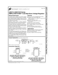
Block and Connection Diagrams<br />
Dual-In-Line Package<br />
<strong>CD4047BM</strong><strong>CD4047BC</strong> <strong>Low</strong> <strong>Power</strong> <strong>Monostable</strong><strong>Astable</strong> <strong>Multivibrator</strong><br />
TLF5969–1<br />
TLF5969–2<br />
Top View<br />
Order Number CD4047B<br />
C1995 National Semiconductor Corporation<br />
TLF5969<br />
RRD-B30M105Printed in U S A
Absolute Maximum Ratings (Notes 1 and 2)<br />
If MilitaryAerospace specified devices are required<br />
please contact the National Semiconductor Sales<br />
OfficeDistributors for availability and specifications<br />
DC Supply Voltage (V DD )<br />
b05V to a18V DC<br />
Input Voltage (V IN )<br />
b05V to V DD a05V DC<br />
Storage Temperature Range (T S ) b65Ctoa150C<br />
<strong>Power</strong> Dissipation (P D )<br />
Dual-In-Line<br />
700 mW<br />
Small Outline<br />
500 mW<br />
Lead Temperature (T L )<br />
(Soldering 10 seconds)<br />
260C<br />
Recommended Operating<br />
Conditions (Note 2)<br />
DC Supply Voltage (V DD )<br />
Input Voltage (V IN )<br />
Operating Temperature Range (T A )<br />
<strong>CD4047BM</strong><br />
<strong>CD4047BC</strong><br />
3Vto15V DC<br />
0 to V DD V DC<br />
b55Ctoa125C<br />
b40Ctoa85C<br />
DC Electrical Characteristics <strong>CD4047BM</strong> (Note 2)<br />
Symbol Parameter Conditions<br />
b55C 25C 125C<br />
Min Max Min Typ Max Min Max<br />
I DD Quiescent Device Current V DD e 5V 5 5 150 mA<br />
V DD e 10V 10 10 300 mA<br />
V DD e 15V 20 20 600 mA<br />
V OL <strong>Low</strong> Level Output Voltage lI Ol k 1 mA<br />
V DD e 5V 005 0 005 005 V<br />
V DD e 10V 005 0 005 005 V<br />
V DD e 15V 005 0 005 005 V<br />
V OH High Level Output Voltage lI Ol k 1 mA<br />
V DD e 5V 495 495 5 495 V<br />
V DD e 10V 995 995 10 995 V<br />
V DD e 15V 1495 1495 15 1495 V<br />
V IL <strong>Low</strong> Level Input Voltage V DD e 5V V O e 05V or 45V 15 225 15 15 V<br />
V DD e 10V V O e 1V or 9V 30 45 30 30 V<br />
V DD e 15V V O e 15V or 135V 40 675 40 40 V<br />
V IH High Level Input Voltage V DD e 5V V O e 05V or 45V 35 35 275 35 V<br />
V DD e 10V V O e 1V or 9V 70 70 55 70 V<br />
V DD e 15V V O e 15V or 135V 110 110 825 110 V<br />
I OL <strong>Low</strong> Level Output Current V DD e 5V V O e 04V 064 051 088 036 mA<br />
(Note 3) V DD e 10V V O e 05V 16 13 225 09 mA<br />
V DD e 15V V O e 15V 42 34 88 24 mA<br />
I OH High Level Output Current V DD e 5V V O e 46V b064 b051 b088 b036 mA<br />
(Note 3) V DD e 10V V O e 95V b16 b13 b225 b09 mA<br />
V DD e 15V V O e 135V b42 b34 b88 b24 mA<br />
I IN Input Current V DD e 15V V IN e 0V b01 b10b5 b01 b10 mA<br />
V DD e 15V V IN e 15V 01 10 b5 01 10 mA<br />
DC Electrical Characteristics <strong>CD4047BC</strong> (Note 2)<br />
Symbol Parameter Conditions<br />
b40C 25C 85C<br />
Min Max Min Typ Max Min Max<br />
I DD Quiescent Device Current V DD e 5V 20 20 150 mA<br />
V DD e 10V 40 40 300 mA<br />
V DD e 15V 80 80 600 mA<br />
V OL <strong>Low</strong> Level Output Voltage lI Ol k 1 mA<br />
V DD e 5V 005 0 005 005 V<br />
V DD e 10V 005 0 005 005 V<br />
V DD e 15V 005 0 005 005 V<br />
V OH High Level Output Voltage lI Ol k 1 mA<br />
V DD e 5V 495 495 5 495 V<br />
V DD e 10V 995 995 10 995 V<br />
V DD e 15V 1495 1495 15 1495 V<br />
Units<br />
Units<br />
2
DC Electrical Characteristics <strong>CD4047BC</strong> (Note 2) (Continued)<br />
Symbol Parameter Conditions<br />
b40C 25C 85C<br />
Min Max Min Typ Max Min Max<br />
V IL <strong>Low</strong> Level Input Voltage V DD e 5V V O e 05V or 45V 15 225 15 15 V<br />
V DD e 10V V O e 1V or 9V 30 45 30 30 V<br />
V DD e 15V V O e 15V or 135V 40 675 40 40 V<br />
V IH High Level Input Voltage V DD e 5V V O e 05V or 45V 35 35 275 35 V<br />
V DD e 10V V O e 1V or 9V 70 70 55 70 V<br />
V DD e 15V V O e 15V or 135V 110 110 825 110 V<br />
I OL <strong>Low</strong> Level Output Current V DD e 5V V O e 04V 052 044 088 036 mA<br />
(Note 3) V DD e 10V V O e 05V 13 11 225 09 mA<br />
V DD e 15V V O e 15V 36 30 88 24 mA<br />
I OH High Level Output Current V DD e 5V V O e 46V b052 b044 b088 b036 mA<br />
(Note 3) V DD e 10V V O e 95V b13 b11 b225 b09 mA<br />
V DD e 15V V O e 135V b36 b30 b88 b24 mA<br />
I IN Input Current V DD e 15V V IN e 0V b03 b10b5 b03 b10 mA<br />
V DD e 15V V IN e 15V 03 10 b5 03 10 mA<br />
Note 1 ‘‘Absolute Maximum Ratings’’ are those values beyond which the safety of the device cannot be guaranteed They are not meant to imply that the devices<br />
should be operated at these limits The table of ‘‘Recommended Operating Conditions’’ and ‘‘Electrical Characteristics’’ provides conditions for actual device<br />
oepration<br />
Note 2 V SS e 0V unless otherwise specified<br />
Note 3 I OH and I OL are tested one output at a time<br />
AC Electrical Characteristics CD4047B<br />
T A e 25C C L e 50 pF R L e 200k input t r e t f e 20 ns unless otherwise specified<br />
Symbol Parameter Conditions Min Typ Max Units<br />
t PHL t PLH Propagation Delay Time <strong>Astable</strong> V DD e 5V 200 400 ns<br />
<strong>Astable</strong> to Osc Out V DD e 10V 100 200 ns<br />
V DD e 15V 80 160 ns<br />
t PHL t PLH <strong>Astable</strong> <strong>Astable</strong> to Q Q V DD e 5V 550 900 ns<br />
V DD e 10V 250 500 ns<br />
V DD e 15V 200 400 ns<br />
t PHL t PLH a Trigger b Trigger to Q V DD e 5V 700 1200 ns<br />
V DD e 10V 300 600 ns<br />
V DD e 15V 240 480 ns<br />
t PHL t PLH a Trigger Retrigger to Q V DD e 5V 300 600 ns<br />
V DD e 10V 175 300 ns<br />
V DD e 15V 150 250 ns<br />
t PHL t PLH Reset to Q Q V DD e 5V 300 600 ns<br />
V DD e 10V 125 250 ns<br />
V DD e 15V 100 200 ns<br />
t THL t TLH Transition Time Q Q Osc Out V DD e 5V 100 200 ns<br />
V DD e 10V 50 100 ns<br />
V DD e 15V 40 80 ns<br />
t WL t WH Minimum Input Pulse Duration Any Input<br />
V DD e 5V 500 1000 ns<br />
V DD e 10V 200 400 ns<br />
V DD e 15V 160 320 ns<br />
t RCL t FCL a Trigger Retrigger Rise and V DD e 5V 15 ms<br />
Fall Time V DD e 10V 5 ms<br />
V DD e 15V 5 ms<br />
C IN Average Input Capacitance Any Input 5 75 pF<br />
AC Parameters are guaranteed by DC correlated testing<br />
Units<br />
3
Logic Diagram<br />
Special input protection circuit to permit larger input-voltage swings<br />
Truth Table<br />
Function<br />
Terminal Connections<br />
Output Pulse<br />
Input Pulse From<br />
To V DD To V SS<br />
To<br />
TLF5969–3<br />
Typical Output<br />
Period or<br />
Pulse Width<br />
<strong>Astable</strong> <strong>Multivibrator</strong><br />
Free-Running 4 5 6 14 7 8 9 12 10 11 13 t A (10 11) e 440 RC<br />
True Gating 4 6 14 7 8 9 12 5 10 11 13<br />
Complement Gating 6 14 5 7 8 9 12 4 10 11 13<br />
t A (13) e 220 RC<br />
<strong>Monostable</strong> <strong>Multivibrator</strong><br />
Positive-Edge Trigger 4 14 5 6 7 9 12 8 10 11<br />
Negative-Edge Trigger 4 8 14 5 7 9 12 6 10 11 t M (10 11) e 248 RC<br />
Retriggerable 4 14 5 6 7 9 8 12 10 11<br />
External Countdown<br />
14 5 6 7 8 9 12 (See Figure) (See Figure) (See Figure)<br />
Note External resistor between terminals 2 and 3 External capacitor between terminals 1 and 3<br />
Typical Implementation of External Countdown Option<br />
t EXT e (N b 1) t A a (t M a t A 2)<br />
TLF5969–4<br />
4
Typical Performance Characteristics<br />
Typical Q Q Osc Out Period<br />
Accuracy vs Supply Voltage<br />
(<strong>Astable</strong> Mode Operation)<br />
Typical Q Q Pulse Width<br />
Accuracy vs Supply Voltage<br />
<strong>Monostable</strong> Mode Operation<br />
TLF5969–5<br />
f Q Q R C<br />
A 1000 kHz 22k 10 pF<br />
B 100 kHz 22k 100 pF<br />
C 10 kHz 220k 100 pF<br />
D 1 kHz 220k 1000 pF<br />
E 100 Hz 22M 1000 pF<br />
TLF5969–6<br />
t M R C<br />
A 2 ms 22k 10 pF<br />
B 7 ms 22k 100 pF<br />
C 60 ms 220k 100 pF<br />
D 550 ms 220k 1000 pF<br />
E 55 ms 22M 1000 pF<br />
Typical Q Q and Osc Out<br />
Period Accuracy vs Temperature<br />
<strong>Astable</strong> Mode Operation<br />
Typical Q and Q Pulse Width<br />
Accuracy vs Temperature<br />
<strong>Monostable</strong> Mode Operation<br />
TLF5969–7<br />
f Q Q R C<br />
A 1000 kHz 22k 10 pF<br />
B 100 kHz 22k 100 pF<br />
C 10 kHz 220k 100 pF<br />
D 1 kHz 220k 1000 pF<br />
Timing Diagram<br />
<strong>Astable</strong> Mode<br />
TLF5969–8<br />
t M R C<br />
A 2 ms 22k 10 pF<br />
B 7 ms 22k 100 pF<br />
C 60 ms 220k 100 pF<br />
D 550 ms 220k 1000 pF<br />
<strong>Monostable</strong> Mode<br />
TLF5969–9<br />
TLF5969–10<br />
Retrigger Mode<br />
TLF5969–11<br />
5
<strong>CD4047BM</strong><strong>CD4047BC</strong> <strong>Low</strong> <strong>Power</strong> <strong>Monostable</strong><strong>Astable</strong> <strong>Multivibrator</strong><br />
Physical Dimensions inches (millimeters)<br />
LIFE SUPPORT POLICY<br />
Order Number <strong>CD4047BM</strong>J or <strong>CD4047BC</strong>J<br />
NS Package Number J14A<br />
Order Number <strong>CD4047BM</strong>N or <strong>CD4047BC</strong>N<br />
NS Package Number N14A<br />
NATIONAL’S PRODUCTS ARE NOT AUTHORIZED FOR USE AS CRITICAL COMPONENTS IN LIFE SUPPORT<br />
DEVICES OR SYSTEMS WITHOUT THE EXPRESS WRITTEN APPROVAL OF THE PRESIDENT OF NATIONAL<br />
SEMICONDUCTOR CORPORATION As used herein<br />
1 Life support devices or systems are devices or 2 A critical component is any component of a life<br />
systems which (a) are intended for surgical implant support device or system whose failure to perform can<br />
into the body or (b) support or sustain life and whose be reasonably expected to cause the failure of the life<br />
failure to perform when properly used in accordance support device or system or to affect its safety or<br />
with instructions for use provided in the labeling can effectiveness<br />
be reasonably expected to result in a significant injury<br />
to the user<br />
National Semiconductor National Semiconductor National Semiconductor National Semiconductor<br />
Corporation Europe Hong Kong Ltd Japan Ltd<br />
1111 West Bardin Road Fax (a49) 0-180-530 85 86 13th Floor Straight Block Tel 81-043-299-2309<br />
Arlington TX 76017 Email cnjwge tevm2nsccom Ocean Centre 5 Canton Rd Fax 81-043-299-2408<br />
Tel 1(800) 272-9959 Deutsch Tel (a49) 0-180-530 85 85 Tsimshatsui Kowloon<br />
Fax 1(800) 737-7018 English Tel (a49) 0-180-532 78 32 Hong Kong<br />
Franais Tel (a49) 0-180-532 93 58 Tel (852) 2737-1600<br />
Italiano Tel (a49) 0-180-534 16 80 Fax (852) 2736-9960<br />
National does not assume any responsibility for use of any circuitry described no circuit patent licenses are implied and National reserves the right at any time without notice to change said circuitry and specifications