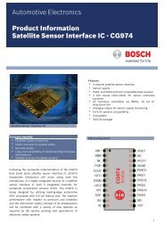
Download Link - Bosch Semiconductors and Sensors
Download Link - Bosch Semiconductors and Sensors
Download Link - Bosch Semiconductors and Sensors

Create successful ePaper yourself
Turn your PDF publications into a flip-book with our unique Google optimized e-Paper software.
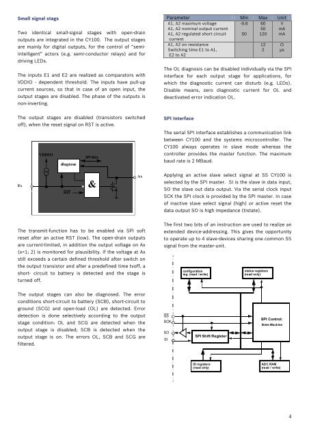
Small signal stags<br />
Two identical small-signal stages with open-drain<br />
outputs are integrated in the CY100. The output stages<br />
are mainly for digital outputs, for the control of “semiintelligent”<br />
actors (e.g. semi-conductor relays) <strong>and</strong> for<br />
driving LEDs.<br />
The inputs E1 <strong>and</strong> E2 are realized as comparators with<br />
VDDIO - dependent threshold. The inputs have pull-up<br />
current sources, so that in case of an open input, the<br />
output stages are disabled. The phase of the outputs is<br />
non-inverting.<br />
Parameter Min Max Unit<br />
A1, A2 maximum voltage<br />
A1, A2 nominal output current<br />
A1, A2 regulated short circuit<br />
current<br />
-0.6<br />
50<br />
60<br />
50<br />
120<br />
V<br />
mA<br />
mA<br />
A1, A2 on resistance<br />
Switching time E1 to A1,<br />
E2 to A2<br />
12<br />
2<br />
Ω<br />
µs<br />
The OL diagnosis can be disabled individually via the SPI<br />
interface for each output stage for applications, for<br />
which the diagnostic current can disturb (e.g. LEDs).<br />
Disable means, zero diagnostic current for OL <strong>and</strong><br />
deactivated error indication OL.<br />
The output stages are disabled (transistors switched<br />
off), when the reset signal on RST is active.<br />
VDDIO<br />
SPI-Bits<br />
diagnose<br />
SPI Interface<br />
The serial SPI interface establishes a communication link<br />
between CY100 <strong>and</strong> the systems microcontroller. The<br />
CY100 always operates in slave mode whereas the<br />
controller provides the master function. The maximum<br />
baud rate is 2 MBaud.<br />
Ex<br />
RST<br />
&<br />
Ax<br />
Applying an active slave select signal at SS CY100 is<br />
selected by the SPI master. SI is the slave in data input,<br />
SO the slave out data output. Via the serial clock input<br />
SCK the SPI clock is provided by the SPI master. In case<br />
of inactive slave select signal (high) or active reset the<br />
data output SO is high impedance (tistate).<br />
The transmit-function has to be enabled via SPI soft<br />
reset after an active RST (low). The open-drain outputs<br />
are current-limited, in addition the output voltage on Ax<br />
(x=1; 2) is monitored for plausibility. If the voltage at Ax<br />
still exceeds a certain defined threshold after switch on<br />
the output transistor <strong>and</strong> after a predefined time tvoff, a<br />
short- circuit to battery is detected <strong>and</strong> the stage is<br />
turned off.<br />
The first two bits of an instruction are used to realize an<br />
extended device-addressing. This gives the opportunity<br />
to operate up to 4 slave-devices sharing one common SS<br />
signal from the master-unit.<br />
configuration<br />
reg. (read / write)<br />
status registers<br />
(read only)<br />
The output stages can also be diagnosed. The error<br />
conditions short-circuit to battery (SCB), short-circuit to<br />
ground (SCG) <strong>and</strong> open-load (OL) are detected. Error<br />
detection is done selectively according to the output<br />
stage condition: OL <strong>and</strong> SCG are detected when the<br />
output stage is disabled; SCB is detected when the<br />
output stage is on. The errors OL, SCB <strong>and</strong> SCG are<br />
filtered.<br />
SS<br />
SCK<br />
SO<br />
SI<br />
SPI Shift Register<br />
SPI Control:<br />
State Machine<br />
ID registers<br />
(read only)<br />
ADC RAM<br />
(read / write)<br />
4