Substrate Bumping for Micro BGA - Speedline Technologies
Substrate Bumping for Micro BGA - Speedline Technologies
Substrate Bumping for Micro BGA - Speedline Technologies

Create successful ePaper yourself
Turn your PDF publications into a flip-book with our unique Google optimized e-Paper software.
<strong>Substrate</strong> Printing <strong>for</strong> <strong>Micro</strong> <strong>BGA</strong><br />
Rita Mohanty<br />
<strong>Speedline</strong> <strong>Technologies</strong><br />
16 Forge Parkway<br />
Franklin, MA<br />
508-541-4762<br />
rmohanty@speedlinetech.com<br />
Abstract<br />
As the demand <strong>for</strong> faster, smaller, cheaper and smarter electronic products such as cell phones, pagers and PDAs<br />
increases, the demand on packaging footprint also increases. Flip chip and micro <strong>BGA</strong> are the ideal responses to<br />
the demand <strong>for</strong> more functionality and compact packaging. But the assembly of flip chip and micro <strong>BGA</strong> comes with<br />
its own challenges. The primary challenge is to provide reliable mechanical and electrical interconnection. The<br />
most cost effective way to provide both mechanical and electrical interconnection is the application of solder paste<br />
via stencil printing process.<br />
Stencil printing is a common process in surface mount and other packaging process. The guidelines <strong>for</strong> stencil<br />
design, paste <strong>for</strong>mulation and printing equipment are well developed <strong>for</strong> mainstream SMT process. When it comes<br />
to ultra fine pitch application, some of the previously developed guidelines may no longer hold. New guidelines may<br />
need to be developed to address the requirements of ultra fine pitch printing. Most assemblers believe that 50-70%<br />
of the end of the line defects contribute to the stencil printing process. Controlling the amount of solder paste<br />
deposit to meet the ultra fine pitch application is critical to the process.<br />
This paper will describe work done in the area of micro <strong>BGA</strong> assembly using various stencil designs, materials and<br />
process factors through a series of design of experiment. Bump size of 65 microns to 150 microns will be the focus<br />
of this discussion.<br />
Key words: <strong>Substrate</strong> bumping, solder paste printing, SPI inspection, Print DOE, Transfer efficiency<br />
Introduction:<br />
The flip chip technology has been one of the<br />
key enablers in the advancement of smaller, cheaper<br />
and faster packaging design. It provides excellent<br />
electrical per<strong>for</strong>mance and high I/O’s handling<br />
capability compared to traditional wire bonding<br />
technology. Flip chip technology was originally<br />
developed <strong>for</strong> computer and notebook PC to improve<br />
miniaturization and per<strong>for</strong>mance. Here, per<strong>for</strong>mance<br />
took priority over cost. As we start to apply this<br />
technology to consumer products, cost becomes as<br />
important as the per<strong>for</strong>mance. There are two distinct<br />
ways to address the second level electrical connection<br />
need - bumping the wafer or bumping the substrate.<br />
Traditionally, wafer bumping has been the<br />
mainstream approach. As the pressure <strong>for</strong> cost<br />
reduction has increased <strong>for</strong> the semiconductor<br />
packaging industry, people have investigated<br />
bumping lower cost organic substrate as an<br />
alternative.<br />
There are several solder bumping<br />
technologies <strong>for</strong> substrate bumping. These are<br />
evaporation, electroplating, solder paste deposition<br />
and others. Evaporation is well-documented and<br />
highly reliable, with extremely fine pitch capability.<br />
Yet, it is considerably expensive, relatively slow and<br />
capital-intensive. The more common processes<br />
implemented today are electroplating and solder<br />
paste deposition. Electroplating is a complex process<br />
that involves several steps that can be considered<br />
environmentally unfriendly. The solder paste<br />
deposition is a simpler, faster, cheaper and<br />
environmentally friendly process. In this process, a<br />
metal mask with an opening <strong>for</strong> the pad area is used<br />
to deposit solder paste. Solder paste is printed onto<br />
the substrate and reflowed once. Because of overall<br />
faster throughput, solder paste printing is lower in<br />
cost compared to electroplating. While electroplating<br />
offers finer pitch capability, solder paste printing<br />
offers material flexibility, which presents advantages<br />
when considering Pb-free packages. Because of the
varying plating rates required <strong>for</strong> the Pb-free solders<br />
that are typically ternary alloys, electroplating has<br />
difficulty controlling compositions. In general,<br />
ternary alloys are a greater challenge because they<br />
require more complex equipment and photo-resist<br />
processing. Solder paste printing, on the other hand,<br />
offers greater composition control and material<br />
flexibility to support Pb-free alloys.<br />
Background:<br />
Though there are several advantages to the<br />
solder paste printing process, there are also<br />
challenges and limitations associated with printing.<br />
Namely, these are printing solder paste deposits that<br />
are large enough to produce bumps with the required<br />
height and co-planarity within the constraints of the<br />
pitches. The difficulty lies with the stencil<br />
manufacturing technologies and solder paste<br />
limitations. When printing full area array designs, the<br />
slumping of the overprinted solder paste results in<br />
solder robbing during reflow process. There<strong>for</strong>e, it is<br />
very important to use a paste and stencil technology<br />
which promotes easy release of the paste and has<br />
adequate slump resistance during print and reflow. In<br />
this study, per<strong>for</strong>mance of two different paste<br />
chemistries is evaluated.<br />
The following factors are critical to achieve<br />
successful bumping using solder paste printing:<br />
• Printing technique<br />
• Stencil design<br />
• Paste <strong>for</strong>mulation<br />
• Reflow process<br />
• <strong>Substrate</strong> flatness<br />
The current study focuses on the printing part of the<br />
bumping process. Printing is a highly complex<br />
process and is considered to be “black magic” by<br />
many experts. The goal here is to demystify the<br />
printing process through a series of well designed<br />
experiment. Results from the evaluation of the<br />
printing technique and paste chemistries are<br />
presented in this paper.<br />
Test Vehicle:<br />
The test vehicle used <strong>for</strong> the study was a two<br />
layer FR4 substrate. The thickness of the substrate<br />
was 0.012” with 0.5oz copper and Immersion Nickel<br />
Gold (ING) pad finish. The substrate was designed to<br />
include extreme cases, (extremely small pad size and<br />
web size) to understand the limitation of the stencil<br />
printing capability. The pad size varied from 200µ to<br />
65µ, as shown in figure 1. In addition to various pad<br />
sizes, the pitch/web was also varied to understand the<br />
effects of the above factors on the printing capability.<br />
The details of the pad size, pitch and web dimension<br />
are shown in table 1. Figure 2 shows an expanded<br />
view of an 200µ (8mil) pad design. For better data<br />
management, each group of pads was assigned a<br />
location number., the top left group being LN1 and<br />
the bottom right being LN36.<br />
Each location contained an array of 25X25 pads.<br />
Some arrays were repeated on the board to<br />
understand the printing characteristic as a function of<br />
location. To keep the scope of the initial experiment<br />
manageable, only the areas shaded in white (10X10)<br />
were inspected <strong>for</strong> transfer efficiency data.<br />
Web<br />
150µ LN1<br />
125µ<br />
100µ LN3<br />
LN36<br />
Pad size 200µ 175µ 150µ 125µ 100µ 65µ<br />
Figure 1. Test Vehicle showing pad locations used in the SPI inspection scheam.
Table 1. Pad design<br />
Pad size,<br />
<strong>Micro</strong>ns<br />
Web,<br />
<strong>Micro</strong>ns<br />
Pitch,<br />
<strong>Micro</strong>ns<br />
Area<br />
Ratio<br />
200 (LN1-3) 150, 125, 100 350, 325, 300 0.70<br />
175 (LN4-6) 150, 125, 100 325, 300, 275 0.80<br />
Figure 3. Stencil design<br />
150 (LN7-9) 150, 125, 100 300, 275, 250 0.93<br />
125 (LN10-12) 150, 125, 100 275, 250, 225 1.12<br />
100 150, 125, 100 250, 225, 200 1.40<br />
75 100, 75, 50 175, 150, 125 1.87<br />
50 100, 75, 50 150, 125, 100 2.80<br />
Pitch-350µ<br />
200µ 150µ 200µ<br />
200µ 125µ 200µ<br />
200µ<br />
100µ<br />
Pitch-300µ<br />
200µ<br />
Figure 2. An example of the pad layout showing<br />
200µ pad size and corresponding pitch/web.<br />
Stencil Design:<br />
It is well known that the stencil design is a<br />
critical factor affecting the transfer efficiency of any<br />
printing process. Print volume and consistency <strong>for</strong><br />
small deposit could be maximized by carefully<br />
choosing the stencil design parameters. Keeping this<br />
in mind, the stencil <strong>for</strong> this study was chosen to be a<br />
35 micron thick electro<strong>for</strong>m stencil. The aperture size<br />
and pitch was in 1:1 ratio with the land pattern. The<br />
stencil apertures were designed as squares to<br />
maximize the amount of paste deposited per site.<br />
Figure 3 and 4 shows the layout of the stencil.<br />
Figure 4. Expanded view of the stencil layout.<br />
Paste type:<br />
The pastes used in this study consisted of<br />
type 6 powder with both water base and no clean<br />
chemistry.<br />
Experimental:<br />
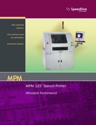
A MPM Accela printer with Rheopump was<br />
used in this study. Due to the thin nature of the<br />
substrate, a dedicated tool with an external venture<br />
pump was used to hold the substrate flat <strong>for</strong> the<br />
printing experiment. During the experiment, the<br />
Rheopum chamber pressure was held constant at 1.0<br />
psi. Several boards were printed to stabilize the<br />
chamber pressure be<strong>for</strong>e the actual DOE was run. To<br />
eliminate paste simmering, the stencil was cleaned<br />
with solvent and vacuum after each print.<br />
Print DOE<br />
The factors and level setting <strong>for</strong> the print<br />
DOE is shown in table 2. As it can be seen from this<br />
table, the experiment consisted of three factors, two<br />
levels, and full factorial design. The response <strong>for</strong> the<br />
print experiment was wet paste volume and height. A<br />
Kho Young (KY300) Solder Paste Inspection (SPI)<br />
system was used to characterize the print quality,<br />
paste volume and paste height. In addition, optical<br />
images of the printed board were also collected to<br />
obtain qualitative data.
Table 2: Factors and level <strong>for</strong> print DOE<br />
Results and Discussion:<br />
The standard order design table <strong>for</strong> the printing<br />
experiment is shown in figure 2. A “repeat” noise<br />
strategy was adopted <strong>for</strong> this experiment to address<br />
run-to-run variations. The board was designed to<br />
understand the effect of various pad size, web size<br />
and pad location. Figure 5 shows the sampling<br />
strategy <strong>for</strong> the study presented here. To make the<br />
discussion simple, results from two locations are<br />
presented here. Figures 6 & 7 shows the main effect<br />
plot and pareto chart <strong>for</strong> no-clean paste <strong>for</strong> location 4<br />
(pad size 200µ) and location 12 (pad size 125µ)<br />
respectively.<br />
To minimize noise, the experiment was fully<br />
randomized with 4 repeats (4 boards per run order).<br />
The noise was further controlled by printing all 4<br />
boards with one print stroke only; front to rear<br />
squeegee direction.<br />
There were several challenges encountered during the<br />
experimental stage: the biggest one being the<br />
limitation of KY 300 to inspect deposit size below<br />
100 microns. There<strong>for</strong>e, data from pads under 100<br />
microns were excluded from the analysis process.<br />
Gage R&R<br />
To ensure minimum experimental variability a Gage<br />
R&R study was conducted on the KY300 SPI by<br />
inspecting one printed board 20 times. Results from<br />
the gage study are shown in table 3. Both volume and<br />
height repeatability are well within the acceptable<br />
range. Based on this result, the gage was considered<br />
to be adequate.<br />
Table 3. Gage R&R from KY300<br />
Volume Repeatability = 15.198 % (3 Sigma)<br />
Height Repeatability = 4.843 um (3 Sigma)<br />
Pad #of<br />
Pad<br />
Size<br />
X<br />
Size<br />
Y<br />
Solder<br />
shape<br />
Vol<br />
GRR<br />
Ht<br />
GRR<br />
0 1875 0.198 0.198 1 8.929 1.827<br />
1 525 0.178 0.178 1 6.052 1.278<br />
Figure 5. DOE sampling strategy<br />
Mean TE<br />
50.29683<br />
70<br />
65<br />
60<br />
50<br />
45<br />
40<br />
35<br />
-1<br />
-0.5<br />
0<br />
0.5<br />
0<br />
Print Speed<br />
1<br />
Term<br />
Print Pressure<br />
Print Speed*Separation Speed<br />
Print Speed*Print Pressure<br />
Separation Speed<br />
Print Speed*Print Pressure*Separation Speed<br />
Print Pressure*Separation Speed<br />
Print Speed<br />
-1<br />
-0.5<br />
Estimate<br />
-7.594489<br />
-5.036974<br />
-4.416037<br />
3.258721<br />
2.457414<br />
-2.103566<br />
0.946250<br />
0<br />
0.5<br />
0<br />
Print<br />
Pressure<br />
1<br />
-1<br />
-0.5<br />
0<br />
0.5<br />
0<br />
Separation<br />
Speed<br />
Figure 6. Result <strong>for</strong> no-clean paste, location 4.<br />
Mean TE<br />
37.16677<br />
50<br />
45<br />
40<br />
35<br />
30<br />
25<br />
20<br />
-1<br />
-0.5<br />
0<br />
0.5<br />
0<br />
Print Speed<br />
1<br />
Term<br />
Print Speed*Print Pressure*Separation Speed<br />
Print Speed<br />
Print Speed*Print Pressure<br />
Separation Speed<br />
Print Speed*Separation Speed<br />
Print Pressure*Separation Speed<br />
Print Pressure<br />
Main effect plot<br />
Main effect plot<br />
-1<br />
-0.5<br />
Estimate<br />
5.421119<br />
-3.995863<br />
-2.484561<br />
1.749264<br />
0.634162<br />
-0.612079<br />
0.050882<br />
0<br />
0.5<br />
0<br />
Print<br />
Pressure<br />
1<br />
Pareto chart<br />
-1<br />
-0.5<br />
Pareto chart<br />
0<br />
0.5<br />
0<br />
Separation<br />
Speed<br />
Figure 7. Result <strong>for</strong> no-clean paste, location 12.<br />
1<br />
1
Figure 7 and 8 shows the two locations<br />
behave very differently. Specially as the pad size<br />
decreases, complex interactions becomes very<br />
important <strong>for</strong> the printing process. This is evidenced<br />
by the three way interaction <strong>for</strong> the 125µ pad size.<br />
Result <strong>for</strong> the water base paste <strong>for</strong> location 4<br />
(175µ pad) is shown in figure 8. We see here the<br />
main effect is different from no clean paste and<br />
interaction do play an important role in the TE.<br />
Mean TE<br />
53.06897<br />
100<br />
80<br />
60<br />
40<br />
20<br />
-1<br />
-0.5<br />
0<br />
0.5<br />
0<br />
Print Speed<br />
1<br />
Term<br />
Print Speed*Print Pressure<br />
Print Speed*Separation Speed<br />
Print Speed<br />
Print Pressure<br />
Print Pressure*Separation Speed<br />
Print Speed*Print Pressure*Separation Speed<br />
Separation Speed<br />
-1<br />
-0.5<br />
Estimate<br />
14.25263<br />
-13.56193<br />
-7.63410<br />
-3.87919<br />
-3.75609<br />
-3.11402<br />
0.48576<br />
0<br />
0.5<br />
0<br />
Print<br />
Pressure<br />
1<br />
-1<br />
-0.5<br />
0<br />
0.5<br />
0<br />
Separation<br />
Speed<br />
Figure 8. Result <strong>for</strong> water base paste, location 4.<br />
1<br />
Figure 9. No clean “Paste on pad” images of various pad and web size. 8 and 2 refers to<br />
pad size in mils and W1‐3 refers to web size of 6,5 and 4 mil<br />
Figure 10. Water soluble “Paste on pad” images of various pad and web size. 8<br />
and 2 refers to pad size in mils and W1‐3 refers to web size of 6,5 and 4 mil
Based on the DOE analysis, an optimum factor<br />
combination was determined <strong>for</strong> each type of paste<br />
and the result is presented below.<br />
Optical micrographs <strong>for</strong> both types of pastes are<br />
shown in figures 9 and 10. Pad sizes smaller than 100<br />
microns (4mil) showed acceptable paste transfer<br />
(qualitatively) but the registration was very poor<br />
(paste was printed of the pads) due to board stretch.<br />
In addition, the SPI machine used in this study was<br />
not able to inspect deposit below 100 microns size.<br />
Hence the result and discussion is restricted to pad<br />
size above 100 microns.<br />
As it can be seen from the above figures, the<br />
deposits were well <strong>for</strong>med without any bridging or<br />
insufficient <strong>for</strong> 200µ pad size. As the pad size<br />
decreased, even with higher area ratio, the paste<br />
transfer deteriorated due to extremely small aperture<br />
opening.<br />
Figures 11 shows the effect of pad size and<br />
web on the overall transfer efficiency <strong>for</strong> both noclean<br />
and water base paste.<br />
Figure 11. Effect of pad and web size on paste transfer efficiency<br />
Effect of paste chemistry:<br />
Paste chemistry appears to have a significant<br />
effect on the paste transfer characteristic. No clean<br />
paste provides a more consistent paste transfer as<br />
would be predicted by the aperture size. However,<br />
water soluble paste shows inconsistent paste transfer<br />
<strong>for</strong> 200µ and 175µ pad size. Further investigation is<br />
necessary to fully understand the phenomena<br />
exhibited here.<br />
Effect of pad/aperture size:<br />
As one would expect, larger pad size<br />
provides better transfer efficiency regardless of the<br />
area ratio. As it was mentioned above, the<br />
inconsistency of water base paste <strong>for</strong> the 200µ pad<br />
will require further investigation to confirm the<br />
finding.<br />
Effect of web size:<br />
Web size shows no effect on the paste<br />
transfer efficiency. The critical factor to watch here<br />
would be the stencil life span. As the web size<br />
becomes smaller and smaller, the potential <strong>for</strong> stencil<br />
damage becomes higher.<br />
Summary<br />
As this work was an initial attempt at understanding<br />
the complex printing process associated with fine<br />
pitch printing, the experiment raised more questions<br />
than answers. It is clear that the paste chemistry plays<br />
an important role in the overall printing per<strong>for</strong>mance<br />
when it comes to bumping application. It is also clear<br />
that pad size below 150µ becomes a challenge <strong>for</strong><br />
stencil printing.<br />
Another important observation from this<br />
experiment is that strong interactions exist between<br />
various factors. The factors include both printing<br />
parameters, board design and paste type.
Further investigation is necessary to fully<br />
understand the interaction between various factors<br />
and set guideline <strong>for</strong> substrate bumping process using<br />
stencil printing process.<br />
Acknowledgment:<br />
The author would like to thank Vatsal Shah<br />
from <strong>Speedline</strong> <strong>Technologies</strong> <strong>for</strong> conducting all the<br />
experiments and assisting with data analysis. The<br />
author would also like to thank Ed Briggs from<br />
Indium Corp. <strong>for</strong> providing the paste and process<br />
knowledge which was critical in completing this<br />
study.