SPD9441 Radiation Detector PIN Diode - Solid State Devices, Inc.
SPD9441 Radiation Detector PIN Diode - Solid State Devices, Inc.
SPD9441 Radiation Detector PIN Diode - Solid State Devices, Inc.

You also want an ePaper? Increase the reach of your titles
YUMPU automatically turns print PDFs into web optimized ePapers that Google loves.
<strong>SPD9441</strong> <strong>Radiation</strong> <strong>Detector</strong> <strong>PIN</strong> <strong>Diode</strong><br />
AN2011-01<br />
Introduction<br />
<strong>SPD9441</strong> <strong>Radiation</strong> <strong>Detector</strong> <strong>PIN</strong> <strong>Diode</strong>s are high efficiency detectors of nuclear and electromagnetic radiation including<br />
gamma radiation, electron radiation and x-rays. Utilizing a high reliability construction method, the <strong>SPD9441</strong><br />
has an operating and storage temperature range of -65°C to +200°C and will survive liquid to liquid cryogenic thermal<br />
cycling of -180°C to +100°C. This device is a direct replacement for the UM9441 and is characterized by a high photocurrent<br />
sensitivity and ceramic frit glass construction noted for high reliability.<br />
Description<br />
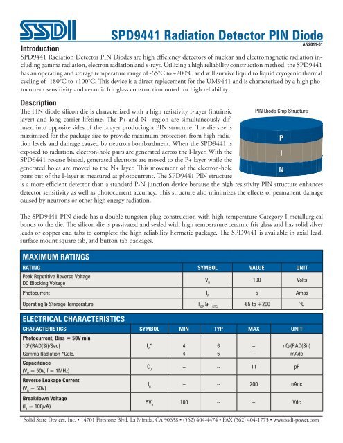
The <strong>PIN</strong> diode silicon die is characterized with a high resistivity I-layer (intrinsic <strong>PIN</strong> <strong>Diode</strong> Chip Structure<br />
layer) and long carrier lifetime. The P+ and N+ region are simultaneously diffused<br />
into opposite sides of the I-layer producing a <strong>PIN</strong> structure. The die size is<br />
maximized for the package size to provide maximum protection from high radiation<br />
levels and damage caused by neutron bombardment. When the <strong>SPD9441</strong> is<br />
P<br />
exposed to radiation, electron-hole pairs are generated across the I-layer. With the<br />
I<br />
<strong>SPD9441</strong> reverse biased, generated electrons are moved to the P+ layer while the<br />
generated holes are moved to the N+ layer. This movement of the electron-hole<br />
N<br />
pairs out of the I-layer is measured as photocurrent. The <strong>SPD9441</strong> <strong>PIN</strong> structure<br />
is a more efficient detector than a standard P-N junction device because the high resistivity <strong>PIN</strong> structure enhances<br />
detector sensitivity as well as photocurrent accuracy. This structure also minimizes the effects of permanent damage<br />
caused by neutrons or other high energy radiation.<br />
The <strong>SPD9441</strong> <strong>PIN</strong> diode has a double tungsten plug construction with high temperature Category I metallurgical<br />
bonds to the die. The silicon die is passivated and sealed with high temperature ceramic frit glass and has solid silver<br />
leads or copper end tabs to complete the high reliability hermetic package. The <strong>SPD9441</strong> is available in axial lead,<br />
surface mount square tab, and button tab packages.<br />
MAXIMUM RATINGS<br />
RATING SYMBOL VALUE UNIT<br />
Peak Repetitive Reverse Voltage<br />
DC Blocking Voltage<br />
ELECTRICAL CHARACTERISTICS<br />
CHARACTERISTICS SYMBOL MIN TYP MAX UNIT<br />
Photocurrent, Bias = 50V min<br />
10 6 (RAD(Si)/Sec)<br />
Gamma <strong>Radiation</strong> *Calc.<br />
Capacitance<br />
(V R<br />
= 50V, f = 1MHz)<br />
Reverse Leakage Current<br />
(V R<br />
= 50V)<br />
Breakdown Voltage<br />
(I R<br />
= 100µA)<br />
I P<br />
* 4<br />
4<br />
V R<br />
100 Volts<br />
Photocurrent I P<br />
5 Amps<br />
Operating & Storage Temperature T OP<br />
& T STG<br />
-65 to +200 °C<br />
<strong>Solid</strong> <strong>State</strong> <strong>Devices</strong>, <strong>Inc</strong>. ▪ 14701 Firestone Blvd. La Mirada, CA 90638 ▪ (562) 404-4474 ▪ FAX (562) 404-1773 ▪ www.ssdi-power.com<br />
6<br />
6<br />
--<br />
--<br />
nQ/(RAD(Si))<br />
mAdc<br />
C J<br />
-- -- 11 pF<br />
I R<br />
-- -- 200 nAdc<br />
BV R<br />
100 -- -- Vdc
<strong>SPD9441</strong> <strong>Radiation</strong> <strong>Detector</strong> <strong>PIN</strong> <strong>Diode</strong><br />
AN2011-01<br />
Axial<br />
DIM MIN MAX<br />
A -- .200”<br />
B -- .300”<br />
C .037” .041”<br />
D .75” --<br />
D B D<br />
ØC ØA<br />
Surface Mount Square Tab (SMS)<br />
DIM MIN MAX<br />
A .195” .200”<br />
B -- .350”<br />
C .019” .027”<br />
D .002” --<br />
D<br />
C<br />
B<br />
A<br />
A<br />
Button Tab<br />
DIM MIN MAX<br />
A -- .310”<br />
A1 -- .020”<br />
ØB -- .190”<br />
C .190” .210”<br />
C1<br />
.280” REF<br />
P1 .145” .155”<br />
P2 .055” .075”<br />
P3 .090” .110”<br />
P4<br />
.060” REF<br />
T .008” .012”<br />
R<br />
.015” REF<br />
CATHODE<br />
ØP1<br />
P4<br />
P2<br />
ANODE<br />
T<br />
A<br />
A1<br />
2x R<br />
C<br />
OPTIONAL TAB PROFILE<br />
ØB<br />
C1<br />
P3<br />
<strong>Solid</strong> <strong>State</strong> <strong>Devices</strong>, <strong>Inc</strong>. ▪ 14701 Firestone Blvd. La Mirada, CA 90638 ▪ (562) 404-4474 ▪ FAX (562) 404-1773 ▪ www.ssdi-power.com