256K (32K x 8) 5-volt Only Flash Memory AT29C256
256K (32K x 8) 5-volt Only Flash Memory AT29C256
256K (32K x 8) 5-volt Only Flash Memory AT29C256

Create successful ePaper yourself
Turn your PDF publications into a flip-book with our unique Google optimized e-Paper software.
Features<br />
• Fast Read Access Time – 70 ns<br />
• 5-<strong>volt</strong> <strong>Only</strong> Reprogramming<br />
• Page Program Operation<br />
– Single Cycle Reprogram (Erase and Program)<br />
– Internal Address and Data Latches for 64 Bytes<br />
• Internal Program Control and Timer<br />
• Hardware and Software Data Protection<br />
• Fast Program Cycle Times<br />
– Page(64Byte)ProgramTime–10ms<br />
– Chip Erase Time– 10 ms<br />
• DATA Polling for End of Program Detection<br />
• Low-power Dissipation<br />
– 50mAActiveCurrent<br />
–300 µA CMOS Standby Current<br />
• Typical Endurance > 10,000 Cycles<br />
• Single 5V ± 10% Supply<br />
• CMOS and TTL Compatible Inputs and Outputs<br />
• Commercial and Industrial Temperature Ranges<br />
<strong>256K</strong> (<strong>32K</strong> x 8)<br />
5-<strong>volt</strong> <strong>Only</strong><br />
<strong>Flash</strong> <strong>Memory</strong><br />
<strong>AT29C256</strong><br />
Description<br />
The <strong>AT29C256</strong> is a five-<strong>volt</strong>-only in-system <strong>Flash</strong> programmable and erasable read<br />
only memory (PEROM). Its <strong>256K</strong> of memory is organized as 32,768 words by 8 bits.<br />
Manufactured with Atmel’s advanced nonvolatile CMOS technology, the device offers<br />
access times to 70 ns with power dissipation of just 275 mW. When the device is<br />
deselected, the CMOS standby current is less than 300 µA. The device endurance is<br />
such that any sector can typically be written to in excess of 10,000 times.<br />
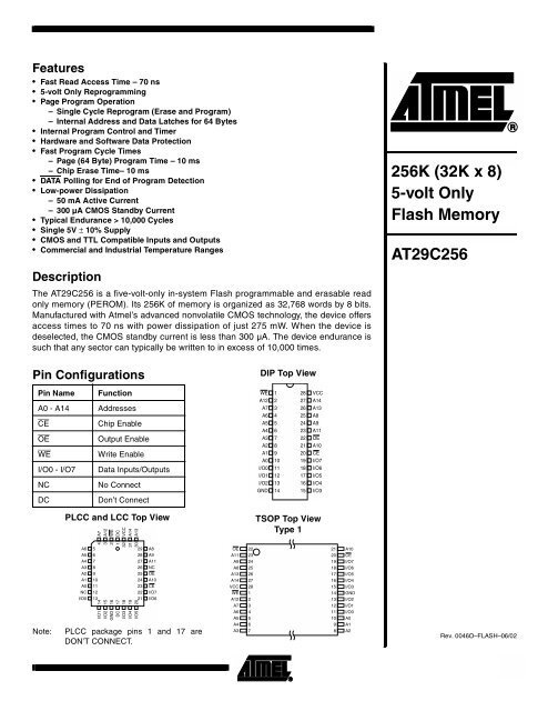
Pin Configurations<br />
DIP Top View<br />
Pin Name<br />
A0 - A14<br />
CE<br />
OE<br />
WE<br />
I/O0 - I/O7<br />
NC<br />
DC<br />
Function<br />
Addresses<br />
Chip Enable<br />
Output Enable<br />
Write Enable<br />
Data Inputs/Outputs<br />
No Connect<br />
Don’t Connect<br />
WE<br />
A12<br />
A7<br />
A6<br />
A5<br />
A4<br />
A3<br />
A2<br />
A1<br />
A0<br />
I/O0<br />
I/O1<br />
I/O2<br />
GND<br />
1<br />
2<br />
3<br />
4<br />
5<br />
6<br />
7<br />
8<br />
9<br />
10<br />
11<br />
12<br />
13<br />
14<br />
28<br />
27<br />
26<br />
25<br />
24<br />
23<br />
22<br />
21<br />
20<br />
19<br />
18<br />
17<br />
16<br />
15<br />
VCC<br />
A14<br />
A13<br />
A8<br />
A9<br />
A11<br />
OE<br />
A10<br />
CE<br />
I/O7<br />
I/O6<br />
I/O5<br />
I/O4<br />
I/O3<br />
PLCC and LCC Top View<br />
A7<br />
A12<br />
WE<br />
DC<br />
VCC<br />
A14<br />
A13<br />
TSOP Top View<br />
Type 1<br />
Note:<br />
A6<br />
A5<br />
A4<br />
A3<br />
A2<br />
A1<br />
A0<br />
NC<br />
I/O0<br />
5<br />
6<br />
7<br />
8<br />
9<br />
10<br />
11<br />
12<br />
13<br />
4<br />
3<br />
2<br />
1<br />
32<br />
31<br />
30<br />
14<br />
15<br />
16<br />
17<br />
18<br />
19<br />
20<br />
I/O1<br />
I/O2<br />
GND<br />
DC<br />
I/O3<br />
I/O4<br />
I/O5<br />
29<br />
28<br />
27<br />
26<br />
25<br />
24<br />
23<br />
22<br />
PLCC package pins 1 and 17 are<br />
DON’T CONNECT.<br />
21<br />
A8<br />
A9<br />
A11<br />
NC<br />
OE<br />
A10<br />
CE<br />
I/O7<br />
I/O6<br />
OE<br />
A11<br />
A9<br />
A8<br />
A13<br />
A14<br />
VCC<br />
WE<br />
A12<br />
A7<br />
A6<br />
A5<br />
A4<br />
A3<br />
22<br />
23<br />
24<br />
25<br />
26<br />
27<br />
28<br />
1<br />
2<br />
3<br />
4<br />
5<br />
6<br />
7<br />
21<br />
20<br />
19<br />
18<br />
17<br />
16<br />
15<br />
14<br />
13<br />
12<br />
11<br />
10<br />
9<br />
8<br />
A10<br />
CE<br />
I/O7<br />
I/O6<br />
I/O5<br />
I/O4<br />
I/O3<br />
GND<br />
I/O2<br />
I/O1<br />
I/O0<br />
A0<br />
A1<br />
A2<br />
Rev. 0046O–FLASH–06/02<br />
1
To allow for simple in-system reprogrammability, the <strong>AT29C256</strong> does not require high<br />
input <strong>volt</strong>ages for programming. Five-<strong>volt</strong>-only commands determine the operation of<br />
the device. Reading data out of the device is similar to reading from a static RAM.<br />
Reprogramming the <strong>AT29C256</strong> is performed on a page basis; 64 bytes of data are<br />
loaded into the device and then simultaneously programmed. The contents of the entire<br />
device may be erased by using a six-byte software code (although erasure before programming<br />
is not needed).<br />
During a reprogram cycle, the address locations and 64 bytes of data are internally<br />
latched, freeing the address and data bus for other operations. Following the initiation of<br />
a program cycle, the device will automatically erase the page and then program the<br />
latched data using an internal control timer. The end of a program cycle can be detected<br />
by DATA polling of I/O7. Once the end of a program cycle has been detected a new<br />
access for a read, program or chip erase can begin.<br />
Block Diagram<br />
Device Operation READ: The <strong>AT29C256</strong> is accessed like a static RAM. When CE and OE are low and<br />
WE is high, the data stored at the memory location determined by the address pins<br />
is asserted on the outputs. The outputs are put in the high impedance state whenever<br />
CE or OE is high. This dual-line control gives designers flexibility in preventing bus<br />
contention.<br />
BYTE LOAD: A byte load is performed by applying a low pulse on the WE or CE input<br />
with CE or WE low (respectively) and OE high. The address is latched on the falling<br />
edge of CE or WE, whichever occurs last. The data is latched by the first rising edge of<br />
CE or WE. Byte loads are used to enter the 64 bytes of a page to be programmed or the<br />
software codes for data protection and chip erasure.<br />
2 <strong>AT29C256</strong><br />
0046O–FLASH–06/02
<strong>AT29C256</strong><br />
PROGRAM: Thedeviceisreprogrammedonapagebasis.Ifabyteofdatawithina<br />
page is to be changed, data for the entire page must be loaded into the device. Any byte<br />
that is not loaded during the programming of its page will be indeterminate. Once the<br />
bytes of a page are loaded into the device, they are simultaneously programmed during<br />
the internal programming period. After the first data byte has been loaded into the<br />
device, successive bytes are entered in the same manner. Each new byte to be programmed<br />
must have its high-to-low transition on WE (or CE) within 150 µs of the low-tohigh<br />
transition of WE (or CE) of the preceding byte. If a high-to-low transition is not<br />
detected within 150 µs of the last low-to-high transition, the load period will end and the<br />
internal programming period will start. A6 to A14 specify the page address. The page<br />
address must be valid during each high-to-low transition of WE (or CE). A0 to A5 specify<br />
the byte address within the page. The bytes may be loaded in any order; sequential<br />
loading is not required. Once a programming operation has been initiated, and for the<br />
duration of t WC , a read operation will effectively be a polling operation.<br />
SOFTWARE DATA PROTECTION: A software controlled data protection feature is<br />
available on the <strong>AT29C256</strong>. Once the software protection is enabled a software algorithm<br />
must be issued to the device before a program may be performed. The software<br />
protection feature may be enabled or disabled by the user; when shipped from Atmel,<br />
the software data protection feature is disabled. To enable the software data protection,<br />
a series of three program commands to specific addresses with specific data must be<br />
performed. After the software data protection is enabled the same three program commands<br />
must begin each program cycle in order for the programs to occur. All software<br />
program commands must obey the page program timing specifications. Once set, the<br />
software data protection feature remains active unless its disable command is issued.<br />
Power transitions will not reset the software data protection feature, however the software<br />
feature will guard against inadvertent program cycles during power transitions.<br />
Once set, software data protection will remain active unless the disable command<br />
sequence is issued.<br />
After setting SDP, any attempt to write to the device without the three-byte command<br />
sequence will start the internal write timers. No data will be written to the device; however,<br />
for the duration of t WC , a read operation will effectively be a polling operation.<br />
After the software data protection’s three-byte command code is given, a byte load is<br />
performed by applying a low pulse on the WE or CE input with CE or WE low (respectively)<br />
and OE high. The address is latched on the falling edge of CE or WE, whichever<br />
occurs last. The data is latched by the first rising edge of CE or WE. The 64 bytes of<br />
data must be loaded into each sector by the same procedure as outlined in the program<br />
section under device operation.<br />
HARDWARE DATA PROTECTION: Hardware features protect against inadvertent<br />
programs to the <strong>AT29C256</strong> in the following ways: (a) V CC sense – if V CC is below 3.8V<br />
(typical), the program function is inhibited; (b) V CC power on delay – once V CC has<br />
reached the V CC sense level, the device will automatically time out 5 ms (typical) before<br />
programming; (c) Program inhibit – holding any one of OE low, CE high or WE high<br />
inhibits program cycles; and (d) Noise filter – pulses of less than 15 ns (typical) on the<br />
WE or CE inputs will not initiate a program cycle.<br />
0046O–FLASH–06/02<br />
3
Absolute Maximum Ratings*<br />
PRODUCT IDENTIFICATION: The product identification mode identifies the device<br />
and manufacturer and may be accessed by a hardware operation. For details, see<br />
Operating Modes or Product Identification.<br />
DATA POLLING: The <strong>AT29C256</strong> features DATA polling to indicate the end of a program<br />
cycle. During a program cycle an attempted read of the last byte loaded will result<br />
in the complement of the loaded data on I/O7. Once the program cycle has been completed,<br />
true data is valid on all outputs and the next cycle may begin. DATA polling may<br />
begin at any time during the program cycle.<br />
TOGGLE BIT: In addition to DATA polling the <strong>AT29C256</strong> provides another method for<br />
determining the end of a program or erase cycle. During a program or erase operation,<br />
successive attempts to read data from the device will result in I/O6 toggling between<br />
one and zero. Once the program cycle has completed, I/O6 will stop toggling and valid<br />
data will be read. Examining the toggle bit may begin at any time during a program<br />
cycle.<br />
OPTIONAL CHIP ERASE MODE: The entire device can be erased by using a six-byte<br />
software code. Please see Software Chip Erase application note for details.<br />
Temperature Under Bias................................ -55°C to+125°C<br />
Storage Temperature ..................................... -65°C to+150°C<br />
All Input Voltages (including NC Pins)<br />
with Respect to Ground ...................................-0.6V to +6.25V<br />
All Output Voltages<br />
with Respect to Ground .............................-0.6V to V CC +0.6V<br />
*NOTICE: Stresses beyond those listed under “Absolute<br />
Maximum Ratings” may cause permanent damage<br />
to the device. This is a stress rating only and<br />
functional operation of the device at these or any<br />
other conditions beyond those indicated in the<br />
operational sections of this specification is not<br />
implied. Exposure to absolute maximum rating<br />
conditions for extended periods may affect<br />
device reliability.<br />
Voltage on OE<br />
with Respect to Ground ...................................-0.6V to +13.5V<br />
4 <strong>AT29C256</strong><br />
0046O–FLASH–06/02
<strong>AT29C256</strong><br />
DC and AC Operating Range<br />
Operating<br />
Temperature (Case)<br />
<strong>AT29C256</strong>-70 <strong>AT29C256</strong>-90 <strong>AT29C256</strong>-12 <strong>AT29C256</strong>-15<br />
Com. 0°C -70°C 0°C -70°C 0°C -70°C 0°C -70°C<br />
Ind. -40°C -85°C -40°C -85°C -40°C -85°C -40°C -85°C<br />
V CC Power Supply 5V ± 5% 5V± 10% 5V± 10% 5V± 10%<br />
Note:<br />
Not recommended for New Designs.<br />
Operating Modes<br />
Mode CE OE WE Ai I/O<br />
Read V IL V IL V IH Ai D OUT<br />
Program (2) V IL V IH V IL Ai D IN<br />
5V Chip Erase V IL V IH V IL Ai<br />
Standby/Write Inhibit V IH X (1) X X High Z<br />
Write Inhibit X X V IH<br />
Write Inhibit X V IL X<br />
Output Disable X V IH X High Z<br />
High Voltage Chip Erase V IL<br />
(3)<br />
V H V IL X High Z<br />
Product Identification<br />
Hardware<br />
Notes: 1. X can be V IL or V IH .<br />
2. Refer to AC Programming Waveforms.<br />
3. V H = 12.0V ± 0.5V.<br />
4. Manufacturer Code: 1F, Device Code: DC.<br />
5. See details under Software Product Identification Entry/Exit.<br />
V IL V IL V IH A1-A14 = V IL ,A9=V H ,A0=V IL Manufacturer Code (4)<br />
A1-A14 = V IL ,A9=V H ,A0=V IH Device Code (4)<br />
Software (5) A0 = V IL Manufacturer Code (4)<br />
DC Characteristics<br />
A0 = V IH Device Code (4)<br />
Symbol Parameter Condition Min Max Units<br />
I LI Input Load Current V IN =0VtoV CC 10 µA<br />
I LO Output Leakage Current V I/O =0VtoV CC 10 µA<br />
I SB1 V CC Standby Current CMOS CE =V CC -0.3VtoV CC 300 µA<br />
I SB2 V CC Standby Current TTL CE =2.0VtoV CC 3 mA<br />
I CC V CC Active Current f = 5 MHz; I OUT = 0 mA 50 mA<br />
V IL Input Low Voltage 0.8 V<br />
V IH Input High Voltage 2.0 V<br />
V OL Output Low Voltage I OL =2.1mA 0.45 V<br />
V OH1 Output High Voltage I OH =-400µA 2.4 V<br />
V OH2 Output High Voltage CMOS I OH =-100µA;V CC =4.5V 4.2 V<br />
0046O–FLASH–06/02<br />
5
AC Read Characteristics<br />
Symbol<br />
Parameter<br />
<strong>AT29C256</strong>-70 <strong>AT29C256</strong>-90 <strong>AT29C256</strong>-12 <strong>AT29C256</strong>-15<br />
Min Max Min Max Min Max Min Max<br />
t ACC Address to Output Delay 70 90 120 150 ns<br />
t CE<br />
(1)<br />
t OE<br />
(2)<br />
t DF<br />
(3)(4)<br />
t OH<br />
CE to Output Delay 70 90 120 150 ns<br />
OE to Output Delay 0 40 0 40 0 50 0 70 ns<br />
CE or OE to Output Float 0 25 0 25 0 30 0 40 ns<br />
Output Hold from OE,CEor Address, 0 0 0 0 ns<br />
whichever occurred first<br />
Units<br />
Note:<br />
Not recommended for New Designs.<br />
AC Read Waveforms (1)(2)(3)(4)<br />
Notes: 1. CE may be delayed up to t ACC -t CE after the address transition without impact on t ACC .<br />
2. OE may be delayed up to t CE -t OE after the falling edge of CE without impact on t CE or by t ACC -t OE after an address change<br />
without impact on t ACC .<br />
3. t DF is specified from OE or CE whichever occurs first (CL = 5 pF).<br />
4. This parameter is characterized and is not 100% tested.<br />
6 <strong>AT29C256</strong><br />
0046O–FLASH–06/02
<strong>AT29C256</strong><br />
Input Test Waveforms and Measurement Level<br />
t R ,t F
AC Byte Load Characteristics<br />
Symbol Parameter Min Max Units<br />
t AS ,t OES Address, OE Set-up Time 0 ns<br />
t AH Address Hold Time 50 ns<br />
t CS Chip Select Set-up Time 0 ns<br />
t CH Chip Select Hold Time 0 ns<br />
t WP Write Pulse Width (WE or CE) 90 ns<br />
t DS Data Set-up Time 35 ns<br />
t DH ,t OEH Data, OE Hold Time 0 ns<br />
t WPH Write Pulse Width High 100 ns<br />
AC Byte Load Waveforms<br />
WE Controlled<br />
CE Controlled<br />
8 <strong>AT29C256</strong><br />
0046O–FLASH–06/02
<strong>AT29C256</strong><br />
Program Cycle Characteristics<br />
Symbol Parameter Min Max Units<br />
t WC WriteCycleTime 10 ms<br />
t AS Address Set-up Time 0 ns<br />
t AH Address Hold Time 50 ns<br />
t DS Data Set-up Time 35 ns<br />
t DH Data Hold Time 0 ns<br />
t WP Write Pulse Width 90 ns<br />
t BLC Byte Load Cycle Time 150 µs<br />
t WPH Write Pulse Width High 100 ns<br />
Program Cycle Waveforms (1)(2)(3)<br />
Notes: 1. A6 through A14 must specify the page address during each high-to-low transition of WE (or CE).<br />
2. OE must be high when WE and CE are both low.<br />
3. All bytes that are not loaded within the page being programmed will be indeterminate.<br />
0046O–FLASH–06/02<br />
9
Software Data Protection<br />
Enable Algorithm (1)<br />
LOAD DATA AA<br />
TO<br />
ADDRESS 5555<br />
Software Data Protection<br />
Disable Algorithm (1)<br />
LOAD DATA AA<br />
TO<br />
ADDRESS 5555<br />
LOAD DATA 55<br />
TO<br />
ADDRESS 2AAA<br />
LOAD DATA 55<br />
TO<br />
ADDRESS 2AAA<br />
LOAD DATA A0<br />
TO<br />
ADDRESS 5555<br />
WRITES ENABLED (2)<br />
LOAD DATA<br />
TO<br />
ENTER DATA<br />
PAGE (64 BYTES) (4) PROTECT STATE<br />
LOAD DATA 80<br />
TO<br />
ADDRESS 5555<br />
LOAD DATA AA<br />
TO<br />
ADDRESS 5555<br />
Notes: 1. Data Format: I/O7 - I/O0 (Hex);<br />
Address Format: A14 - A0 (Hex).<br />
2. Data Protect state will be re-activated at end of program<br />
cycle.<br />
3. Data Protect state will be deactivated at end of program<br />
period.<br />
4. 64 bytes of data MUST BE loaded.<br />
LOAD DATA 55<br />
TO<br />
ADDRESS 2AAA<br />
LOAD DATA 20<br />
TO<br />
ADDRESS 5555<br />
EXIT DATA<br />
PROTECT STATE (3)<br />
LOAD DATA<br />
TO<br />
PAGE (64 BYTES) (4)<br />
Software Protected Program Cycle Waveform (1)(2)(3)<br />
Notes: 1. A6 through A14 must specify the page address during each high-to-low transition of WE (or CE) after the software code has<br />
been entered.<br />
2. OE must be high when WE and CE arebothlow.<br />
3. All bytes that are not loaded within the page being programmed will be indeterminate.<br />
10 <strong>AT29C256</strong><br />
0046O–FLASH–06/02
<strong>AT29C256</strong><br />
Data Polling Characteristics (1)<br />
Symbol Parameter Min Typ Max Units<br />
t DH Data Hold Time 0 ns<br />
t OEH OE Hold Time 10 ns<br />
t OE OE to Output Delay (2) ns<br />
t WR Write Recovery Time 0 ns<br />
Notes: 1. These parameters are characterized and not 100% tested.<br />
2. See t OE spec in AC Read Characteristics.<br />
Data Polling Waveforms<br />
Toggle Bit Characteristics (1)<br />
Symbol Parameter Min Typ Max Units<br />
t DH Data Hold Time 0 ns<br />
t OEH OE Hold Time 10 ns<br />
t OE OE to Output Delay (2) ns<br />
t OEHP OE High Pulse 150 ns<br />
t WR Write Recovery Time 0 ns<br />
Notes: 1. These parameters are characterized and not 100% tested.<br />
2. See t OE spec in AC Read Characteristics.<br />
Toggle Bit Waveforms (1)(2)(3)<br />
Notes: 1. Toggling either OE or CE or both OE and CE will operate toggle bit.<br />
2. Beginning and ending state of I/O6 will vary.<br />
3. Any address location may be used but the address should not vary.<br />
0046O–FLASH–06/02<br />
11
Software Product Identification Entry (1)<br />
LOAD DATA AA<br />
TO<br />
ADDRESS 5555<br />
LOAD DATA 55<br />
TO<br />
ADDRESS 2AAA<br />
LOAD DATA 90<br />
TO<br />
ADDRESS 5555<br />
PAUSE 10 mS<br />
MODE (2)(3)(5) MODE (4)<br />
Software Product Identification Exit (1)<br />
ENTER PRODUCT<br />
IDENTIFICATION<br />
LOAD DATA AA<br />
TO<br />
ADDRESS 5555<br />
LOAD DATA 55<br />
TO<br />
ADDRESS 2AAA<br />
LOAD DATA F0<br />
TO<br />
ADDRESS 5555<br />
PAUSE 10 mS EXIT PRODUCT<br />
IDENTIFICATION<br />
Notes: 1. Data Format: I/O7 - I/O0 (Hex);<br />
Address Format: A14 - A0 (Hex).<br />
2. A1 - A14 = V IL .<br />
Manufacturer Code is read for A0 = V IL ;<br />
Device Code is read for A0 = V IH .<br />
3. The device does not remain in identification mode if<br />
powered down.<br />
4. The device returns to standard operation mode.<br />
5. Manufacturer Code is 1F. The Device Code is DC.<br />
12 <strong>AT29C256</strong><br />
0046O–FLASH–06/02
<strong>AT29C256</strong><br />
N<br />
O<br />
R<br />
M<br />
A<br />
L<br />
I<br />
Z<br />
E<br />
D<br />
I<br />
C<br />
C<br />
1.4<br />
1.3<br />
1.2<br />
1.1<br />
1.0<br />
0.9<br />
0.8<br />
-55<br />
NORMALIZED SUPPLY CURRENT<br />
vs. TEMPERATURE<br />
-25 5 35 65 95 125<br />
TEMPERATURE (C)<br />
N<br />
O<br />
R<br />
M<br />
A<br />
L<br />
I<br />
Z<br />
E<br />
D<br />
I<br />
C<br />
C<br />
N<br />
O<br />
R<br />
M<br />
A<br />
L<br />
I<br />
Z<br />
E<br />
D<br />
I<br />
C<br />
C<br />
1.1<br />
1.0<br />
0.9<br />
0.8<br />
0.7<br />
0<br />
1.4<br />
1.2<br />
1.0<br />
0.8<br />
0.6<br />
4.50<br />
NORMALIZED SUPPLY CURRENT<br />
vs. ADDRESS FREQUENCY<br />
V CC = 5V<br />
T = 25C<br />
1 2 3 4 5 6 7<br />
FREQUENCY (MHz)<br />
NORMALIZED SUPPLY CURRENT<br />
vs. SUPPLY VOLTAGE<br />
4.75 5.00 5.25 5.50<br />
SUPPLY VOLTAGE (V)<br />
0046O–FLASH–06/02<br />
13
Ordering Information<br />
t ACC<br />
I CC (mA)<br />
(ns) Active Standby Ordering Code Package Operation Range<br />
70 50 0.3 <strong>AT29C256</strong>-70JC<br />
<strong>AT29C256</strong>-70PC<br />
<strong>AT29C256</strong>-70TC<br />
32J<br />
28P6<br />
28T<br />
Commercial<br />
(0° to 70°C)<br />
<strong>AT29C256</strong>-70JI<br />
<strong>AT29C256</strong>-70TI<br />
90 50 0.3 <strong>AT29C256</strong>-90JC<br />
<strong>AT29C256</strong>-90PC<br />
<strong>AT29C256</strong>-90TC<br />
<strong>AT29C256</strong>-90JI<br />
<strong>AT29C256</strong>-90PI<br />
<strong>AT29C256</strong>-90TI<br />
120 50 0.3 <strong>AT29C256</strong>-12JC<br />
<strong>AT29C256</strong>-12PC<br />
<strong>AT29C256</strong>-12TC<br />
<strong>AT29C256</strong>-12JI<br />
<strong>AT29C256</strong>-12PI<br />
<strong>AT29C256</strong>-12TI<br />
150 50 0.3 <strong>AT29C256</strong>-15JC<br />
<strong>AT29C256</strong>-15PC<br />
<strong>AT29C256</strong>-15TC<br />
<strong>AT29C256</strong>-15JI<br />
<strong>AT29C256</strong>-15PI<br />
<strong>AT29C256</strong>-15TI<br />
32J<br />
28T<br />
32J<br />
28P6<br />
28T<br />
32J<br />
28P6<br />
28T<br />
32J<br />
28P6<br />
28T<br />
32J<br />
28P6<br />
28T<br />
32J<br />
28P6<br />
28T<br />
32J<br />
28P6<br />
28T<br />
Industrial<br />
(-40° to 85°C)<br />
Commercial<br />
(0° to 70°C)<br />
Industrial<br />
(-40° to 85°C)<br />
Commercial<br />
(0° to 70°C)<br />
Industrial<br />
(-40° to 85°C)<br />
Commercial<br />
(0° to 70°C)<br />
Industrial<br />
(-40° to 85°C)<br />
Note:<br />
Not recommended for New Designs.<br />
Package Type<br />
32J<br />
28P6<br />
28T<br />
32-lead, Plastic J-leaded Chip Carrier (PLCC)<br />
28-lead, 0.600" Wide, Plastic Dual Inline Package (PDIP)<br />
28-lead, Plastic Thin Small Outline Package (TSOP)<br />
14 <strong>AT29C256</strong><br />
0046O–FLASH–06/02
<strong>AT29C256</strong><br />
Packaging Information<br />
32J – PLCC<br />
1.14(0.045) X 45˚ PIN NO. 1<br />
IDENTIFIER<br />
1.14(0.045) X 45˚<br />
0.318(0.0125)<br />
0.191(0.0075)<br />
B<br />
E1<br />
E<br />
B1<br />
E2<br />
e<br />
D1<br />
D<br />
A<br />
A2<br />
A1<br />
0.51(0.020)MAX<br />
45˚ MAX (3X)<br />
COMMON DIMENSIONS<br />
(Unit of Measure = mm)<br />
Notes:<br />
D2<br />
1. This package conforms to JEDEC reference MS-016, Variation AE.<br />
2. Dimensions D1 and E1 do not include mold protrusion.<br />
Allowable protrusion is .010"(0.254 mm) per side. Dimension D1<br />
and E1 include mold mismatch and are measured at the extreme<br />
material condition at the upper or lower parting line.<br />
3. Lead coplanarity is 0.004" (0.102 mm) maximum.<br />
SYMBOL MIN NOM MAX NOTE<br />
A 3.175 – 3.556<br />
A1 1.524 – 2.413<br />
A2 0.381 – –<br />
D 12.319 – 12.573<br />
D1 11.354 – 11.506 Note 2<br />
D2 9.906 – 10.922<br />
E 14.859 – 15.113<br />
E1 13.894 – 14.046 Note 2<br />
E2 12.471 – 13.487<br />
B 0.660 – 0.813<br />
B1 0.330 – 0.533<br />
e<br />
1.270 TYP<br />
10/04/01<br />
R<br />
2325 Orchard Parkway<br />
San Jose, CA 95131<br />
TITLE<br />
32J, 32-lead, Plastic J-leaded Chip Carrier (PLCC)<br />
DRAWING NO.<br />
32J<br />
REV.<br />
B<br />
0046O–FLASH–06/02<br />
15
28P6 – PDIP<br />
D<br />
PIN<br />
1<br />
E1<br />
A<br />
SEATING PLANE<br />
L<br />
e<br />
B1<br />
B<br />
A1<br />
Notes:<br />
C<br />
E<br />
eB<br />
0º ~ 15º<br />
REF<br />
1. This package conforms to JEDEC reference MS-011, Variation AB.<br />
2. Dimensions D and E1 do not include mold <strong>Flash</strong> or Protrusion.<br />
Mold <strong>Flash</strong> or Protrusion shall not exceed 0.25 mm (0.010").<br />
COMMON DIMENSIONS<br />
(Unit of Measure = mm)<br />
SYMBOL MIN NOM MAX NOTE<br />
A – – 4.826<br />
A1 0.381 – –<br />
D 36.703 – 37.338 Note 2<br />
E 15.240 – 15.875<br />
E1 13.462 – 13.970 Note 2<br />
B 0.356 – 0.559<br />
B1 1.041 – 1.651<br />
L 3.048 – 3.556<br />
C 0.203 – 0.381<br />
eB 15.494 – 17.526<br />
e<br />
2.540 TYP<br />
09/28/01<br />
R<br />
2325 Orchard Parkway<br />
San Jose, CA 95131<br />
TITLE<br />
28P6, 28-lead (0.600"/15.24 mm Wide) Plastic Dual<br />
Inline Package (PDIP)<br />
DRAWING NO.<br />
28P6<br />
REV.<br />
B<br />
16 <strong>AT29C256</strong><br />
0046O–FLASH–06/02
<strong>AT29C256</strong><br />
28T – TSOP<br />
PIN 1<br />
0º ~ 5º<br />
c<br />
Pin 1 Identifier<br />
D1<br />
D<br />
L<br />
e<br />
b<br />
L1<br />
E<br />
A2<br />
A<br />
SEATING PLANE<br />
GAGE PLANE<br />
A1<br />
COMMON DIMENSIONS<br />
(Unit of Measure = mm)<br />
Notes:<br />
1. This package conforms to JEDEC reference MO-183.<br />
2. Dimensions D1 and E do not include mold protrusion. Allowable<br />
protrusion on E is 0.15 mm per side and on D1 is 0.25 mm per side.<br />
3. Lead coplanarity is 0.10 mm maximum.<br />
SYMBOL MIN NOM MAX NOTE<br />
A – – 1.20<br />
A1 0.05 – 0.15<br />
A2 0.90 1.00 1.05<br />
D 13.20 13.40 13.60<br />
D1 11.70 11.80 11.90 Note 2<br />
E 7.90 8.00 8.10 Note 2<br />
L 0.50 0.60 0.70<br />
L1<br />
0.25 BASIC<br />
b 0.17 0.22 0.27<br />
c 0.10 – 0.21<br />
e<br />
0.55 BASIC<br />
10/18/01<br />
R<br />
2325 Orchard Parkway<br />
San Jose, CA 95131<br />
TITLE<br />
28T, 28-lead (8 x 13.4 mm Package) Plastic Thin Small Outline<br />
Package, Type I (TSOP)<br />
DRAWING NO.<br />
28T<br />
REV.<br />
B<br />
0046O–FLASH–06/02<br />
17
Atmel Headquarters<br />
Corporate Headquarters<br />
2325 Orchard Parkway<br />
San Jose, CA 95131<br />
TEL 1(408) 441-0311<br />
FAX 1(408) 487-2600<br />
Europe<br />
Atmel Sarl<br />
Route des Arsenaux 41<br />
Case Postale 80<br />
CH-1705 Fribourg<br />
Switzerland<br />
TEL (41) 26-426-5555<br />
FAX (41) 26-426-5500<br />
Asia<br />
Room 1219<br />
Chinachem Golden Plaza<br />
77 Mody Road Tsimshatsui<br />
East Kowloon<br />
Hong Kong<br />
TEL (852) 2721-9778<br />
FAX (852) 2722-1369<br />
Japan<br />
9F, Tonetsu Shinkawa Bldg.<br />
1-24-8 Shinkawa<br />
Chuo-ku, Tokyo 104-0033<br />
Japan<br />
TEL (81) 3-3523-3551<br />
FAX (81) 3-3523-7581<br />
Atmel Operations<br />
<strong>Memory</strong><br />
2325 Orchard Parkway<br />
San Jose, CA 95131<br />
TEL 1(408) 441-0311<br />
FAX 1(408) 436-4314<br />
Microcontrollers<br />
2325 Orchard Parkway<br />
San Jose, CA 95131<br />
TEL 1(408) 441-0311<br />
FAX 1(408) 436-4314<br />
La Chantrerie<br />
BP 70602<br />
44306 Nantes Cedex 3, France<br />
TEL (33) 2-40-18-18-18<br />
FAX (33) 2-40-18-19-60<br />
ASIC/ASSP/Smart Cards<br />
Zone Industrielle<br />
13106 Rousset Cedex, France<br />
TEL (33) 4-42-53-60-00<br />
FAX (33) 4-42-53-60-01<br />
1150 East Cheyenne Mtn. Blvd.<br />
Colorado Springs, CO 80906<br />
TEL 1(719) 576-3300<br />
FAX 1(719) 540-1759<br />
Scottish Enterprise Technology Park<br />
Maxwell Building<br />
East Kilbride G75 0QR, Scotland<br />
TEL (44) 1355-803-000<br />
FAX (44) 1355-242-743<br />
RF/Automotive<br />
Theresienstrasse 2<br />
Postfach 3535<br />
74025 Heilbronn, Germany<br />
TEL (49) 71-31-67-0<br />
FAX (49) 71-31-67-2340<br />
1150 East Cheyenne Mtn. Blvd.<br />
Colorado Springs, CO 80906<br />
TEL 1(719) 576-3300<br />
FAX 1(719) 540-1759<br />
Biometrics/Imaging/Hi-Rel MPU/<br />
High Speed Converters/RF Datacom<br />
Avenue de Rochepleine<br />
BP 123<br />
38521 Saint-Egreve Cedex, France<br />
TEL (33) 4-76-58-30-00<br />
FAX (33) 4-76-58-34-80<br />
e-mail<br />
literature@atmel.com<br />
Web Site<br />
http://www.atmel.com<br />
© Atmel Corporation 2002.<br />
Atmel Corporation makes no warranty for the use of its products, other than those expressly contained in the Company’s standard warranty<br />
which is detailed in Atmel’s Terms and Conditions located on the Company’s web site. The Company assumes no responsibility for any errors<br />
which may appear in this document, reserves the right to change devices or specifications detailed herein at any time without notice, and does<br />
not make any commitment to update the information contained herein. No licenses to patents or other intellectual property of Atmel are granted<br />
by the Company in connection with the sale of Atmel products, expressly or by implication. Atmel’s products are not authorized for use as critical<br />
components in life support devices or systems.<br />
ATMEL ® is the registered trademark of Atmel.<br />
Other terms and product names may be the trademarks of others.<br />
Printed on recycled paper.<br />
0046O–FLASH–06/02<br />
xM