
You also want an ePaper? Increase the reach of your titles
YUMPU automatically turns print PDFs into web optimized ePapers that Google loves.
<strong>Tutorial</strong> 4 Module EE1420<br />
1. What are the minority carriers in a p-type semiconductor?<br />
2. Sketch an unbiased pn junction diode and mark<br />
a. The depletion layer and explain how it is formed<br />
b. The majority and minority carriers in e<strong>ac</strong>h region<br />
c. The direction of the junction voltage<br />
3. Sketch a reverse biased pn junction diode and show<br />
a. The effect of this configuration on the depletion layer<br />
b. The direction of electron flow in the wires connecting the battery to the<br />
junction<br />
4. Repeat question 3 for a forward biased pn junction diode.<br />
5. Draw the silicon diode char<strong>ac</strong>teristic on a V-I axis and explain the significance<br />
of the graph.<br />
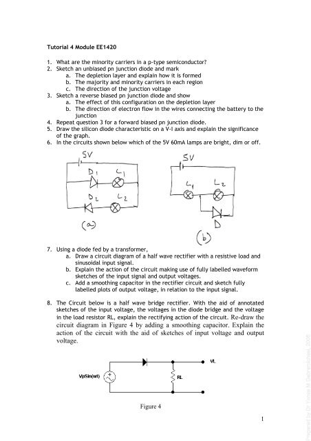
6. In the circuits shown below which of the 5V 60mA lamps are bright, dim or off.<br />
7. Using a diode fed by a transformer,<br />
a. Draw a circuit diagram of a half wave rectifier with a resistive load and<br />
sinusoidal input signal.<br />
b. Explain the <strong>ac</strong>tion of the circuit making use of fully labelled waveform<br />
sketches of the input signal and output voltages.<br />
c. Add a smoothing cap<strong>ac</strong>itor in the rectifier circuit and sketch fully<br />
labelled plots of output voltage, in relation to the input signal.<br />
8. The Circuit below is a half wave bridge rectifier. With the aid of annotated<br />
sketches of the input voltage, the voltages in the diode bridge and the voltage<br />
in the load resistor RL, explain the rectifying <strong>ac</strong>tion of the circuit. Re-draw the<br />
circuit diagram in Figure 4 by adding a smoothing cap<strong>ac</strong>itor. Explain the<br />
<strong>ac</strong>tion of the circuit with the aid of sketches of input voltage and output<br />
voltage.<br />
Figure 4<br />
1<br />
Prepared by Dr Yonas M Gebremichael, 2005
9. The Circuit below is a full wave bridge rectifier. With the aid of annotated<br />
sketches of the input voltage, the voltages in the diode bridge and the voltage<br />
in the load resistor RL, explain the rectifying <strong>ac</strong>tion of the circuit.<br />
2<br />
Prepared by Dr Yonas M Gebremichael, 2005