LT1033 - 3A. Negative Adjustable Regulator - Linear Technology
LT1033 - 3A. Negative Adjustable Regulator - Linear Technology
LT1033 - 3A. Negative Adjustable Regulator - Linear Technology

Create successful ePaper yourself
Turn your PDF publications into a flip-book with our unique Google optimized e-Paper software.
<strong>LT1033</strong><br />
APPLICATIONS INFORMATION<br />
U W U U<br />
larger than 10µF may be used, but if the output is larger<br />
than 25V, a diode, D2, should be added between the output<br />
and adjustment pins (see Figure 2).<br />
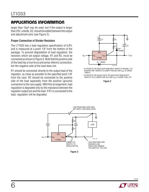
Proper Connection of Divider Resistors<br />
The <strong>LT1033</strong> has a load regulation specification of 0.8%<br />
and is measured at a point 1/8" from the bottom of the<br />
package. To prevent degradation of load regulation, the<br />
resistors which set output voltage, R1 and R2, must be<br />
connected as shown in Figure 3. Note that the positive side<br />
of the load has a true force and sense (Kelvin) connection,<br />
but the negative side of the load does not.<br />
R1 should be connected directly to the output lead of the<br />
regulator, as close as possible to the specified point 1/8"<br />
from the case. R2 should be connected to the positive<br />
side of the load separately from the positive (ground)<br />
connection to the raw supply. With this arrangement, load<br />
regulation is degraded only by the resistance between the<br />
regulator output pin and the load. If R1 is connected to the<br />
load, regulation will be degraded.<br />
ADJ<br />
C1<br />
–V IN V IN V OUT<br />
<strong>LT1033</strong><br />
+<br />
D1* 1N4002<br />
R2<br />
R1<br />
<strong>LT1033</strong> • F02<br />
D2**<br />
1N4002<br />
C3<br />
+<br />
–V OUT<br />
*D1 PROTECTS THE REGULATOR FROM INPUT SHORTS TO GROUND. IT IS<br />
REQUIRED ONLY WHEN C3 IS LARGER THAN 20µF AND V OUT IS LARGER<br />
THAN 6V<br />
** D2 PROTECTS THE ADJUST PIN OF THE REGULATOR FROM OUTPUT<br />
SHORTS IF C2 IS LARGER THAN 10µF AND V OUT IS LARGER THAN –25V<br />
Figure 2<br />
LEAD RESISTANCE HERE DOES<br />
NOT AFFECT LOAD REGULATION<br />
R2<br />
R1<br />
LOAD<br />
ADJ<br />
–V IN V IN V OUT<br />
<strong>LT1033</strong> • F03<br />
<strong>LT1033</strong><br />
CONNECT R1<br />
DIRECTLY TO<br />
REGULATOR PIN<br />
Figure 3<br />
LEAD RESISTANCE HERE<br />
DEGRADES LOAD<br />
REGULATION. MINIMIZE<br />
THE LENGTH OF THIS LEAD<br />
6<br />
1033fc