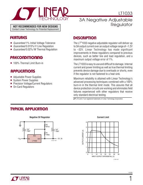
LT1033 - 3A. Negative Adjustable Regulator - Linear Technology
LT1033 - 3A. Negative Adjustable Regulator - Linear Technology
LT1033 - 3A. Negative Adjustable Regulator - Linear Technology

You also want an ePaper? Increase the reach of your titles
YUMPU automatically turns print PDFs into web optimized ePapers that Google loves.
NOT RECOMMENDED FOR NEW DESIGNS<br />
Contact <strong>Linear</strong> <strong>Technology</strong> for Potential Replacement<br />
<strong>LT1033</strong><br />
<strong>3A</strong> <strong>Negative</strong> <strong>Adjustable</strong><br />
<strong>Regulator</strong><br />
FEATURES<br />
■<br />
■<br />
■<br />
■<br />
■<br />
■<br />
■<br />
■<br />
Guaranteed 1% Initial Voltage Tolerance<br />
Guaranteed 0.015%/V Line Regulation<br />
Guaranteed 0.02%/ W Thermal Regulation<br />
PRECO DITIO I G<br />
U<br />
100% Thermal Limit Burn-in<br />
APPLICATIO S<br />
U<br />
U U<br />
<strong>Adjustable</strong> Power Supplies<br />
System Power Supplies<br />
Precision Voltage/Current <strong>Regulator</strong>s<br />
On-Card <strong>Regulator</strong>s<br />
DESCRIPTIO<br />
U<br />
The LT ® 1033 negative adjustable regulator will deliver up<br />
to <strong>3A</strong> output current over an output voltage range of –1.2V<br />
to –32V. <strong>Linear</strong> <strong>Technology</strong> has made significant<br />
improvements in these regulators compared to previous<br />
devices, such as better line and load regulation, and a<br />
maximum output voltage error of 1%.<br />
The <strong>LT1033</strong> is easy to use and difficult to damage. Internal<br />
current and power limiting as well as true thermal limiting<br />
prevents device damage due to overloads or shorts, even<br />
if the regulator is not fastened to a heat sink.<br />
Maximum reliability is attained with <strong>Linear</strong> <strong>Technology</strong>’s<br />
advanced processing techniques combined with a 100%<br />
burn-in in the thermal limit mode. This assures that all<br />
device protection circuits are working and eliminates field<br />
failures experienced with other regulators that receive<br />
only standard electrical testing.<br />
, LTC and LT are registered trademarks of <strong>Linear</strong> <strong>Technology</strong> Corporation.<br />
TYPICAL APPLICATIO<br />
U<br />
<strong>Negative</strong> 5V <strong>Regulator</strong><br />
Current Limit<br />
R2<br />
301Ω<br />
2µF<br />
TANT<br />
R1<br />
100Ω<br />
ADJ<br />
–V IN IN OUT<br />
<strong>LT1033</strong><br />
+ +<br />
<strong>LT1033</strong> • TA01<br />
2µF<br />
TANT<br />
–5V, <strong>3A</strong><br />
OUTPUT CURRENT (A)<br />
6<br />
5<br />
4<br />
3<br />
2<br />
1<br />
0<br />
0 5 10 15 20 25 30 35<br />
INPUT-OUTPUT DIFFERENTIAL (V)<br />
<strong>LT1033</strong> • G01<br />
1033fc<br />
1
<strong>LT1033</strong><br />
ABSOLUTE AXI U RATI GS<br />
W W W<br />
(Note 1)<br />
Power Dissipation....................................... Internally Limited<br />
Input to Output Voltage Differential ................................. 35V<br />
Operating Junction Temperature Range<br />
<strong>LT1033</strong>M (OBSOLETE) ............................... –55°C to 150°C<br />
<strong>LT1033</strong>C ......................................................... 0°C to 125°C<br />
U<br />
Storage Temperature Range<br />
<strong>LT1033</strong>M (OBSOLETE) ............................... –65°C to 150°C<br />
<strong>LT1033</strong>C ..................................................... –65°C to 150°C<br />
Lead Temperature (Soldering, 10 sec.) ........................ 300°C<br />
U U W<br />
PACKAGE/ORDER I FOR ATIO<br />
BOTTOM VIEW<br />
FRONT VIEW<br />
FRONT VIEW<br />
1 2<br />
ADJ V OUT<br />
CASE IS<br />
V IN<br />
K PACKAGE<br />
4-LEAD TO-3 METAL CAN<br />
T JMAX = 150°C, θ JA = 35°C/W(MK)<br />
T JMAX = 125°C, θ JA = 35°C/W(CK)<br />
OBSOLETE PACKAGE<br />
Consider the P or T Packages for Alternate Source<br />
ORDER PART NUMBER<br />
<strong>LT1033</strong>MK<br />
<strong>LT1033</strong>CK<br />
CASE IS V IN<br />
T PACKAGE<br />
3-LEAD PLASTIC TO-220<br />
T JMAX = 125°C, θ JA = 50°C/W<br />
V OUT<br />
V IN<br />
ADJ<br />
ORDER PART NUMBER<br />
<strong>LT1033</strong>CT<br />
V IN<br />
CASE IS V IN<br />
P PACKAGE<br />
3-LEAD PLASTIC TO-3P<br />
T JMAX = 125°C, θ JA = 35°C/W<br />
ORDER PART NUMBER<br />
<strong>LT1033</strong>CP<br />
V OUT<br />
ADJ<br />
Consult LTC Marketing for parts specified with wider operating temperature ranges.<br />
ELECTRICAL CHARACTERISTICS<br />
(Note 2)<br />
The ● denotes specifications which apply over the full operating temperature range, otherwise specifications are T A = 25°C.<br />
<strong>LT1033</strong>M<br />
<strong>LT1033</strong>C<br />
SYMBOL PARAMETER CONDITIONS MIN TYP MAX MIN TYP MAX UNITS<br />
V REF Reference Voltage |V IN – V OUT | = 5V, I OUT = 5mA,<br />
T J = 25°C –1.238 –1.250 –1.262 –1.238 –1.250 –1.262 V<br />
2<br />
3V ≤ |V IN – V OUT | ≤ 35V<br />
5mA ≤ I OUT ≤␣I MAX , P ≤ P MAX ● –1.215 –1.250 –1.285 –1.200 –1.250 –1.300 V<br />
∆V OUT Load Regulation 10mA ≤ I OUT ≤ I MAX , (Note 3)<br />
∆I OUT T J = 25°C,|V OUT | ≤ 5V 10 50 10 50 mV<br />
T J = 25°C,|V OUT | ≥ 5V 0.2 1.0 0.2 1.0 %<br />
|V OUT | ≤ 5V ● 20 75 20 75 mV<br />
|V OUT | ≥ 5V ● 0.4 1.5 0.4 1.5 %<br />
∆V OUT Line Regulation 3V ≤ |V IN – V OUT | ≤ 35V, (Note 2)<br />
∆V IN T J = 25°C 0.005 0.015 0.01 0.02 %/V<br />
● 0.01 0.04 0.02 0.05 %/V<br />
Ripple Rejection<br />
V OUT = –10V, f = 120Hz<br />
C ADJ = 0 56 66 60 dB<br />
C ADJ = 10µF 70 80 66 77 dB<br />
Thermal Regulation T J = 25°C, 10ms Pulse 0.002 0.02 0.002 0.02 %/W<br />
1033fc
ELECTRICAL CHARACTERISTICS<br />
(Note 2)<br />
The ● denotes specifications which apply over the full operating temperature range, otherwise specifications are T A = 25°C.<br />
<strong>LT1033</strong><br />
<strong>LT1033</strong>M<br />
<strong>LT1033</strong>C<br />
SYMBOL PARAMETER CONDITIONS MIN TYP MAX MIN TYP MAX UNITS<br />
I ADJ Adjust Pin Current ● 65 100 65 100 µA<br />
∆I ADJ Adjust Pin Current Change 10mA ≤␣I OUT ≤ I MAX ● 0.2 2 0.5 2 µA<br />
3V ≤ |V IN – V OUT | ≤ 35V ● 1.0 5 2 5 µA<br />
Minimum Load Current |V IN – V OUT | ≤ 35V 2.5 5.0 2.5 5.0 mA<br />
|V IN – V OUT | ≤ 10V 1.2 3.0 1.2 3.0 mA<br />
I SC Current Limit |V IN – V OUT | ≤ 10V, (Note 3) 3 4.3 6 3 4.3 6 A<br />
|V IN – V OUT | = 35V, T J = 25°C 0.5 1.3 2.5 0.5 1.3 2.5 A<br />
∆V OUT Temperature Stability of T MIN ≤ T ≤ T MAX ● 0.6 1.5 0.6 1.5 %<br />
∆Temp Output Voltage<br />
∆V OUT Long Term Stability T A = 125°C, 1000 Hours 0.3 1.0 0.3 1.0 %<br />
∆Time<br />
e n RMS Output Noise T A = 25°C, 10Hz ≤ f ≤ 10kHz 0.003 0.003 %<br />
(% of V OUT )<br />
θ JC Thermal Resistance T Package 2.5 4.0 °C/W<br />
Junction to Case K Package 1.2 2.0 1.2 2.0 °C/W<br />
P Package 1.8 2.7 °C/W<br />
Note 1: Absolute Maximum Ratings are those values beyond which the life<br />
of a device may be impaired.<br />
Note 2: Unless otherwise indicated, these specifications apply:<br />
|V IN – V OUT | = 5V; and I OUT = 5mA. Power dissipation is internally limited.<br />
However, these specifications apply for power dissipation up to 30W.<br />
See guaranteed minimum output current curve. I MAX = <strong>3A</strong>.<br />
Note 3: Testing is done using a pulsed low duty cycle technique. See<br />
thermal regulation specifications for output changes due to heating effects.<br />
Load regulation is measured on the output pin at a point 1/8" below the<br />
base of the package.<br />
TYPICAL PERFOR A CE CHARACTERISTICS<br />
UW<br />
2.8<br />
Dropout Voltage<br />
1.27<br />
Temperature Stability<br />
1.8<br />
Minimum Load Current<br />
INPUT-OUTPUT DIFFERENTIAL (V)<br />
2.6<br />
2.4<br />
2.2<br />
2.0<br />
1.8<br />
1.6<br />
1.4<br />
T J = –55°C<br />
T J = 25°C<br />
T J = 150°C<br />
REFERENCE VOLTAGE (V)<br />
1.26<br />
1.25<br />
1.24<br />
CURRENT (mA)<br />
1.6<br />
1.4<br />
1.2<br />
1.0<br />
0.8<br />
0.6<br />
0.4<br />
0.2<br />
T J = 150°C<br />
T J = –55°C<br />
T J = 25°C<br />
1.2<br />
0.5 1.0 1.5 2.0 2.5 3.0<br />
OUTPUT CURRENT (A)<br />
1.23<br />
–75 –50 –25 0 25 50 75 100 125 150<br />
TEMPERATURE (°C)<br />
0<br />
0 10 20 30 40<br />
INPUT-OUTPUT DIFFERENTIAL (V)<br />
<strong>LT1033</strong> • G02<br />
<strong>LT1033</strong> • G03<br />
<strong>LT1033</strong> • G04<br />
1033fc<br />
3
<strong>LT1033</strong><br />
TYPICAL PERFORMANCE CHARACTERISTICS<br />
U W<br />
Ripple Rejection Ripple Rejection Ripple Rejection<br />
100<br />
100<br />
100<br />
RIPPLE REJECTION (dB)<br />
80<br />
60<br />
40<br />
C ADJ = 10µF<br />
C ADJ = 0<br />
V IN – V OUT = 5V<br />
20 I L = 500mA<br />
f = 120Hz<br />
T J = 25°C<br />
0<br />
0 –10 –20 –30 –40<br />
OUTPUT VOLTAGE (V)<br />
RIPPLE REJECTION (dB)<br />
80<br />
60<br />
40<br />
C ADJ = 0<br />
C ADJ = 10µF<br />
V IN = –15V<br />
20 V OUT = –10V<br />
I L = 500mA<br />
T J = 25°C<br />
0<br />
10 100 1k 10k 100k 1M<br />
FREQUENCY (Hz)<br />
RIPPLE REJECTION (dB)<br />
80<br />
60<br />
40<br />
C ADJ = 10µF<br />
C ADJ = 0<br />
V IN = –15V<br />
20 V OUT = –10V<br />
f = 120Hz<br />
T J = 25°C<br />
0<br />
0.01 0.1 1 10<br />
OUTPUT CURRENT (A)<br />
<strong>LT1033</strong> • G05<br />
<strong>LT1033</strong> • G06<br />
<strong>LT1033</strong> • G07<br />
OUTPUT IMPEDANCE (Ω)<br />
101<br />
100<br />
10 –1<br />
10–2<br />
Output Impedance Line Transient Response Load Transient Response<br />
V IN = –15V<br />
V OUT = –10V<br />
I L = 500mA<br />
C L = 1µF<br />
T J = 25°C<br />
C ADJ = 0<br />
C ADJ = 10µF<br />
10–3<br />
10 100 1k 10k 100k 1M<br />
FREQUENCY (Hz)<br />
OUTPUT VOLTAGE<br />
DEVIATION (V)<br />
INPUT VOLTAGE<br />
CHANGE (V)<br />
0.8<br />
0.6<br />
0.4<br />
0.2<br />
0<br />
–0.2<br />
–0.4<br />
0<br />
–0.5<br />
–1.0<br />
C ADJ = 0<br />
C ADJ = 10µF<br />
V OUT = –10V<br />
I L = 50mA<br />
T J = 25°C<br />
C L = 1µF<br />
0 10 20<br />
TIME (µs)<br />
30 40<br />
OUTPUT VOLTAGE<br />
DEVIATION (V)<br />
LOAD CURRENT (A)<br />
0.6<br />
0.4<br />
0.2<br />
0<br />
–0.2<br />
–0.4<br />
–0.6<br />
0<br />
–0.5<br />
–1.0<br />
–1.5<br />
C ADJ = 0<br />
C ADJ = 10µF<br />
V IN = –15V<br />
V OUT = –10V<br />
I NL = 50mA<br />
T J = 25°C<br />
C L = 1µF<br />
0 10 20<br />
TIME (µs)<br />
30 40<br />
<strong>LT1033</strong> • G08<br />
<strong>LT1033</strong> • G09<br />
<strong>LT1033</strong> • G10<br />
Load Regulation*<br />
Guaranteed Minimum<br />
Output Current<br />
Adjustment Current<br />
OUTPUT VOLTAGE DEVIATION (%)<br />
0.8<br />
0.4<br />
0<br />
–0.4<br />
–0.8<br />
OUTPUT CURRENT (A)<br />
5<br />
4<br />
3<br />
2<br />
1<br />
ADJUSTMENT CURRENT (µA)<br />
80<br />
75<br />
70<br />
65<br />
60<br />
55<br />
0 0.8 1.6 2.4 3.2 4.0<br />
OUTPUT CURRENT (A)<br />
*THE <strong>LT1033</strong> HAS LOAD REGULATION COMPENSATION<br />
WHICH MAKES THE TYPICAL UNIT READ CLOSE TO ZERO.<br />
THIS BAND REPRESENTS THE TYPICAL PRODUCTION SPREAD<br />
0<br />
0 5 10 15 20 25 30 35<br />
INPUT-OUTPUT DIFFERENTIAL (V)<br />
<strong>LT1033</strong> • G12<br />
50<br />
–75 –50 –25 0 25 50 75 100 125 150<br />
TEMPERATURE (°C)<br />
<strong>LT1033</strong> • G13<br />
<strong>LT1033</strong> • G11<br />
4<br />
1033fc
<strong>LT1033</strong><br />
APPLICATIONS INFORMATION<br />
Output Voltage<br />
The output voltage is determined by two external resistors,<br />
R1 and R2 (see Figure 1). The exact formula for the<br />
output voltage is:<br />
V<br />
⎛ R2⎞<br />
= V ⎜1+<br />
⎟ + I ( R2)<br />
⎝ R1⎠<br />
OUT REF ADJ<br />
Where: V REF = Reference Voltage, I ADJ = Adjustment Pin<br />
Current. In most applications, the second term is small<br />
enough to be ignored, typically about 0.5% of V OUT . In<br />
more critical applications, the exact formula should be<br />
used, with I ADJ equal to 65µA. Solving for R2 yields:<br />
VOUT<br />
– V<br />
R2<br />
=<br />
VREF<br />
– I<br />
R1<br />
+<br />
C1<br />
R2<br />
10µF<br />
I ADJ<br />
C3<br />
C2<br />
2µF<br />
5µF<br />
V REF R1<br />
ADJ<br />
–V IN V IN V OUT –V OUT<br />
<strong>LT1033</strong><br />
<strong>LT1033</strong> • F01<br />
EXAMPLE:<br />
1. A PRECISION 10V REGULATOR TO SUPPLY UP TO <strong>3A</strong> LOAD CURRENT.<br />
A. SELECT R1 = 100Ω TO MINIMIZE EFFECT OF I ADJ<br />
B. CALCULATE R2 = V OUT – V REF 10V – 1.25V<br />
= = 704Ω<br />
V REF 1.25V<br />
– I<br />
R1 ADJ<br />
100Ω – 65µA<br />
+<br />
+<br />
REF<br />
ADJ<br />
U W U U<br />
Smaller values of R1 and R2 will reduce the influence of<br />
I ADJ on the output voltage, but the no-load current drain on<br />
the regulator will be increased. Typical values for R1 are<br />
between 100Ω and 300Ω, giving 12.5mA and 4.2mA<br />
no-load current respectively. There is an additional consideration<br />
in selecting R1, the minimum load current<br />
specification of the regulator. The operating current of the<br />
<strong>LT1033</strong> flows from input to output. If this current is not<br />
absorbed by the load, the output of the regulator will rise<br />
above the regulated value. The current drawn by R1 and R2<br />
is normally high enough to absorb the current, but care<br />
must be taken in no-load situations where R1 and R2 have<br />
high values. The maximum value for the operating current,<br />
Figure 1<br />
which must be absorbed, is 5mA for the <strong>LT1033</strong>. If inputoutput<br />
voltage differential is less than 10V, the operating<br />
current that must be absorbed drops to 3mA.<br />
Capacitors and Protection Diodes<br />
An output capacitor, C3, is required to provide proper<br />
frequency compensation of the regulator feedback loop.<br />
A 2µF or larger solid tantalum capacitor is generally<br />
sufficient for this purpose if the 1MHz impedance of the<br />
capacitor is 1Ω or less. High Q capacitors, such as Mylar,<br />
are not recommended because their extremely low ESR<br />
(effective series resistance) can drastically reduce phase<br />
margin. When these types of capacitors must be used<br />
because of other considerations, add a 0.5Ω carbon<br />
resistor in series with 1µF. Aluminum electrolytic capacitors<br />
may be used, but the minimum value should be 25µF<br />
to ensure a low impedance at 1MHz. The output capacitor<br />
should be located within a few inches of the regulator to<br />
keep lead impedance to a minimum. The following caution<br />
should be noted: if the output voltage is greater than 6V<br />
and an output capacitor greater than 20µF has been used,<br />
it is possible to damage the regulator if the input voltage<br />
becomes shorted, due to the output capacitor discharging<br />
into the regulator. This can be prevented by using diode D1<br />
(see Figure 2) between the input and the output.<br />
The input capacitor, C2, is only required if the regulator is<br />
more than 4 inches from the raw supply filter capacitor.<br />
Bypassing the Adjustment Pin<br />
The adjustment pin of the <strong>LT1033</strong> may be bypassed with<br />
a capacitor to ground, C1, to reduce output ripple, noise,<br />
and impedance. These parameters scale directly with<br />
output voltage if the adjustment pin is not bypassed. A<br />
bypass capacitor reduces ripple, noise and impedance to<br />
that of a 1.25V regulator. In a 15V regulator for example,<br />
these parameters are improved by 15V/1.25V = 12 to 1.<br />
This improvement holds only for those frequencies where<br />
the impedance of the bypass capacitor is less than R1. Ten<br />
microfarads is generally sufficient for 60Hz power line<br />
applications where the ripple frequency is 120Hz, since<br />
X C = 130Ω. The capacitor should have a voltage rating at<br />
least as high as the output voltage of the regulator. Values<br />
1033fc<br />
5
<strong>LT1033</strong><br />
APPLICATIONS INFORMATION<br />
U W U U<br />
larger than 10µF may be used, but if the output is larger<br />
than 25V, a diode, D2, should be added between the output<br />
and adjustment pins (see Figure 2).<br />
Proper Connection of Divider Resistors<br />
The <strong>LT1033</strong> has a load regulation specification of 0.8%<br />
and is measured at a point 1/8" from the bottom of the<br />
package. To prevent degradation of load regulation, the<br />
resistors which set output voltage, R1 and R2, must be<br />
connected as shown in Figure 3. Note that the positive side<br />
of the load has a true force and sense (Kelvin) connection,<br />
but the negative side of the load does not.<br />
R1 should be connected directly to the output lead of the<br />
regulator, as close as possible to the specified point 1/8"<br />
from the case. R2 should be connected to the positive<br />
side of the load separately from the positive (ground)<br />
connection to the raw supply. With this arrangement, load<br />
regulation is degraded only by the resistance between the<br />
regulator output pin and the load. If R1 is connected to the<br />
load, regulation will be degraded.<br />
ADJ<br />
C1<br />
–V IN V IN V OUT<br />
<strong>LT1033</strong><br />
+<br />
D1* 1N4002<br />
R2<br />
R1<br />
<strong>LT1033</strong> • F02<br />
D2**<br />
1N4002<br />
C3<br />
+<br />
–V OUT<br />
*D1 PROTECTS THE REGULATOR FROM INPUT SHORTS TO GROUND. IT IS<br />
REQUIRED ONLY WHEN C3 IS LARGER THAN 20µF AND V OUT IS LARGER<br />
THAN 6V<br />
** D2 PROTECTS THE ADJUST PIN OF THE REGULATOR FROM OUTPUT<br />
SHORTS IF C2 IS LARGER THAN 10µF AND V OUT IS LARGER THAN –25V<br />
Figure 2<br />
LEAD RESISTANCE HERE DOES<br />
NOT AFFECT LOAD REGULATION<br />
R2<br />
R1<br />
LOAD<br />
ADJ<br />
–V IN V IN V OUT<br />
<strong>LT1033</strong> • F03<br />
<strong>LT1033</strong><br />
CONNECT R1<br />
DIRECTLY TO<br />
REGULATOR PIN<br />
Figure 3<br />
LEAD RESISTANCE HERE<br />
DEGRADES LOAD<br />
REGULATION. MINIMIZE<br />
THE LENGTH OF THIS LEAD<br />
6<br />
1033fc
+<br />
<strong>LT1033</strong><br />
TYPICAL APPLICATIO S<br />
The output stability, load regulation, line regulation,<br />
thermal regulation, temperature drift, long term drift, and<br />
noise can be improved by a factor of 6.6 over the standard<br />
regulator configuration. This assumes a zener whose drift<br />
and noise is considerably better than the regulator itself.<br />
The LM329B has 20ppm/°C maximum drift and about 10<br />
times lower noise than the regulator.<br />
In the application shown below, regulators #2 to “N” will<br />
track regulator #1 to within ±24mV initially, and to ±60mV<br />
over all load, line, and temperature conditions. If any<br />
regulator output is shorted to ground, all other outputs will<br />
drop to ≈ –2V. Load regulation of regulators #2 to “N” will<br />
be improved by V OUT /1.25V compared to a standard<br />
regulator, so regulator #1 should be the one which has the<br />
lowest load current.<br />
Multiple Tracking <strong>Regulator</strong>s<br />
C1<br />
2µF<br />
–V IN V IN REG #1 V OUT<br />
–V OUT1<br />
2µF<br />
1N4002 R1 SOLID<br />
ADJ<br />
120Ω TANTALUM<br />
2µF<br />
V IN<br />
<strong>LT1033</strong><br />
ADJ<br />
REG #2 V OUT<br />
<strong>LT1033</strong><br />
C3<br />
10µF<br />
1N4002<br />
+<br />
+<br />
R2<br />
+<br />
+<br />
U<br />
2µF<br />
SOLID<br />
TANTALUM<br />
–V OUT2<br />
+<br />
ADJ<br />
High Stability <strong>Regulator</strong><br />
7V<br />
LM329B<br />
R3<br />
1.5k<br />
1%<br />
R2*<br />
R1<br />
1k<br />
1%<br />
–V IN V IN V OUT –V OUT<br />
<strong>LT1033</strong><br />
|V OUT |<br />
*R2 = – 908Ω<br />
9.08 • 10 –3<br />
<strong>LT1033</strong> • TA06<br />
Dual Tracking <strong>3A</strong> Supply ± 1.25V to ± 20V<br />
1µF<br />
SOLID<br />
TANTALUM<br />
V IN V OUT<br />
+<br />
LT150A<br />
+V IN<br />
+V OUT<br />
ADJ<br />
R1**<br />
100Ω<br />
1% 2.2µF* D1<br />
–V IN V IN V OUT<br />
–V OUT<br />
1N4002<br />
+ R2<br />
10µF 5k<br />
1%<br />
R3<br />
5k<br />
+ R4<br />
10µF 5k<br />
1%<br />
R5** +<br />
2.2µF* D2<br />
100Ω<br />
1N4002<br />
1%<br />
ADJ<br />
<strong>LT1033</strong><br />
<strong>LT1033</strong> • TA07<br />
*SOLID TANTALUM<br />
**R1 OR R5 MAY BE TRIMMED SLIGHTLY TO IMPROVE TRACKING<br />
+<br />
2µF<br />
V IN V OUT<br />
2µF<br />
ADJ<br />
SOLID<br />
TANTALUM<br />
REG #N<br />
–V OUT3<br />
<strong>LT1033</strong><br />
<strong>LT1033</strong> • TA05<br />
+<br />
Current <strong>Regulator</strong><br />
(–)<br />
ADJ<br />
<strong>LT1033</strong><br />
+<br />
C1<br />
2µF<br />
SOLID TANTALUM<br />
V IN V OUT<br />
<strong>LT1033</strong> • TA08<br />
R S I<br />
(+)<br />
1.25V<br />
(O.5Ω ≤ R S ≤ 250Ω) I = 65µA +<br />
R S<br />
1033fc<br />
7
8<br />
<strong>LT1033</strong><br />
1033fc<br />
600Ω<br />
Q16<br />
Q31<br />
V IN<br />
V OUT<br />
ADJ<br />
2k<br />
2k<br />
D4<br />
D3<br />
D5<br />
D2<br />
D1<br />
5k<br />
100k<br />
60k<br />
750Ω<br />
2k<br />
15pF<br />
20k<br />
15pF<br />
18k<br />
600Ω<br />
25pF<br />
800Ω<br />
20Ω<br />
20Ω<br />
100k<br />
220Ω<br />
5pF<br />
2pF<br />
20k<br />
4.2k 4k<br />
8k<br />
1k<br />
4k<br />
1k 2.4k<br />
6.8k<br />
500Ω<br />
250Ω<br />
0.02Ω<br />
100Ω<br />
100Ω<br />
460Ω<br />
12k<br />
12k<br />
10Ω<br />
150Ω<br />
15k<br />
6k<br />
2k<br />
12k<br />
270Ω<br />
Q7<br />
<strong>LT1033</strong> • SC01<br />
1k<br />
Q8<br />
Q1<br />
Q3<br />
Q4<br />
Q2<br />
Q32<br />
Q34<br />
Q33<br />
Q9<br />
Q10<br />
Q12<br />
Q11<br />
Q25<br />
Q24<br />
Q22<br />
Q23<br />
Q27<br />
Q28<br />
Q30<br />
Q21<br />
Q19<br />
Q20<br />
Q17<br />
Q15<br />
Q18<br />
Q14<br />
Q13<br />
Q6<br />
Q26<br />
Q29<br />
SCHE ATIC DIAGRA<br />
W<br />
W
<strong>LT1033</strong><br />
PROGRAM RESISTOR SELECTIO<br />
U W<br />
The following table allows convenient selection of<br />
program resistors from standard 1% values.<br />
OUTPUT ERROR<br />
V OUT R1 R2 (%)<br />
5 100 301 0.6<br />
6 121 453 –0.7<br />
8 115 619 0.6<br />
10 115 806 0.6<br />
12 118 1020 1.0<br />
15 100 1100 0.5<br />
18 150 2000 0.2<br />
20 121 1820 0.8<br />
22 130 2150 0.2<br />
24 121 2210 0.9<br />
28 115 2430 –0.7<br />
30 121 2740 –0.9<br />
PACKAGE DESCRIPTION<br />
U<br />
K Package<br />
2-Lead TO-3 Metal Can<br />
(Reference LTC DWG # 05-08-1310)<br />
0.320 – 0.350<br />
(8.13 – 8.89)<br />
0.760 – 0.775<br />
(19.30 – 19.69)<br />
0.060 – 0.135<br />
(1.524 – 3.429)<br />
0.420 – 0.480<br />
(10.67 – 12.19)<br />
0.038 – 0.043<br />
(0.965 – 1.09)<br />
0.210 – 0.220<br />
(5.33 – 5.59)<br />
1.177 – 1.197<br />
(29.90 – 30.40)<br />
0.655 – 0.675<br />
(16.64 – 17.15)<br />
0.151 – 0.161<br />
(3.86 – 4.09)<br />
DIA, 2PLCS<br />
0.167 – 0.177<br />
(4.24 – 4.49)<br />
0.425 – 0.435<br />
R<br />
(10.80 – 11.05) OBSOLETE<br />
0.067 – 0.077<br />
0.490 – 0.510<br />
(1.70 – 1.96)<br />
(12.45 – 12.95)<br />
PACKAGE<br />
R<br />
K2 (TO-3) 1098<br />
1033fc<br />
9
<strong>LT1033</strong><br />
PACKAGE DESCRIPTION<br />
U<br />
T Package<br />
3-Lead Plastic TO-220<br />
(Reference LTC DWG # 05-08-1420)<br />
0.390 – 0.415<br />
(9.906 – 10.541)<br />
0.147 – 0.155<br />
(3.734 – 3.937)<br />
DIA<br />
0.165 – 0.180<br />
(4.191 – 4.572)<br />
0.045 – 0.055<br />
(1.143 – 1.397)<br />
0.230 – 0.270<br />
(5.842 – 6.858)<br />
0.460 – 0.500<br />
(11.684 – 12.700)<br />
0.330 – 0.370<br />
(8.382 – 9.398)<br />
0.570 – 0.620<br />
(14.478 – 15.748)<br />
0.980 – 1.070<br />
(24.892 – 27.178)<br />
0.520 – 0.570<br />
(13.208 – 14.478)<br />
0.218 – 0.252<br />
(5.537 – 6.401)<br />
0.100<br />
(2.540)<br />
BSC<br />
0.013 – 0.023<br />
(0.330 – 0.584)<br />
0.095 – 0.115<br />
0.050<br />
(2.413 – 2.921)<br />
0.028 – 0.038<br />
(1.270)<br />
(0.711 – 0.965) TYP<br />
T3 (TO-220) 1098<br />
10<br />
1033fc
<strong>LT1033</strong><br />
PACKAGE DESCRIPTION<br />
U<br />
P Package<br />
3-Lead Plastic TO-3P (Similar to TO-247)<br />
(Reference LTC DWG # 05-08-1450)<br />
0.560<br />
(14.224)<br />
0.325<br />
(8.255)<br />
0.275<br />
(6.985)<br />
0.620 – 0.64O<br />
(15.75 – 16.26)<br />
MOUNTING HOLE<br />
0.115 – 0.145<br />
(2.92 – 3.68)<br />
DIA<br />
18° – 22°<br />
0.187 – 0.207<br />
(4.75 – 5.26)<br />
0.060 – 0.080<br />
(1.52 – 2.03)<br />
0.580<br />
(14.732)<br />
0.700<br />
(17.780)<br />
0.830 – 0.870<br />
(21.08 – 22.10)<br />
0.580 – 0.6OO<br />
(14.73 – 15.24)<br />
0.170 – 0.2OO<br />
(4.32 – 5.08)<br />
EJECTOR PIN MARKS<br />
0.105 – 0.125<br />
(2.67 – 3.18)<br />
DIA<br />
0.098<br />
(2.489)<br />
0.124<br />
(3.149)<br />
0.780 – 0.800<br />
(19.81 – 20.32)<br />
0.170<br />
(4.32)<br />
MAX<br />
3° – 7°<br />
BOTTOM VIEW OF TO-3P<br />
HATCHED AREA IS SOLDER PLATED<br />
COPPER HEAT SINK<br />
0.042 – 0.052<br />
(1.07 – 1.32)<br />
0.074 – 0.084<br />
(1.88 – 2.13)<br />
0.215<br />
(5.46)<br />
BSC<br />
0.113 – 0.123<br />
(2.87 – 3.12)<br />
0.087 – 0.102<br />
(2.21 – 2.59)<br />
0.020 – 0.040<br />
(0.51 – 1.02)<br />
P3 0996<br />
Information furnished by <strong>Linear</strong> <strong>Technology</strong> Corporation is believed to be accurate and reliable.<br />
However, no responsibility is assumed for its use. <strong>Linear</strong> <strong>Technology</strong> Corporation makes no representation<br />
that the interconnection of its circuits as described herein will not infringe on existing patent rights.<br />
1033fc<br />
11
<strong>LT1033</strong><br />
RELATED PARTS<br />
PART NUMBER DESCRIPTION COMMENTS<br />
LT1120 125mA Low Dropout <strong>Regulator</strong> with 20µA I Q Includes 2.5V Reference and Comparator<br />
LT1121 150mA Micropower Low Dropout <strong>Regulator</strong> 30µA I Q , SOT-223 Package<br />
LT1129 700mA Micropower Low Dropout <strong>Regulator</strong> 50µA Quiescent Current<br />
LT1175 500mA <strong>Negative</strong> Low Dropout Micropower <strong>Regulator</strong> 45µA I Q , 0.26V Dropout Voltage, SOT-223 Package<br />
LT1374 4.5A, 500kHz Step-Down Converter 4.5A, 0.07Ω Internal Switch, SO-8 Package<br />
LT1521 300mA Low Dropout Micropower <strong>Regulator</strong> with Shutdown 15µA I Q , Reverse Battery Protection<br />
LT1529 <strong>3A</strong> Low Dropout <strong>Regulator</strong> with 50µA I Q 500mV Dropout Voltage<br />
LT1573 UltraFast Transient Response Low Dropout <strong>Regulator</strong> Drives External PNP<br />
LT1575 UltraFast Transient Response Low Dropout <strong>Regulator</strong> Drives External N-Channel MOSFET<br />
LT1735 Synchronous Step-Down Converter High Efficiency, OPTI-LOOP ® Compensation<br />
LT1761 Series 100mA, Low Noise, Low Dropout Micropower <strong>Regulator</strong>s in SOT-23 20µA Quiescent Current, 20µV RMS Noise, SOT-23 Package<br />
LT1762 Series 150mA, Low Noise, LDO Micropower <strong>Regulator</strong>s 25µA Quiescent Current, 20µV RMS Noise, MSOP Package<br />
LT1763 Series 500mA, Low Noise, LDO Micropower <strong>Regulator</strong>s 30µA Quiescent Current, 20µV RMS Noise, SO-8 Package<br />
LT1764 <strong>3A</strong>, Low Noise, Fast Transient Response LDO 40µV RMS Noise<br />
LT1962 300mA, Low Noise, LDO Micropower <strong>Regulator</strong> 20µV RMS Noise, MSOP Package<br />
LT1963 1.5A, Low Noise, Fast Transient Response LDO 40µV RMS Noise, SOT-223 Package<br />
OPTI-LOOP is a registered trademark of <strong>Linear</strong> <strong>Technology</strong> Corporation. UltraFast is a trademark of <strong>Linear</strong> <strong>Technology</strong> Corporation.<br />
12<br />
<strong>Linear</strong> <strong>Technology</strong> Corporation<br />
1630 McCarthy Blvd., Milpitas, CA 95035-7417<br />
(408) 432-1900 ● FAX: (408) 434-0507 ● www.linear.com<br />
1033fc<br />
LT/CPI 0102 1.5K REV C • PRINTED IN USA<br />
© LINEAR TECHNOLOGY CORPORATION 1991