PWM and PFM Operation of DC/DC Converters ... - next!-Community
PWM and PFM Operation of DC/DC Converters ... - next!-Community
PWM and PFM Operation of DC/DC Converters ... - next!-Community

Create successful ePaper yourself
Turn your PDF publications into a flip-book with our unique Google optimized e-Paper software.
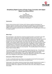
Fig. 7 is a block diagram <strong>of</strong> the TPS61042<br />
boost converter. Note that this device does not<br />
have an internal oscillator. As discussed earlier, a<br />
conventional <strong>PWM</strong> converter uses its clock to<br />
generate a drive signal to the power FETs. (This<br />
drive signal may be gated <strong>of</strong>f or further controlled<br />
by several other factors, as described in the<br />
references listed at the end <strong>of</strong> this topic.)<br />
The TPS61042 shown in Fig. 7 uses<br />
hysteretic-converter architecture that operates in a<br />
different manner. As previously mentioned, this<br />
architecture is sometimes called a “bang-bang<br />
controller.” In this circuit, the main power switch,<br />
Q1, is turned on until a fixed peak current is<br />
reached. When the switch is turned on, the<br />
inductor current begins to increase. The ramp time<br />
to reach the peak threshold limit is dependent on<br />
the inductor value, L, <strong>and</strong> the other operating<br />
conditions <strong>of</strong> the circuit. Once the peak current is<br />
reached, the switch is turned <strong>of</strong>f <strong>and</strong> the energy is<br />
transferred to the output as in any boost converter.<br />
The switch is turned on again when the feedback<br />
pin (FB), or sense voltage, falls below the internal<br />
reference point.<br />
This type <strong>of</strong> converter therefore essentially<br />
self-oscillates based on the measurement <strong>of</strong> the<br />
FB voltage <strong>and</strong> the internal switch current. The<br />
power FET is turned on when required (i.e., when<br />
the FB voltage has fallen below the limit,<br />
typically 250 mV) <strong>and</strong> then turned <strong>of</strong>f when the<br />
internal peak current has reached the upper limit<br />
(typically 500 mA). Because the FB voltage is<br />
affected by the load conditions, <strong>and</strong> the ramp time<br />
is affected by the inductor value <strong>and</strong> the input<br />
voltage, it follows that the effective frequency <strong>of</strong><br />
oscillation will be a function <strong>of</strong> all <strong>of</strong> these<br />
parameters.<br />
This architecture inherently results in some<br />
small amount <strong>of</strong> ripple in the output voltage, since<br />
the power FET is controlled based on FB sagging<br />
below the reference. For applications such as LED<br />
backlight drivers, a small amount <strong>of</strong> ripple does<br />
not visibly affect the LED brightness. For<br />
applications that require very low-ripple output<br />
voltages, a second-stage filter or linear postregulator<br />
(LDO) is sometimes used after the<br />
output section <strong>of</strong> a hysteretic converter.<br />
EN<br />
EN<br />
VREF<br />
0.252 V<br />
SW<br />
Topic 7<br />
V IN<br />
CTRL<br />
GND<br />
UVLO<br />
Bias<br />
Thermal<br />
Shutdown<br />
Enable<br />
Control<br />
Logic<br />
<strong>PWM</strong><br />
Gate<br />
Drive<br />
EN<br />
Control<br />
Logic<br />
Gate<br />
Driver<br />
Current-<br />
Limit<br />
S<strong>of</strong>tstart<br />
6-µs<br />
Maximum<br />
On Time<br />
Overvoltage +<br />
Protection<br />
Q1<br />
R1<br />
2 MΩ<br />
R2<br />
30 kΩ<br />
OVP<br />
Error<br />
Comparator<br />
–<br />
0.4 V<br />
LED<br />
FB<br />
V REF<br />
+<br />
–<br />
400-ns Minimum<br />
Off Time<br />
Q2<br />
RS<br />
Fig. 7. Functional block diagram <strong>of</strong> TPS61042 boost converter.