Design of a 3Bit 20GS/s ADC in 65nm CMOS
Design of a 3Bit 20GS/s ADC in 65nm CMOS
Design of a 3Bit 20GS/s ADC in 65nm CMOS

Create successful ePaper yourself
Turn your PDF publications into a flip-book with our unique Google optimized e-Paper software.
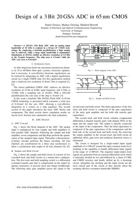
<strong>Design</strong> <strong>of</strong> a 3 Bit 20 GS/s <strong>ADC</strong> <strong>in</strong> 65 nm <strong>CMOS</strong><br />
Damir Ferenci, Markus Gröz<strong>in</strong>g, Manfred Berroth<br />
Institute <strong>of</strong> Electrical and Optical Communications Eng<strong>in</strong>eer<strong>in</strong>g<br />
University <strong>of</strong> Stuttgart<br />
Stuttgart, Germany<br />
damir.ferenci@<strong>in</strong>t.uni-stuttgart.de<br />
Abstract— A 20 GS/s 3 bit flash <strong>ADC</strong> with an analog <strong>in</strong>put<br />
bandwidth <strong>of</strong> 10 GHz is realized <strong>in</strong> a 65 nm LP <strong>CMOS</strong> technology.<br />
By employ<strong>in</strong>g a fourfold parallelization a high sample<br />
rate is achieved, while a large <strong>in</strong>put bandwidth is ma<strong>in</strong>ta<strong>in</strong>ed.<br />
Simulations at 20 GS/s exhibit an effective resolution <strong>of</strong> 2.5 Bits<br />
at the Nyquist frequency. The chip area is 5.2 mm 2 while the<br />
<strong>ADC</strong> core area is 0.16 mm 2 .<br />
V<strong>in</strong><br />
Sample & Hold Quantizer & Decider B<strong>in</strong>ary Encoder<br />
101<br />
110<br />
001<br />
Synchronizer<br />
I. INTRODUCTION<br />
As fiber dispersion limits the maximum transmission distance<br />
<strong>in</strong> 10 to 40 Gbit/s fiber-optic systems, electronic equalization<br />
is necessary. A cost-effective electronic equalization can<br />
be realized by <strong>in</strong>tegrat<strong>in</strong>g an <strong>ADC</strong> with a digital equalization<br />
circuit on a s<strong>in</strong>gle <strong>CMOS</strong> chip. For this equalization method<br />
only a relatively low resolution <strong>of</strong> about 3 bits is required [1],<br />
[2].<br />
The fastest published <strong>CMOS</strong> <strong>ADC</strong> achieves an effective<br />
resolution <strong>of</strong> 4.2 bit at 8 GHz <strong>in</strong>put frequency and 3.5 bits at<br />
12 GHz with a sampl<strong>in</strong>g rate <strong>of</strong> 24 GS/s. With a 160-fold<br />
parallelization the core area <strong>of</strong> the chip is 16 mm 2 [3].<br />
In this work a fourfold 3 Bit 20 GS/s Flash <strong>ADC</strong> <strong>in</strong> 65 nm<br />
<strong>CMOS</strong> technology is presented which consumes a total area<br />
<strong>of</strong> 0.16 mm 2 for the core <strong>ADC</strong>, allow<strong>in</strong>g a cost-effective<br />
<strong>in</strong>tegration <strong>in</strong> a system on a chip equalizer. The second<br />
section <strong>of</strong> this paper <strong>in</strong>troduces the basic <strong>ADC</strong> blocks and<br />
components. The third section shows simulation results on<br />
layout level. Section four summarizes the f<strong>in</strong>al realization.<br />
II. <strong>ADC</strong> DESIGN<br />
A. <strong>ADC</strong> Concept<br />
Fig. 1 shows the block diagram <strong>of</strong> the <strong>ADC</strong>. The analog<br />
<strong>in</strong>put is multiplexed by four sample and hold amplifiers to<br />
four parallel <strong>ADC</strong> channels. Follow<strong>in</strong>g the sample and hold<br />
amplifier, seven comparators and flip-flops perform the quantization<br />
<strong>of</strong> the sampled <strong>in</strong>put signal. Thereafter a thermometerto-b<strong>in</strong>ary<br />
encoder performs the b<strong>in</strong>ary encod<strong>in</strong>g. All four<br />
channels are synchronized by a three step synchronizer to<br />
allow a synchronous data output <strong>of</strong> all four channels [4], [5].<br />
B. Sample and Hold Circuit<br />
Fig. 2 shows the sample and hold circuit. It consists <strong>of</strong> two<br />
cascaded track and hold circuits <strong>in</strong> a master-slave configuration.<br />
The first track and hold sampl<strong>in</strong>g switch is a differential<br />
n-channel transfer gate that is compensated on the output by<br />
dummy transistors, to prevent clock and charge feedthrough.<br />
The follow<strong>in</strong>g unity ga<strong>in</strong> amplifier passes the signal to the<br />
VDD<br />
V<strong>in</strong>_p<br />
V<strong>in</strong>_n<br />
Clk_p<br />
Clk_n<br />
Vbias<br />
clk<br />
:2<br />
4-Phase Clock<br />
Divider<br />
Fig. 1.<br />
Fig. 2.<br />
Block diagram <strong>of</strong> the <strong>ADC</strong>.<br />
Sample and Hold Circuit.<br />
second track and hold circuit. The hold capacitance <strong>of</strong> the first<br />
track and hold circuit is composed <strong>of</strong> the gate capacitance<br />
<strong>of</strong> the unity ga<strong>in</strong> amplifier and the hold side transfer gate<br />
capacitance.<br />
The second track and hold circuit conta<strong>in</strong>s compensated<br />
differential n-channel transfer gates with dummy FETs at the<br />
<strong>in</strong>put and the output side. The output is directly connected<br />
to the <strong>in</strong>put <strong>of</strong> the comparators. Thus the hold capacitance is<br />
composed <strong>of</strong> the gate capacitance <strong>of</strong> the comparators and the<br />
hold side <strong>of</strong> the second track and hold circuit. By remov<strong>in</strong>g<br />
the output amplifier <strong>in</strong> the second track and hold circuit an<br />
additional <strong>of</strong>fset, ga<strong>in</strong> error and nonl<strong>in</strong>ear distortion source is<br />
elim<strong>in</strong>ated.<br />
The circuit is designed for a s<strong>in</strong>gle-ended <strong>in</strong>put signal<br />
amplitude <strong>of</strong> +/-200 mV around the <strong>in</strong>put common mode level,<br />
result<strong>in</strong>g <strong>in</strong> the capability to handle differential <strong>in</strong>put signals<br />
<strong>in</strong> the range <strong>of</strong> +/-400 mV. The required s<strong>in</strong>gle-ended clock<br />
signals are generated from an external differential clock which<br />
is <strong>in</strong>ternally divided by two and buffered by a cha<strong>in</strong> <strong>of</strong> CML<br />
and <strong>CMOS</strong> <strong>in</strong>verters and f<strong>in</strong>ally shifted up by a bootstrap<br />
circuit. Altogether the clock<strong>in</strong>g and the <strong>in</strong>put circuit are the<br />
most critical part <strong>of</strong> the circuit as they directly affect the<br />
result<strong>in</strong>g effective resolution bandwidth (ERBW).<br />
Vout_p<br />
Vout_n<br />
978-1-4244-3732-0/09/$25.00 ©2009 IEEE
V (V)<br />
clk<br />
clk 0° clk 0°<br />
clk 0°<br />
V <strong>in</strong><br />
V ref+<br />
Q 6<br />
Ch1<br />
0°<br />
Data Ch1<br />
0° Phase<br />
Data Ch1<br />
0° Phase<br />
Ch1<br />
0°<br />
clk_0°<br />
clk_0°<br />
clk_0°<br />
Q 5<br />
Ch2<br />
90°<br />
Data Ch2<br />
0° Phase<br />
Data Ch2<br />
0° Phase<br />
Ch2<br />
0°<br />
Q 4<br />
clk_0°<br />
clk_0°<br />
clk_0°<br />
Ch3<br />
180°<br />
Data Ch3<br />
90° Phase<br />
Data Ch3<br />
0° Phase<br />
Ch3<br />
0°<br />
Fig. 3.<br />
Quantizer and Decider Circuit.<br />
clk_90°<br />
clk_0°<br />
clk_0°<br />
Ch4<br />
270°<br />
Data Ch4<br />
180° Phase<br />
Data Ch4<br />
90° Phase<br />
Ch4<br />
0°<br />
clk_180°<br />
clk_90°<br />
clk_0°<br />
Fig. 5.<br />
Block diagram <strong>of</strong> the Synchronizer.<br />
1.4<br />
1.3<br />
1.2<br />
1.1<br />
1.0<br />
0 2.5 5.0 time (ns) 7.5 10.0 12.5<br />
Fig. 6. S<strong>in</strong>gle ended comparator <strong>in</strong>put voltages at an <strong>in</strong>put frequency <strong>of</strong><br />
7.4 GHz for a s<strong>in</strong>gle channel sampl<strong>in</strong>g rate <strong>of</strong> 5 GS/s.<br />
Fig. 4.<br />
Block diagram <strong>of</strong> the Thermometer-to-B<strong>in</strong>ary Encoder.<br />
C. Quantizer and Decider Circuit<br />
The comparator block depicted <strong>in</strong> Fig. 3 is build up <strong>of</strong> a<br />
fully differential comparator [4] followed by five amplifiers<br />
and two flip-flops. The comparator compares the <strong>in</strong>put signal<br />
with the constant reference voltage generated from a resistive<br />
reference ladder. The limit<strong>in</strong>g function is implemented by a<br />
cha<strong>in</strong> <strong>of</strong> high-speed low-ga<strong>in</strong> differential amplifiers and two<br />
flip-flop stages, which also act as decision flip-flops. When<br />
the analog <strong>in</strong>put voltage <strong>of</strong> a comparator is near the reference<br />
voltage <strong>of</strong> the comparator a metastable state may occur on the<br />
<strong>in</strong>put <strong>of</strong> a connected decision flip-flop. Us<strong>in</strong>g two flip-flops<br />
as deciders significantly reduces the metastable states at the<br />
output <strong>of</strong> the quantizer and decider circuit.<br />
D. Thermometer-to-B<strong>in</strong>ary Encoder<br />
The thermometer-to-b<strong>in</strong>ary encoder <strong>in</strong> Fig. 4 is based on<br />
a ROM structure. A priority encoder, implemented by XORgates,<br />
generates seven signals which are directly encoded by<br />
OR-Gates <strong>in</strong>to the 3 bit b<strong>in</strong>ary code. An advantage <strong>of</strong> the<br />
circuit is the regular structure and a symmetric delay for all<br />
paths. A disadvantage is that s<strong>in</strong>gle bubble errors lead to<br />
a completely wrong output. But as the decision levels are<br />
100 mV apart, bubble errors are very unlikely to occur.<br />
E. Synchronization Circuit<br />
The four time-<strong>in</strong>terleaved 3 bit <strong>ADC</strong>s are synchronized to<br />
the phase <strong>of</strong> a common clock <strong>in</strong> three flip-flop stages as shown<br />
<strong>in</strong> Fig. 5. In the first stage channel two is synchronized to<br />
channel one while channel three is synchronized to channel<br />
two and channel four is synchronized to channel three. After<br />
this stage channel one and two are synchronous to each other.<br />
Follow<strong>in</strong>g this pr<strong>in</strong>ciple, after the next stage channel one to<br />
three are synchronous to each other. F<strong>in</strong>ally after the third<br />
stage all channels are synchronous to each other.<br />
III. SIMULATION RESULTS<br />
In Fig. 6 the simulation results <strong>of</strong> the beat-frequency test at<br />
the output <strong>of</strong> the sample and hold circuit, respectively at the<br />
<strong>in</strong>put <strong>of</strong> the comparator circuit is depicted. The figure shows<br />
the results for an <strong>in</strong>put frequency <strong>of</strong> 7.4 GHz. The <strong>in</strong>put signal<br />
is undersampled, thus the output signal <strong>of</strong> the sample and hold<br />
circuit has a frequency <strong>of</strong> 2.4 GHz. This is slightly less than<br />
half the sampl<strong>in</strong>g rate, thus the amplitude <strong>of</strong> the output signal<br />
will vary from a maximum to a mimimum, depend<strong>in</strong>g on the<br />
sampl<strong>in</strong>g po<strong>in</strong>t. The maximum <strong>of</strong> the output amplitude is used<br />
to determ<strong>in</strong>e the attenuation <strong>of</strong> the circuit, as it corresponds<br />
to the sampl<strong>in</strong>g <strong>of</strong> the <strong>in</strong>put signal s<strong>in</strong>e wave at its extremum.<br />
The simulation is done on layout level under the constra<strong>in</strong>t<br />
that parasitic layout effects are only extracted for the sample<br />
and hold circuit and the quantizer and decider circuit <strong>in</strong>clud<strong>in</strong>g<br />
the correspond<strong>in</strong>g clock drivers.<br />
The <strong>in</strong>put bandwidth <strong>of</strong> the sample and hold circuit is<br />
derived by repeat<strong>in</strong>g the above simulation at various <strong>in</strong>put<br />
frequencies. The results <strong>of</strong> the simulations are depicted <strong>in</strong><br />
Fig. 7. As the 3 dB cut<strong>of</strong>f frequency is at 10 GHz a high <strong>in</strong>put<br />
bandwidth is achieved. This results <strong>in</strong> an effective number <strong>of</strong><br />
bits (ENOB) <strong>of</strong> 2.5 bit at the Nyquist frequency.<br />
Table I summarizes the simulated characteristic values under<br />
the assumption <strong>of</strong> an effective resolution <strong>of</strong> 2.5 bit at the
0<br />
Attenuation [dB]<br />
−1<br />
−2<br />
−3<br />
Synchronization<br />
Flip-Flops<br />
−4<br />
0 2.5 5 7.5 10 12.5 15<br />
Frequency [GHz]<br />
Thermo B<strong>in</strong>ary<br />
Encoder<br />
Fig. 7.<br />
Input bandwidth <strong>of</strong> the Sample and Hold Circuit.<br />
Decision Flip-Flops<br />
Clock Driver<br />
TABLE I<br />
<strong>ADC</strong> PERFORMANCE<br />
Nom<strong>in</strong>al resolution 3bit<br />
Conversion rate 2-20 GS/s<br />
Input voltage range 0.8 V pp-diff<br />
ENOB @ 10 GHz 2.5 bit<br />
Power consumption 3.3 W<br />
Figure <strong>of</strong> Merit 20.6 pJ/conv<br />
Supply Voltage 1.5 V<br />
<strong>ADC</strong> core size 0.16 mm 2<br />
<strong>ADC</strong> chip size 5.2 mm 2<br />
Amplifier<br />
Comparator<br />
S&H<br />
Bootstrap<br />
Circuit<br />
<strong>CMOS</strong><br />
Clock Driver<br />
Fig. 8. Layout <strong>of</strong> the <strong>ADC</strong> core.<br />
Nyquist frequency which corresponds to 3 dB attenuation <strong>of</strong><br />
the sampled signal at this frequency. In practice this effective<br />
resolution is not achievable at this sampl<strong>in</strong>g rate, as<br />
all mismatch effects were neglected and the sensitivity <strong>of</strong><br />
the comparators and the decider flip-flops is not <strong>in</strong>cluded<br />
<strong>in</strong> this simulation. Also the channel mismatch <strong>of</strong> the four<br />
times <strong>in</strong>terleaved structure will degrade the overall effective<br />
resolution [6].<br />
IV. REALIZATION<br />
The layout <strong>of</strong> the core <strong>ADC</strong> is shown <strong>in</strong> Fig. 8. The four<br />
<strong>ADC</strong> channels are placed next to each other, the sample and<br />
hold circuits are located directly <strong>in</strong> front <strong>of</strong> the correspond<strong>in</strong>g<br />
<strong>ADC</strong> channel. This is to m<strong>in</strong>imize the parasitic capacitance<br />
between the output <strong>of</strong> the second track and hold circuit and<br />
the <strong>in</strong>put <strong>of</strong> the comparators at the cost <strong>of</strong> a slightly higher<br />
<strong>in</strong>put capacitance at the <strong>in</strong>put <strong>of</strong> the first track and hold circuit.<br />
The large clock drivers are placed together with the bootstrap<br />
circuit directly <strong>in</strong> front <strong>of</strong> the sample and hold circuits, to<br />
m<strong>in</strong>imize parasitic effects on the clock l<strong>in</strong>es.<br />
In Fig. 9 the chip layout is depicted. The digital outputs<br />
are on the left and the right hand side. The analog <strong>in</strong>put, the<br />
clock <strong>in</strong>put and the clock output are on the bottom side. An<br />
additional half rate clock output and control signals are on the<br />
top side. The <strong>ADC</strong> core is placed close to the analog <strong>in</strong>put.<br />
Due to the high output count the chip size was determ<strong>in</strong>ed<br />
by the pad configuration. The pads are placed <strong>in</strong> a s<strong>in</strong>gle<br />
row with a pitch <strong>of</strong> 100 µm. All differential signals have a<br />
GSSG configuration, besides the <strong>ADC</strong> analog <strong>in</strong>put with a<br />
GSGSG configuration. The connection from the pads to the<br />
<strong>in</strong>put and output circuits are designed as transmission l<strong>in</strong>es<br />
with a characteristic impedance <strong>of</strong> 50 Ohm.<br />
Fig. 9.<br />
Layout <strong>of</strong> the <strong>ADC</strong> chip.<br />
V. CONCLUSION<br />
The presented 3 bit 20 GS/s <strong>CMOS</strong> <strong>ADC</strong> has an effective<br />
resolution <strong>of</strong> 2.5 bit at the Nyquist frequency and a small core<br />
size <strong>of</strong> 0.16 mm 2 . The <strong>ADC</strong> is suitable for <strong>in</strong>tegration with<br />
digital systems on a s<strong>in</strong>gle chip. The measurements will be<br />
published elsewhere.<br />
REFERENCES<br />
[1] J. Lee et al., ”A 5-b 10-Gsamples/s A/D converter for 10-Gb/s Optical<br />
Receivers”, IEEE JSSC, vol. 39, no. 10, pp 1671-1679, October 2004.<br />
[2] H. Tagami et al., ”A 3-bit s<strong>of</strong>t-decision IC for powerful forward error<br />
correction <strong>in</strong> 10-Gb/s optical communication Systems”, IEEE JSSC, vol.<br />
40, no. 8, pp. 1695-1705, April 2005.<br />
[3] P. Schvan, J. Bach, C. Falt, P. Flemke, R. Gibb<strong>in</strong>s, Y. Greshishchev, N.<br />
Ben-Hamida, D. Pollex, J. Sitch, S. Wang J. Wolczanski, ”A 24 GS/s 6b<br />
<strong>ADC</strong> <strong>in</strong> 90 nm <strong>CMOS</strong>”, ISSCC 2008, February 6.<br />
[4] M. Gröz<strong>in</strong>g, M. Berroth, ”High-Speed <strong>ADC</strong> Build<strong>in</strong>g Blocks <strong>in</strong> 90 nm<br />
<strong>CMOS</strong>”, SODC 2006, September 2-8.<br />
[5] M. Gröz<strong>in</strong>g, B. Philipp, M. Neher, M. Berroth, ”Sampl<strong>in</strong>g Receive<br />
Equalizer with Bit-Rate Flexible Operation up to 10 Gbit/s”, ESSCIRC<br />
2006, September 18-22, pp. 16-19.<br />
[6] C. Vogel, ”The Impact <strong>of</strong> Comb<strong>in</strong>ed Channel Mismatch Effects <strong>in</strong> Time-<br />
Interleaved <strong>ADC</strong>s”, IEEE TIM, vol. 54, no. 1, pp 415-427, Feb. 2005.