Chemically Derived Graphene Oxide - Nano-materials and Devices ...
Chemically Derived Graphene Oxide - Nano-materials and Devices ...
Chemically Derived Graphene Oxide - Nano-materials and Devices ...

You also want an ePaper? Increase the reach of your titles
YUMPU automatically turns print PDFs into web optimized ePapers that Google loves.
REVIEW<br />
www.advmat.de<br />
<strong>Chemically</strong> <strong>Derived</strong> <strong>Graphene</strong> <strong>Oxide</strong>: Towards<br />
Large-Area Thin-Film Electronics <strong>and</strong> Optoelectronics<br />
By Goki Eda <strong>and</strong> Manish Chhowalla*<br />
www.MaterialsViews.com<br />
<strong>Chemically</strong> derived graphene oxide (GO) possesses a unique set of properties<br />
arising from oxygen functional groups that are introduced during chemical<br />
exfoliation of graphite. Large-area thin-film deposition of GO, enabled by its<br />
solubility in a variety of solvents, offers a route towards GO-based thin-film<br />
electronics <strong>and</strong> optoelectronics. The electrical <strong>and</strong> optical properties of GO<br />
are strongly dependent on its chemical <strong>and</strong> atomic structure <strong>and</strong> are tunable<br />
over a wide range via chemical engineering. In this Review, the fundamental<br />
structure <strong>and</strong> properties of GO-based thin films are discussed in relation to<br />
their potential applications in electronics <strong>and</strong> optoelectronics.<br />
1. Introduction<br />
<strong>Graphene</strong> is an atomically thin layer of sp 2 hybridized carbon<br />
atoms arranged in a honeycomb lattice. Observation of graphitic<br />
carbon monolayers by chemists [1] <strong>and</strong> surface scientists [2] date<br />
back to the 1960s. In 1986, Boehm et al. [3] referred to such<br />
single layers of graphite as graphene. However, exfoliation of<br />
graphite into individual graphene sheets remained a curiosity [4]<br />
until 2004, when isolated graphene using the simple Scotch tape<br />
method [5,6] was reported. The subsequent discoveries of its<br />
unusual properties [7,8] have led to an extraordinary amount<br />
of interest amongst researchers across virtually all scientific<br />
disciplines. [9,10]<br />
<strong>Graphene</strong> is most often highlighted by physicists for its giant<br />
carrier mobility [11–13] <strong>and</strong> a range of unusual phenomena arising<br />
from the linear energy dispersion. [7,8,14–19] The rapid progress of<br />
the field, which resulted in the discovery of its extraordinary<br />
mechanical, [20] thermal, [21] chemical, [22,23] <strong>and</strong> optical properties<br />
[16,24] has also raised interest in disciplines other than<br />
condensed-matter physics, as discussed in recent reviews. [25–31]<br />
One branch of graphene research deals with chemically derived<br />
graphene (CDG), a material resulting from chemical exfoliation<br />
of graphite. [32–34] CDG is also a 2D form of carbon but<br />
with chemical moieties that render new functionalities while<br />
preserving some of the unique properties of the pristine material.<br />
[*] Prof. M. Chhowalla, Dr. G. Eda<br />
Department of Materials<br />
Imperial College London<br />
Exhibition Road, London SW7 2AZ (UK)<br />
E-mail: m.chhowalla@imperial.ac.uk<br />
DOI: 10.1002/adma.200903689<br />
A major advantage of CDG is that it is<br />
straight forward to synthesize, process, <strong>and</strong><br />
integrate into devices using existing planar<br />
thin-film-electronics techniques. Motivated<br />
by early work on graphite oxide <strong>and</strong> the<br />
effort to produce [4] <strong>and</strong> manipulate [35,36]<br />
graphene, Stankovich et al. [32–34] demonstrated<br />
a simple <strong>and</strong> scalable method for<br />
efficient production of CDG, which involves<br />
the chemical synthesis of graphite oxide,<br />
followed by its exfoliation into individual<br />
graphene oxide (GO) sheets, <strong>and</strong> their<br />
subsequent reduction. It should be clarified<br />
that in this Review, we define GO as<br />
graphene oxide <strong>and</strong> not graphite oxide. CDG has become a<br />
generic term for describing reduced GO (rGO) <strong>and</strong> its derivatives,<br />
while other forms derived from fluorinated [37] or brominated [38]<br />
graphite can also be included in this category. rGO is also referred<br />
to as functionalized graphene, chemically modified graphene,<br />
chemically converted graphene, or reduced graphene. The<br />
chemical exfoliation of graphite via oxidation leads to covalent<br />
functionalization, which dramatically alters the structure of<br />
graphene. Therefore, it is not appropriate to refer to GO or<br />
reduced GO simply as graphene since their properties are<br />
substantially different.<br />
The covalent oxygen functional groups in GO give rise to<br />
remarkable mechanical strength [39,40] along with molecular-level<br />
chemical sensing capability. [41] The presence of functional groups<br />
also implies modification of the graphene electronic structure.<br />
Therefore, the chemical composition of GO, which can be<br />
chemically, thermally, or electrochemically engineered, allows<br />
tunability of its optoelectronic properties. [42,43] Although relativistic<br />
charge-carrier transport <strong>and</strong> other condensed-matter effects<br />
observed in nearly ideal graphene are absent in GO <strong>and</strong> rGO,<br />
accessibility, ease of processing, <strong>and</strong> the versatile properties make<br />
it attractive for fundamental research as well as for applications.<br />
The production of GO/rGO outlined by Stankovich et al. [32] is<br />
attractive for several reasons. First, natural graphite, a ubiquitous<br />
<strong>and</strong> inexpensive resource is used as the raw material. Second, the<br />
yield of monolayer GO/rGO is high (>80%) due to efficient<br />
exfoliation so that a very small amount of bulk raw material<br />
translates into atomically thin films with giant surface areas.<br />
Third, the process is conducted in solution phase, allowing ease<br />
of thin-film deposition or fabrication of paperlike structures.<br />
Fourth, chemical process simplifies the integration of GO/rGO<br />
into composites with polymeric [34] or ceramic hosts. [44] In<br />
contrast, the production of graphene based on micromechanical<br />
cleavage or ‘‘Scotch-tape’’ peeling of highly oriented pyrolitic<br />
2392 ß 2010 WILEY-VCH Verlag GmbH & Co. KGaA, Weinheim Adv. Mater. 2010, 22, 2392–2415
www.MaterialsViews.com<br />
www.advmat.de<br />
graphite (HOPG) yields a low density of monolayer graphene,<br />
albeit of high crystal quality, among multilayers <strong>and</strong> graphitic<br />
platelets. [5] Growth of graphene via chemical vapor deposition<br />
(CVD) [45–49] (see Ref. [31] for a comprehensive review) <strong>and</strong> thermal<br />
decomposition of SiC [50–53] is being actively pursued, resulting in<br />
remarkable progress. However, the use of high temperature<br />
complicates the integration of graphene into practical device<br />
systems, especially on plastic substrates. Recently, solution-phase<br />
noncovalent exfoliation of graphite has been reported. [54–58] These<br />
methods are often compared with the chemical routes due to the<br />
similarity in the solution-based approach. However, it should be<br />
noted that, while the chemical approach aims to exploit new<br />
functionalities of GO/rGO, the nonchemical approaches have<br />
focused on the preservation of graphene properties.<br />
Due to the processing advantages <strong>and</strong> unique properties such<br />
as mechanical stability, tunable electrical, <strong>and</strong> optical properties,<br />
GO/rGO is attractive for flexible <strong>and</strong> bendable thin-film<br />
electronics <strong>and</strong> opto-electronics, [42] where components of the<br />
devices are built on plastic or paperlike platforms. Analogous to<br />
carbon nanotube network electronics, [59] GO/rGO sheets can be<br />
assembled into layered network structures, which can be viewed<br />
as ‘‘polycrystalline’’ films where the single ‘‘crystals’’ are the<br />
individual sheets of GO/rGO. Numerous reports have appeared<br />
in the past 2 years, revealing the unique <strong>and</strong> sometimes<br />
unexpected optoelectronic properties of rGO-based thin films,<br />
providing prospects for their use as transparent conductors, [60–66]<br />
chemical/biological sensors, [41,67–71] thin-film transistors<br />
(TFTs), [42,72] electrodes, [73] ultracapacitors, [74] field emitters, [75]<br />
photovoltaics, [76–79] photo-detectors, [80] nanoelectromechanical<br />
resonators, [40] <strong>and</strong> nonvolatile memory devices. [81,82] In particular,<br />
recent studies address the importance of underst<strong>and</strong>ing<br />
the chemical <strong>and</strong> atomic structure of GO/rGO in achieving the<br />
desired optoelectronic properties. [43,83]<br />
In this Review, the fundamental material properties of GO/<br />
rGO are summarized. Subsequently, key demonstrations of<br />
rGO-based thin-film devices are highlighted. The discussions<br />
emphasize the need for a better underst<strong>and</strong>ing of the structure–<br />
property relationship of the <strong>materials</strong>, which we believe to be the<br />
key for the development of high-performance devices. The<br />
chemistry of GO <strong>and</strong> rGO has been summarized in recent<br />
reviews [26,30] <strong>and</strong>, therefore, is not discussed in great detail here.<br />
Section 2 summarizes thin-film fabrication techniques along with<br />
morphological properties of the material. After reviewing the<br />
structural properties of GO <strong>and</strong> rGO in Section 3, device<br />
implementation, demonstration, <strong>and</strong> carrier-transport mechanisms<br />
are discussed in Section 4. Conclusions <strong>and</strong> prospects for<br />
future work are outlined in the final Section.<br />
2. Fabrication of Thin Films<br />
The scheme for the two classes of rGO-based thin films discussed<br />
in this Review is illustrated in Figure 1. Type one are pure rGO<br />
films, which consist of a percolating network of sheets lying flat<br />
on a substrate surface. Type two are composite films consisting of<br />
rGO as the filler <strong>and</strong> polymer or ceramic as the host material. The<br />
starting point for the fabrication of these films is the oxidation of<br />
graphite, which readily exfoliates in water, forming a colloidal<br />
suspension of GO. For electronic <strong>and</strong> optoelectronic applications<br />
Manish Chhowalla is currently a<br />
Professor in the Department of<br />
Materials at Imperial College<br />
London. He was an Associate<br />
Professor <strong>and</strong> the Donald<br />
H. Jacobs Chair at Rutgers<br />
University, NJ, USA. He was a<br />
Royal Academy of Engineering<br />
Research Fellow at the<br />
University of Cambridge after<br />
completing his Ph.D. in<br />
Electrical Engineering at the<br />
same university in 1998. His research interests are in the<br />
synthesis <strong>and</strong> characterization of novel carbon <strong>materials</strong> <strong>and</strong><br />
their incorporation into devices.<br />
Goki Eda obtained his B.A.<br />
degree in Physics from the<br />
International Christian<br />
University in Tokyo in 2003.<br />
After receiving a M.S. degree in<br />
Materials Science <strong>and</strong><br />
Engineering from Worcester<br />
Polytechnic Institute, MA (USA),<br />
in 2006, he obtained his Ph.D. in<br />
the same discipline from<br />
Rutgers University, NY (USA), in<br />
2009. He is currently a Newton<br />
International Fellow at Imperial College London, studying the<br />
electronic <strong>and</strong> optoelectronic properties of graphene-based<br />
thin films <strong>and</strong> related <strong>materials</strong> for device applications.<br />
discussed here, GO, which is electrically insulating, must be<br />
reduced to become electrically conductive. [34] Various methods of<br />
reduction have been reported, resulting in varying degrees of<br />
restored electrical conductivity. Similarly, thin-film-deposition<br />
techniques of GO/rGO influence the degree of coverage, number<br />
of layers, <strong>and</strong> surface morphology giving rise to a variety of<br />
properties. In the following Sections, synthesis, dispersion,<br />
reduction, <strong>and</strong> deposition of GO are discussed.<br />
2.1. Synthesis of <strong>Graphene</strong> <strong>Oxide</strong><br />
Synthesis of graphite oxide can be achieved by placing graphite in<br />
one or more concentrated acids in the presence of an oxidizing<br />
agent. Graphite oxide was first prepared almost 150 years ago by<br />
Brodie, who treated graphite repeatedly with potassium chlorate<br />
<strong>and</strong> nitric acid. [84] This method was modified by several<br />
investigators including Staudenmaier [85] <strong>and</strong> Hamdi [86] who used<br />
a mixture of sulfuric acid <strong>and</strong> nitric acid with potassium chlorate.<br />
Hummers <strong>and</strong> Offeman [87] later demonstrated a less hazardous<br />
<strong>and</strong> more efficient method for graphite oxidation, which involves a<br />
mixture of sodium nitrate, potassium permanganate, <strong>and</strong><br />
concentrated sulfuric acid. These <strong>and</strong> their modified versions<br />
are presently the most commonly used methods for the oxidation<br />
of graphite. [88–91] Other methods such as electrochemical oxidation<br />
of graphite have also been reported. [92]<br />
REVIEW<br />
Adv. Mater. 2010, 22, 2392–2415 ß 2010 WILEY-VCH Verlag GmbH & Co. KGaA, Weinheim 2393
www.advmat.de<br />
www.MaterialsViews.com<br />
REVIEW<br />
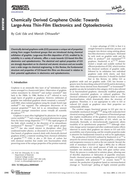
Figure 1. Process scheme for fabricating rGO-based thin films. The<br />
schematic illustrations show the structure of the material at each stage<br />
of the process. The gray <strong>and</strong> the orange sheets represent not oxidized<br />
<strong>and</strong> oxidized graphene sheets, repectively.<br />
Graphite oxide in water hydrolyzes to form thin platelets,<br />
which are negatively charged. While Brodie [84] remarked that<br />
the platelets were ‘‘extremely thin,’’ it was about 100 years<br />
later when Boehm et al. [1] concluded that the thinnest<br />
graphite oxide platelets consisted of single-carbon-thick layers.<br />
Today, the existence of monolayers of graphite oxide is widely<br />
acknowledged <strong>and</strong> recognized as graphene oxide (GO). [32,34] The<br />
term ‘‘platelets’’ is often used to describe thick multilayers of GO<br />
or rGO, while ‘‘sheets’’ usually indicate a monolayer to few<br />
layers. [93]<br />
Individual sheets of GO can be viewed as graphene decorated<br />
with oxygen functional groups on both sides of the plane <strong>and</strong><br />
around the edges as described by Lerf et al. [94,95] (Fig. 2a). Due to<br />
ionization of carboxyl groups, which are primarily present at the<br />
sheet edges (Fig. 2a), GO can be electrostatically stabilized to form<br />
a colloidal suspension [96] in water, alcohols, <strong>and</strong> certain organic<br />
solvents [97,98] without surfactants. Exfoliation of graphite oxide<br />
into individual sheets can be facilitated by ultrasonic agitation [33]<br />
or rapid heating [99,100] but excessive ultrasonication can result in<br />
decrease of lateral dimensions. [72,101]<br />
Oxidation of graphite results in a brown-colored viscous<br />
slurry, which contains graphite oxide <strong>and</strong> exfoliated sheets<br />
along with nonoxidized graphitic particles <strong>and</strong> residue of the<br />
oxidizing agents. After repeated centrifugation, sedimentation,<br />
or dialysis, salts <strong>and</strong> ions from the oxidation process can be<br />
removed from GO suspensions (see for example, Ref.<br />
[42,89,96,102]). To achieve a suspension of monolayer GO,<br />
nonoxidized graphitic particles <strong>and</strong> thick graphite oxide<br />
platelets are precipitated out by further centrifugation.<br />
Suspensions of GO flakes that are monodispersed according<br />
to their lateral size can also be obtained by density-gradient<br />
centrifugation. [101]<br />
The thickness of a monolayer GO sheet is approximately<br />
1–1.4 nm, which is thicker than an ideal monolayer of graphene<br />
(thickness 0.34 nm) due to the presence of functional groups<br />
<strong>and</strong> adsorbed molecules (Fig. 3a). [32,103] Since the functional<br />
groups make GO strongly hydrophilic, multilayered GO contains<br />
trapped water molecules between the layers. [94,103,104] Studies<br />
have shown that these molecules can be partially removed from<br />
the structure during thermal reduction [103,105] (Fig. 3b). Despite<br />
the difference in their optical properties, like pristine graphene,<br />
[106,107] GO sheets are also readily visible on Si substrates<br />
with 300-nm SiO 2 (Fig. 3c). [108] Furthermore, high-contrast<br />
visualization of GO on arbitrary substatrates can be achieved by<br />
fluorescence quenching microscopy. [109,110] The maximum lateral<br />
size of GO sheets is dependent on the size of initial graphite<br />
crystals, but the average size can be adjusted to some degree by<br />
the extent of oxidation procedure [111] or by ultrasonication. [72,101]<br />
Large <strong>and</strong> small GO sheets observed with optical <strong>and</strong> atomic force<br />
microscopy (AFM), shown in Figure 3c–e, respectively, demonstrate<br />
the wide range of lateral sizes. By using large graphite<br />
crystals as the starting material <strong>and</strong> employing a multistep<br />
oxidation process, GO sheets as large as 3 mm have been<br />
synthesized. [112] Due to the ease of identification on SiO 2 /Si<br />
substrates <strong>and</strong> their large lateral size, GO sheets can be contacted<br />
with metal electrodes for electrical studies using st<strong>and</strong>ard<br />
lithographic techniques. [113] On the other h<strong>and</strong>, GO sheets<br />
having lateral sizes of few nanometers have also been observed<br />
after extensive ultrasonication. [101]<br />
2.2. Reduction of <strong>Graphene</strong> <strong>Oxide</strong><br />
There are a number of routes for reduction of GO, as briefly<br />
summarized in recent reviews. [26,30] Chemical methods involve<br />
exposure of GO to reducing chemicals such as hydrazine<br />
(hydrazine monohydrate, [32,113,114] dimethylhydrazine, [34,42] <strong>and</strong><br />
anhydrous hydrazine [115] ), hydrides (sodium borohydride [116–119]<br />
<strong>and</strong> sodium hydride [120] ), hydroquinone, [116,121] <strong>and</strong> p-phynylene<br />
diamine. [122] Reduction of GO also occurs in strongly alkaline<br />
environments [123] <strong>and</strong> in supercritical water. [124] Thermal reduction<br />
of GO is typically achieved above 200 8C in inert or reducing<br />
environments <strong>and</strong> becomes more efficient at higher temperatures.<br />
[60,61,125] It should be noted that in the presence of oxygen,<br />
GO decomposes quickly at high temperatures [32] <strong>and</strong> gradually at<br />
lower temperatures (
www.MaterialsViews.com<br />
www.advmat.de<br />
electronic structures of GO <strong>and</strong> rGO are<br />
discussed in Section 3 <strong>and</strong> their ramification<br />
on the optoelectronic properties are described in<br />
Section 4.<br />
REVIEW<br />
Figure 2. a) Chemical structure model of GO. Position of oxygen functional groups are<br />
indicated by circles. The functional groups are attached on both sides of the graphene sheet.<br />
Reproduced with permission from [94]. Copyright 1998, American Chemical Society. b) 3D view<br />
of a GO sheet. In reality, the sheets are corrugated due to puckering caused by the functional<br />
groups. Reproduced with permission from [96]. Copyright 2009, American Chemical<br />
Society.<br />
Multistep reduction based on a combination of different<br />
processes is also an effective route for removing specific<br />
functional groups. [83] The present reduction methods utilizing<br />
hydrazine <strong>and</strong> high-temperature annealing are not ideal for<br />
environmental <strong>and</strong> technological reasons, respectively.<br />
Efficiency of the reduction process depends largely on the<br />
methods <strong>and</strong> various parameters used. [43] However, none of the<br />
reported reduction methods yield complete removal of oxygen,<br />
resulting in only partial restoration of sp 2 conjugated graphene<br />
network. In addition, thermal reduction processes lead to the<br />
creation of vacancies in the basal plane due to the evolution of<br />
carbon in the form of CO or CO 2 . [99,132] Although it has been<br />
argued that hydrazine reduction proceeds without evolution of<br />
carbon, [32] experimental evidence for this is been available. The<br />
structure of chemically <strong>and</strong>/or thermally reduced GO has not<br />
been widely investigated theoretically [133,134] <strong>and</strong>, therefore,<br />
information regarding residual oxygen groups in rGO is limited.<br />
However, it is known that residual C O sites <strong>and</strong> vacancies<br />
introduce substantial disorder in rGO, which hinders charge<br />
transport through the atomically thin plane. The atomic <strong>and</strong><br />
2.3. Thin-Film Deposition<br />
GO sheets can be deposited on virtually<br />
any substrate in the form of thin films using<br />
techniques such as drop-casting, [99,113] dipcoating,<br />
[60] spraying, [135] spin-coating, [40,41,61,73,136]<br />
electrophoresis, [122,127] Langmuir–Blodgett<br />
(L–B) [96,137] /Langmuir–Schaefer [138] <strong>and</strong> transfer<br />
via vacuum filtration. [42,43,62] Control over<br />
film uniformity, surface morphology, thickness,<br />
<strong>and</strong> surface coverage depend on the deposition<br />
methods <strong>and</strong> parameters used. Drop-casting,<br />
dip-coating, <strong>and</strong> spraying often result in nonuniform<br />
deposition due to aggregation of GO,<br />
allowing poor control over the film thickness.<br />
Once deposited, the van der Waals forces are<br />
sufficient to keep the GO sheets strongly<br />
adhered to the substrate. [42] Individual sheets<br />
are held together with strong hydrogen bonding,<br />
which also helps the films adhere to hydrophilic<br />
surfaces. [40] To encourage adhesion on glass<br />
substrates, their surfaces can be treated<br />
with acid [96,136] or (aminopropyl)triethoxysilane<br />
(APTES) prior to deposition. [61]<br />
For spin-coating, GO suspensions with<br />
relatively high concentrations (0.5–3 mg mL 1 )<br />
are required to yield uniform continuous<br />
films. [40,41,61,73] Rapid evaporation of solvent<br />
during spin-coating is critical to allow greater<br />
interaction between the GO sheets <strong>and</strong> the<br />
substrate surface, thereby increasing the adhesion<br />
(Fig. 4a). Spin-coating typically results in<br />
the deposition of films with minimal wrinkling.<br />
Film thicknesses can be controlled by adjusting the GO<br />
concentration or number of spin-coating cycles (Fig. 4c).<br />
Through careful control of the solvent evaporation rate, deposition<br />
of uniform GO films on 30 cm wafers has been demonstrated. [136]<br />
Vacuum filtration has been frequently used for the fabrication<br />
of GO films [42,43,62] <strong>and</strong> free-st<strong>and</strong>ing papers. [39,139] The vacuum<br />
filtration method has also been utilized to make uniform thin<br />
films of single-walled carbon nanotubes (SWNTs) for transparent<br />
<strong>and</strong> flexible devices. [140–142] To obtain thin films of GO,<br />
suspensions with relatively low concentrations (0.5 mg L 1 )<br />
are filtered through mixed cellulose ester membranes (MCE) with<br />
nanometer-sized pores. As the suspension is passed through the<br />
ester filter, the liquid is able to pass through the pores with the aid<br />
of a vacuum pump while the GO sheets become lodged, leading to<br />
the deposition of a film on the membrane (Fig. 4b). The process<br />
allows reasonably good nanometer-scale control over the film<br />
thickness <strong>and</strong> percolation of sheets in sub-monolayer films. The<br />
GO films can then be transferred onto various substrates by<br />
gently pressing the film against substrate surface <strong>and</strong> dissolving<br />
the ester membrane [42] (Fig. 4d <strong>and</strong> e).<br />
Adv. Mater. 2010, 22, 2392–2415 ß 2010 WILEY-VCH Verlag GmbH & Co. KGaA, Weinheim 2395
www.advmat.de<br />
www.MaterialsViews.com<br />
REVIEW<br />
pronounced wrinkling, especially in the case of thick films<br />
(N 5) [143] (Fig. 5d). Patterning of GO films can be achieved<br />
using st<strong>and</strong>ard lithographic processes. Deposition of a patterned<br />
sacrificial masking layer followed by oxygen plasma etching can<br />
preferentially remove GO from unprotected regions [41,73] (Fig. 5e<br />
<strong>and</strong> f). Selected-area vaporization of GO via laser ablation allows<br />
mask-free direct patterning of films. [144]<br />
Figure 3. a) AFM image of overlapping GO sheets. The height profile<br />
shows that the thickness of individual GO sheets is approximately 1 nm.<br />
The inset shows a photograph of a GO suspension in water. Reproduced<br />
with permission from [34]. Copyright 2006, Nature Publishing Group.<br />
b) Thickness of GO sheets measured by AFM as a function of the number<br />
of layers before (open circles) <strong>and</strong> after (solid circles) thermal reduction.<br />
The inset shows schematic illustration of mono- <strong>and</strong> multilayer GO (above)<br />
<strong>and</strong> rGO (below) sheets showing an intercalating water layer in GO <strong>and</strong><br />
interfacial layer between the GO/rGO sheets <strong>and</strong> the substrate.<br />
Reproduced with permission from [103]. Copyright 2008, American<br />
Chemical Society. c) Optical microscopy image of large GO sheets<br />
deposited on a SiO 2 /Si substrate. d) AFM image of submicrometer-sized<br />
GO sheets. Reproduced with permission from [72]. Copyright 2009,<br />
American Chemical Society. e) <strong>Nano</strong>meter-sized GO sheets obtained by<br />
extensive sonication. Reproduced with permission from [101]. Copyright<br />
2008, Springer.<br />
L–B assembly has been used for controlled deposition of highly<br />
uniform GO films [96,137] (Fig. 4f). This technique exploits the<br />
electrostatic repulsive forces between the ionized edge functional<br />
groups of individual GO sheets. [102] Briefly, a suspension of GO in<br />
a mixture of water <strong>and</strong> methanol is carefully spread over the water<br />
surface to obtain floating GO sheets trapped at the water/air<br />
interface. The density of GO sheets can be controlled by varying<br />
the available water/air interface area. Since the GO sheets are<br />
electrostatically stabilized, they remain dispersed as monolayers<br />
with decreasing area until the edge-to-edge repulsive forces are<br />
overcome by the attractive forces between sheet faces, leading to<br />
stacking of layers. [96] The floating GO film is deposited onto a<br />
substrate as it is slowly raised out of the solution.<br />
GO thin films deposited on SiO 2 /Si substrates can also be<br />
transferred onto other substrates via delamination in water.<br />
Robinson et al. [40] demonstrated that treatment of GO films with<br />
sodium hydroxide solution <strong>and</strong> subsequent dipping in water<br />
leads to uniform delamination of free st<strong>and</strong>ing films floating on<br />
the water surface. The film can then be recaptured onto a desired<br />
substrate (Fig. 5g). An additional polymer support layer can be<br />
deposited to ensure that the film does not disintegrate into<br />
individual sheets during transfer. [136]<br />
Spin-coated films are generally highly continuous <strong>and</strong> cover<br />
the entire substrate (Fig. 5a), while L–B assembly is suited for<br />
producing highly uniform, close-packed monolayered GO films<br />
in the subpercolation regime (Fig. 5c). Vacuum filtration allows<br />
deposition of films with wide-ranging thicknesses but often with<br />
3. Structural Properties<br />
The determination of GO structure has been challenging because<br />
of its non-stoichiometric chemical composition, which depends<br />
on the synthesis method <strong>and</strong> the degree of reduction. Some of the<br />
key questions pertaining to the structure of GO are: i) Which<br />
functional groups are present? ii) What are the amount of <strong>and</strong><br />
iii) relative fraction of the functional groups? iv) How are they<br />
distributed spatially over the graphene plane? v) And finally, how<br />
do they evolve during reduction? Various structural models of GO<br />
have appeared in the literature over the past several decades, as<br />
summarized in Reference [145] . The recent breakthrough in<br />
the solid-state NMR characterization of 13 C-labeled graphite<br />
oxide [146] <strong>and</strong> other similar works [83,147,148] have indicated that the<br />
most probable chemical configuration is described by the<br />
[94]<br />
Lerf-Klinowski <strong>and</strong> the Dékány models [145] with minor<br />
modifications, providing satisfying answers to questions i–iii.<br />
raised above. However, the information obtained via analytical<br />
studies is not sufficient for fully underst<strong>and</strong>ing the optical <strong>and</strong><br />
electrical properties of GO/rGO, which are critically dependent<br />
on the spatial distribution of the functional groups. For example,<br />
the electron mean free path is limited by the distance between two<br />
defective sites represented either by C O or a vacancy. [149]<br />
Underst<strong>and</strong>ing the evolution of the GO structure during<br />
reduction is therefore critical. From this perspective, the<br />
following Sections review studies discussing the atomic- <strong>and</strong><br />
nanometer-scale characterization of GO.<br />
3.1. Chemical Structure<br />
The oxygen functional groups in GO have been identified by<br />
various techniques. [150] It is generally agreed that oxygen is<br />
present in GO mostly in the form of hydroxyl <strong>and</strong> epoxy groups on<br />
the basal plane, whereas smaller amounts of carboxyl, carbonyl,<br />
phenol, lactone, <strong>and</strong> quinone are present primarily at the sheet<br />
edges. Depending on the preparation method, GO with chemical<br />
compositions ranging from C 8 O 2 H 3 to C 8 O 4 H 5 , corresponding to<br />
a C:O ratio of 4:1 to 2:1 is typically produced. [150–153] After<br />
reduction, the C:O ratio can be improved to approximately 12:1 in<br />
most cases [43,99] but values as large as 246:1 have been recently<br />
reported. [83] Simulations based on density functional theory<br />
(DFT) have indicated that it becomes increasingly difficult to<br />
reduce GO with C:O ratios above 16:1. [154]<br />
Another important parameter that can be used to characterize<br />
the degree of oxidation or reduction in GO is the sp 2 carbon<br />
fraction. Since it is the p-electrons from the sp 2 carbon that largely<br />
determine the optical <strong>and</strong> electrical properties of carbon-based<br />
<strong>materials</strong>, [155] the fraction of sp 2 bonding can provide insight into<br />
the structure–property relationships. Carbon atoms bonded with<br />
2396 ß 2010 WILEY-VCH Verlag GmbH & Co. KGaA, Weinheim Adv. Mater. 2010, 22, 2392–2415
www.MaterialsViews.com<br />
www.advmat.de<br />
Figure 4. a) Schematic illustration of spin-coating deposition of GO thin films. The N 2 jet is used to<br />
facilitate solvent evaporation during deposition. Reproduced with permission from [40]. Copyright 2008,<br />
American Chemical Society. b) Schematic illustration of the filtration of a GO suspension. The photograph<br />
shows the GO film captured on the filtration membrane. Reproduced from with permission [42]. Copyright<br />
2008, Nature Publishing Group. c) Photograph of the as-deposited GO film (leftmost) <strong>and</strong> a series of<br />
thermally reduced GO films with increasing thickness on quartz substrates. The scale bar is 1 cm.<br />
Reproduced with permission from [61]. Copyright 2008, American Chemical Society. d) Photograph of a<br />
large-area rGO film (10 cm in diameter) on glass obtained via a vacuum-filtration method. Reproduced<br />
with permission from [42]. Copyright 2008, Nature Publishing Group. e) Photograph of a vacuum-filtered<br />
10-mm-thick rGO film exhibiting a shiny metallic luster. Reproduced with permission from [102]. Copyright<br />
2008, Nature Publishing Group. f) Photograph of a L–B CDG film. The scale bar is 10 mm. Reproduced<br />
with permission from [137]. Copyright 2008, Nature Publishing Group. g) Photograph of a rGO film<br />
released onto water surface. The film has the same dimension as the parent substrate seen on the bottom<br />
of the petri dish. Reproduced with permission from [40]. Copyright 2008, American Chemical Society.<br />
hydroxyl <strong>and</strong> epoxy groups are sp 3 hybridized <strong>and</strong> thus are<br />
dominant in as-synthesized GO. It should be noted that the C:O<br />
ratio does not directly translate into an sp 2 fraction, because<br />
one hydroxyl group is attached to one sp 3 carbon, whereas<br />
one epoxy group is attached to two sp 3 carbon atoms.<br />
Further, the relative fraction of these groups may vary with<br />
different methods of oxidation. [26] Mattevi et al. [43] have recently<br />
shown with XPS analysis that the sp 2 -bonded carbon fraction<br />
increases from 40% in pristine GO to 80% in thermally<br />
reduced GO.<br />
3.2. Atomic Structure<br />
An ideal sheet of graphene consists of only trigonally bonded sp 2<br />
carbon atoms <strong>and</strong> is perfectly flat, [156] apart from the microscopic<br />
ripples. [157] On the other h<strong>and</strong>, a GO sheet consists partly of<br />
tetrahedrally bonded sp 3 carbon atoms, which are displaced<br />
slightly above or below the graphene plane. [99] Due to the<br />
structural deformation <strong>and</strong> covalently bonded functional groups,<br />
GO sheets are atomically rough. [98] Despite the presence of<br />
atomic-scale protrusions, the GO<br />
sheets can efficiently stack on one<br />
another [158] leading to graphite-like<br />
layered structure, or graphite oxide<br />
(Fig. 6a). The interlayer spacing<br />
depends on the relative humidity due<br />
to the hygroscopic nature of GO <strong>and</strong><br />
ranges from 0.6 to 1.2 nm for dry<br />
<strong>and</strong> hydrated samples. [104] During<br />
thermal reduction, the trapped water<br />
molecules diffuse out of the structure<br />
<strong>and</strong> the functional groups evolve as<br />
gases, thereby leading to slight shrinking<br />
of the interlayer spacing. [103,105]<br />
Removal of carbon from the GO<br />
backbone generates defects such as<br />
double vacancies, often referred to as<br />
5–8–5 defects, <strong>and</strong> Stone–Wales or<br />
5–7–7–5 defects. [99,159]<br />
Carbon <strong>materials</strong> consisting of both<br />
sp 2 -<strong>and</strong> sp 3 -hybridized atoms are<br />
typically amorphous, possessing poor<br />
or no translational symmetry. [155]<br />
Surprisingly, reports show that the<br />
graphene-like honeycomb lattice in<br />
GO is preserved, albeit with disorder,<br />
consistent with the early studies on<br />
graphite oxide indicating its crytalline<br />
nature. [160,161] That is, the carbon<br />
atoms attached to functional groups<br />
are slightly displaced but the overall<br />
size of the unit cell in GO remains<br />
similar to that of graphene. GO is<br />
therefore structurally similar to partially<br />
hydrogenated graphene (or ‘‘graphane’’),<br />
which possesses the original<br />
honeycomb lattice structure despite<br />
the presence of both sp 2 <strong>and</strong> sp 3<br />
carbon. [23] The transmission electron microscopy (TEM) image<br />
of a GO monolayer (Fig. 6b) indicates its high transpancy to the<br />
electron beam in comparison to the thin amorphous carbon<br />
support. The sharp selected-area electron diffraction (SAED) spot<br />
patterns of the GO monlayer reveals that the crytalline order of<br />
the original graphene lattice is present over at least a few<br />
nanometers [162] (Fig. 6c). Wilson et al. [162] further remarked that<br />
the long-range orientational order is also present over the the<br />
entire sheet (several micrometers in size). The SAED analysis<br />
from bilayers reveal two misoriented hexagonal patterns,<br />
indicating incommensurate stacking of the GO sheets<br />
(Fig. 6d). This is not surprising as the functional groups<br />
protruding from the GO planes are expected to decouple the<br />
interactions between the carbon backbones of neighboring<br />
layers. [158,162] Evidence of AB stacking has been reported for<br />
multilayered GO, [153] however, it is possible that such samples are<br />
incompletely oxidized graphitic platelets with little or no<br />
interlayer oxygen. This must be distinguished from overlapped<br />
or stacked monolayers. High-resolution TEM (HR-TEM) has<br />
been used to image the honeycomb lattice along with disorder<br />
in GO [162] (Fig. 6e).<br />
REVIEW<br />
Adv. Mater. 2010, 22, 2392–2415 ß 2010 WILEY-VCH Verlag GmbH & Co. KGaA, Weinheim 2397
www.advmat.de<br />
www.MaterialsViews.com<br />
REVIEW<br />
the STM images reveals long-range crytalline order consistent<br />
with TEM observations. [159] P<strong>and</strong>ey et al. [164] examined the<br />
oxidized regions <strong>and</strong>, surprisingly, observed a periodic arrangement<br />
of oxygen atoms, which spanned over a few nanometers<br />
(Fig. 7b). The oxygen atoms were arranged in a rectangular lattice,<br />
suggesting a series of epoxy groups present in strips (Fig. 7c).<br />
Such arrangement of epoxy groups is energetically favorable<br />
according to DFT calculations. [165] This observation, however, is<br />
inconsistent with the SAED results, which indicate that the<br />
oxygen atoms do not form periodic structures. [162]<br />
<strong>Nano</strong>meter-scale surface corrugations of GO <strong>and</strong> rGO sheets<br />
deposited on HOPG have been recently examined using<br />
AFM. [101,163] Paredes et al. [163] showed that GO <strong>and</strong> rGO sheets<br />
exhibit globular morphology with feature sizes ranging from 5 to<br />
10 nm (Fig. 7e <strong>and</strong> 7f). The surface roughness of GO was found to<br />
be approximately 0.1 nm. It is tempting to attribute this<br />
roughness to the C O groups protruding from the carbon<br />
backbone, as the C O bond length [166] coincides with this length<br />
scale. Although some similarities can be found between the<br />
topographic image shown in Figure 7e <strong>and</strong> the oxygen<br />
distribution map from the ADF image (Fig. 6f), the length scale<br />
of the fluctuations differs appreciably, suggesting that the<br />
observed undulations of GO <strong>and</strong> rGO are associated with carbon<br />
backbone distortions rather than the functional groups.<br />
3.3. Raman Spectroscopy<br />
Figure 5. a) AFM image of 20 nm-thick spin-coated GO film on silicon<br />
substrate. Reproduced from [73]. Copyright 2009, Wiley-VCH. b) Optical<br />
microscopy image of a percolating network of rGO sheets on a SiO 2 /Si<br />
substrate prepared by vacuum filtration. The corresponding SEM image<br />
shown in the inset shows the contrast between the conductive rGO <strong>and</strong> the<br />
insulating substrate. Reproduced with permission from [42]. Copyright<br />
2008, Nature Publishing Group. c) SEM image of a subpercolating GO<br />
network deposited via L–B method. Reproduced with permission from [96].<br />
Copyright 2009, American Chemical Society. d) AFM image of GO film<br />
exhibiting extensive surface wrinkles prepared by a vacuum filtration<br />
method. [143] e) Optical microscopy image showing a patterned rGO film<br />
with interdigitated Ti/Au electrodes used for molecular-sensing studies.<br />
Reproduced with permission from [41]. Copyright 2008, American Chemical<br />
Society. f) Optical microscopy image of patterned rGO electrodes for<br />
organic thin-film transistors. Reproduced from [73].<br />
Oxygen functional groups of GO are uniformly but r<strong>and</strong>omly<br />
attached on the graphene plane. Mkhoyan et al. [158] recently<br />
examined the oxygen distribution on a GO monolayer using<br />
high-resolution annular dark field (ADF) imaging in a scanning<br />
transmission electron microscopy (STEM) instrument, as shown<br />
in Figure 6f. The results indicate that the degree of oxidation<br />
fluctuates at the nanometer-scale, suggesting the presence of<br />
sp 2 <strong>and</strong> sp 3 carbon clusters of a few nanometers. Several<br />
groups [113,159,163] have studied the surface of GO with scanning<br />
tunneling microscopy (STM) <strong>and</strong> observed highly defective<br />
regions, probably due to the presence of oxygen <strong>and</strong> other areas<br />
that were nearly intact (Fig. 7a <strong>and</strong> b). Fourier transformation of<br />
Raman spectroscopy is a non-destructive technique that is widely<br />
used to obtain structural information about carbon-based<br />
<strong>materials</strong>. [167] The main features in the Raman spectra of<br />
graphitic carbon-based <strong>materials</strong> are the G <strong>and</strong> D peaks <strong>and</strong> their<br />
overtones. The first-order G <strong>and</strong> D peaks, both arising from<br />
vibrations of sp 2 carbon, appear at around 1580 <strong>and</strong> 1350 cm 1 ,<br />
respectively. The G peak corresponds to optical E 2g phonons at the<br />
Brillouin zone center <strong>and</strong> is due to bond stretching of sp 2 carbon<br />
pairs in both rings <strong>and</strong> chains. The D peak is due to the breathing<br />
mode of aromatic rings <strong>and</strong> requires a defect for its activation. [168]<br />
The D-peak intensity is therefore often used as a measure for the<br />
degree of disorder. [167] The overtone of the D peak, called 2D peak,<br />
appears around 2680 cm 1 , <strong>and</strong> its shift <strong>and</strong> shape has been<br />
correlated with the number of graphene layers (N). [169–171] The 2D<br />
peak is attributed to double resonance transitions resulting in<br />
production of two phonons with opposite momentum.<br />
Furthermore, unlike the D peak, which is only Raman active<br />
in the presence of defects, the 2D peak is active even in the<br />
absence of any defects.<br />
Typical Raman spectra of monolayers of GO <strong>and</strong> rGO obtained<br />
at an excitation wavelength of 532 nm are shown in Figure 8. The<br />
general features of the spectra for GO are similar to those seen in<br />
partially hydrogenated graphene [23] but deviate from those of<br />
mechanically exfoliated graphene, where the D peak is absent <strong>and</strong><br />
the peaks are more clearly defined. [172] The prominent D peak<br />
(1350 cm 1 ) with intensity comparable to the G peak<br />
(1600 cm 1 ) along with their large b<strong>and</strong> width are indicative<br />
of significant structural disorder in GO. Weak <strong>and</strong> broad 2D<br />
peaks are another indication of disorder. [173] It should be noted<br />
that for mechanically exfoliated graphene, the 2D peak is sharp<br />
with FWHM of 30 cm 1 (as opposed to 200 cm 1 for GO) <strong>and</strong><br />
2398 ß 2010 WILEY-VCH Verlag GmbH & Co. KGaA, Weinheim Adv. Mater. 2010, 22, 2392–2415
www.MaterialsViews.com<br />
www.advmat.de<br />
Figure 6. a) TEM image <strong>and</strong> corresponding SAED pattern (inset) of a thick rGO film. Reproduced<br />
with permission from [60]. Copyright 2007, American Chemical Society. b) TEM image of a<br />
monolayer GO flake. SAED pattern of c) a monolayer <strong>and</strong> d) a bilayer region of a GO flake.<br />
e) High-resolution TEM image of a monolayer GO. The inset shows the Fourier transform of the<br />
image. Reproduced with permission from [162]. Copyright 2009, American Chemical Society.<br />
f) ADF image of a GO monolayer showing contrast between oxygen-free <strong>and</strong> oxidized regions.<br />
Reproduced with permission from [158]. Copyright 2009, American Chemical Society.<br />
exhibits higher intensity than the G peak. [172] A<br />
defect-activated peak called D þ D’ is also<br />
readily visible near 2950 cm 1 (Ref. [23]).<br />
The overall Raman peak intensities are<br />
diminished after reduction treatment, suggesting<br />
loss of carbon during reduction (not<br />
illustrated in Fig. 8). [143,174]<br />
The G peak of GO <strong>and</strong> rGO is shifted to<br />
higher frequencies with respect to that of<br />
graphene <strong>and</strong> graphite. This G-peak stiffening<br />
is often associated with doping effects. [175]<br />
Indeed, a doping-induced G-peak shift in<br />
as-synthesized GO has been identified in ionic<br />
screening [176] <strong>and</strong> charge-transfer [177] studies.<br />
However, the fact that G-peak stiffening is<br />
commonly observed in GO <strong>and</strong> defective<br />
graphene [149] but not in mechanically exfoliated<br />
graphene under similar conditions<br />
suggests that other effects related to disorder<br />
may play a more significant role. A possible<br />
interpretation of the G-peak stiffening is based<br />
on the presence of isolated short double-bond<br />
segments. [167] Kudin et al. [159] simulated the<br />
Raman spectra of GO with various oxygen<br />
distributions <strong>and</strong> found that the blue shift of<br />
the G peak is possible if alternating single–<br />
double bond segments are present within<br />
REVIEW<br />
Figure 7. a) STM image of a GO monolayer on a HOPG substrate. Regions enclosed by green contours are populated with oxygen functional groups.<br />
Reproduced with permission from [113]. Copyright 2007, American Chemical Society. b) STM image of a rGO monolayer on a HOPG substrate <strong>and</strong> its<br />
Fourier transform (upper-right inset). The lower-left inset shows a STM image of a HOPG surface obtained under identical conditions. Reproduced with<br />
permission from [159]. Copyright 2008 American Chemical Society. c) High-resolution STM image of the oxidized region of GO revealing a rectangular<br />
lattice. The size of the lattice vectors a <strong>and</strong> b correspond to 0.273 <strong>and</strong> 0.406 nm, respectively. d) Schematic image of the rectangular lattice formed by a<br />
series of epoxy groups. Reproduced with permission from [164]. Copyright 2008, Elsevier. Tapping mode AFM e) height image <strong>and</strong> corresponding height<br />
profile (f) of GO on HOPG. Reproduced with permission from [163]. Copyright 2009, American Chemical Society.<br />
Adv. Mater. 2010, 22, 2392–2415 ß 2010 WILEY-VCH Verlag GmbH & Co. KGaA, Weinheim 2399
www.advmat.de<br />
www.MaterialsViews.com<br />
REVIEW<br />
Figure 8. Raman spectra of a monolayer of GO, rGO, <strong>and</strong> mechanically<br />
exfoliated graphene on SiO 2 /Si substrates normalized to the G-peak<br />
intensity. Reproduced with permission from [186]. Copyright 2008, American<br />
Chemical Society.<br />
nanoribbon-shaped clusters of sp 2 carbon. However, such specific<br />
structures in GO do not agree with TEM observations. The origin<br />
of the G peak blue shift therefore requires additional clarification.<br />
The 2D peak intensity in GO <strong>and</strong> rGO is typically weak <strong>and</strong><br />
careful data acquisition is necessary to study its characteristics. [42]<br />
Nevertheless, the position of the 2D peak for GO <strong>and</strong> rGO is<br />
consistent with that of the monolayer of mechanically exfoliated<br />
graphene. [169] In commensurately stacked multilayers of graphene,<br />
the 2D peak splits into two major <strong>and</strong> two minor<br />
components due to coupling between the layers. [169,171] Their<br />
positions slightly blue-shift with increasing N up to N 5 when<br />
the features are difficult to distinguish from those of graphite.<br />
The 2D-peak splitting in rGO spectra has been reported [42] but is<br />
often absent, probably due to weak interlayer coupling. [178] In<br />
multilayered GO, the 2D peak has been found to blue-shift with<br />
reduction, suggesting stronger interlayer coupling accompanied<br />
by removal of trapped interlayer species <strong>and</strong> functional<br />
groups. [179]<br />
During thermal reduction, GO undergoes structural changes<br />
due to evolution <strong>and</strong> rearrangement of oxygen <strong>and</strong> carbon atoms.<br />
Such structural changes have been investigated by in situ <strong>and</strong><br />
ex situ Raman spectroscopy for GO subjected to thermal<br />
annealing at various temperatures. [43,179] It is well documented<br />
[168,180–182] that the area ratio of the D <strong>and</strong> G peaks is a measure<br />
of the size of sp 2 ring clusters in a network of sp 2 <strong>and</strong> sp 3 carbon.<br />
Using the empirical Tuinstra–Koenig relation, [168] the average<br />
graphitic domain size in as-synthesized GO has been calculated<br />
<strong>and</strong> values ranging from 2.5 to 6 nm have been reported. [43,113]<br />
These values are in reasonable agreement with the size of the<br />
spatial fluctuations in oxygen (Fig. 6d), as discussed above.<br />
Variable effects of reduction on the sp 2 domain size in GO<br />
have been reported in the literature. The D/G ratio has been<br />
reported to increase, [32,115,163] decrease, [120,127,183] remain nearly<br />
constant, [43,113] or decrease following an increase. [83,184] In all<br />
cases, appreciable D-peak signal has been observed, indicating<br />
that significant disorder remains in the reduced sample. Mattevi<br />
et al. [43] reported that the D/G ratio remains nearly constant<br />
before <strong>and</strong> after thermal reduction <strong>and</strong> is independent of the<br />
annealing temperature. This observation suggests that even when<br />
the sp 2 sites are restored by de-oxidation, reduction does not lead<br />
to an expansion of the original sp 2 clusters. This is only possible if<br />
the sp 2 sites generated by reduction are isolated from the<br />
originally present sp 2 clusters by defects such as vacancies or<br />
residual sp 3 carbon. Underst<strong>and</strong>ing the discrepencies in the<br />
reported results requires further consideration into the reduction<br />
mechanism as well as optical cross-section of sp 2 clusters of<br />
various configurations.<br />
It should also be noted that the applicability of the<br />
Tuinstra–Koenig relation should be carefully checked as it is<br />
not valid above a critical defect density. In highly disordered<br />
amorphous <strong>materials</strong>, where the sp 2 cluster size is smaller than<br />
2 nm, the D/G ratio increases with the number of aromatic<br />
rings, opposite to what is expected from the Tuinstra–Koenig<br />
relation. It has been shown recently [112] that the 2D/G ratio can be<br />
also used as the measure of order. This parameter has been found<br />
to correlate better with the carrier mobility. [112]<br />
4. Electronic <strong>and</strong> Optoelectronic Properties<br />
The properties of GO <strong>and</strong> rGO thin films can be tuned by varying<br />
the coverage of sheets, film thickness, chemical composition,<br />
average flake size, <strong>and</strong> film morphology. Unlike SWNTs, which<br />
are inhomogenous due to diameter- <strong>and</strong> chirality-dependent<br />
electronic properties, individual sheets of GO <strong>and</strong> rGO exhibit<br />
nearly identical properties. [113,185,186] Instead, the properties of<br />
GO <strong>and</strong> rGO depend heavily on their chemical <strong>and</strong> atomic<br />
structures. By appropriately tuning the deposition <strong>and</strong> reduction<br />
parameters, the films can be made insulating, semiconducting, or<br />
semimetallic, while maintaining optical transparency. Further,<br />
incorporation of rGO sheets into composites allows exploitation<br />
of rGO-host interactions, offering additional degrees of freedom<br />
in device functions.<br />
It is well established that an ideal sheet of graphene is a<br />
zero-gap semiconductor. [9] The valence <strong>and</strong> the conduction b<strong>and</strong>s<br />
of graphene meet at the Fermi energy, where the density of states<br />
(DOS) of the two b<strong>and</strong>s vanishes linearly. [187] In multilayered<br />
graphene, overlap of the two b<strong>and</strong>s gives rise to finite DOS at the<br />
Fermi level, rendering it semimetallic. [188] In contrast to the large<br />
body of work devoted to underst<strong>and</strong>ing the electronic structure of<br />
graphene <strong>and</strong> graphite, [189] little attention has been devoted to<br />
equivalent information on GO <strong>and</strong> rGO <strong>and</strong> their multilayers due<br />
to complications arising from structural disorder. The fundamental<br />
properties of GO <strong>and</strong> rGO such as the energy b<strong>and</strong>gap<br />
have not yet been well understood until recently. In the following<br />
Sections, experimental results providing insight into the<br />
electronic structure <strong>and</strong> transport properties of GO <strong>and</strong> rGO<br />
are highlighted, while discussing their manifestation in device<br />
properties.<br />
4.1. Optical Properties<br />
A suspension of GO in water is dark brown to light yellow,<br />
depending on the concentration, whereas that of rGO appears<br />
black, indicating appreciable differences in the electronic<br />
2400 ß 2010 WILEY-VCH Verlag GmbH & Co. KGaA, Weinheim Adv. Mater. 2010, 22, 2392–2415
www.MaterialsViews.com<br />
www.advmat.de<br />
structure. Similar changes in the physical appearance are also<br />
observed in thin films. When rGO films are sufficiently thin<br />
(
www.advmat.de<br />
www.MaterialsViews.com<br />
REVIEW<br />
4.2. Electrical Conductivity<br />
As-synthesized GO films are typically insulating, exhibiting sheet<br />
resistance (R s ) values of about 10 12 V sq 1 or higher. [61] An<br />
exception is when GO is synthesized by carefully minimizing the<br />
oxidation level such that as-synthesized GO film is semiconducting.<br />
[201] The insulating nature of GO is attributed to the absence<br />
of percolating pathways among sp 2 carbon clusters to allow<br />
classical carrier transport to occur. Reduction of GO results in<br />
decrease in R s by several orders of magnitude. [186] Measurements<br />
on an individual sheet of rGO show that even in well-reduced<br />
samples (annealed at 1000 8C in H 2 ), the sheet resistance is<br />
0.34 MV sq 1 , [183] which is two orders of magnitude higher than<br />
that of ideal dopant-free graphene. [7] This is attributed to disorder<br />
arising from residual oxygen functional groups <strong>and</strong> presence of<br />
defects generated by evolved carbon. López et al. [185] recently<br />
demonstrated that vacancies can be ‘‘repaired’’ partialy by<br />
exposing rGO to a carbon source such as ethylene at elevated<br />
temperatures (800 8C), similar to conditions used for CVD growth<br />
of SWNTs. With this post-reduction deposition of carbon, the<br />
sheet resistance of individual rGO sheet can be decreased to<br />
28.6 kV sq 1 with a corresponding conductivity of 350 S<br />
cm 1 . [138,185] Su et al. [65] reported a similar defect healing effect<br />
for rGO sheets functionalized with aromatic molecules. In their<br />
composite system, thermal fusion of the molecules with rGO<br />
during pyrolysis resulted in a highly graphitic material with<br />
conductivity as high as 1314 S cm 1 . [65] In films, despite the<br />
presence of sheet-to-sheet junctions, R s can fall well below that of<br />
individual monolayer since the rGO layers are equivalent to<br />
‘‘parallel resistors’’. [113] Indeed, R s can be varied over several<br />
orders of magnitude depending on the degree of percolation <strong>and</strong><br />
film thickness. [42,61]<br />
The changes in the electrical conductivity (s ¼ (R s t) 1 where t<br />
is the film thickness) as well as optical transmittance of rGO films<br />
using chemical <strong>and</strong> thermal reduction treatments are shown in<br />
Figure 10. Upon exposure to hydrazine monohydrate vapor, the<br />
film conductivity immediately increases <strong>and</strong> reaches a saturation<br />
value (10 S cm 1 ; Fig. 10a). It should be noted that for thick<br />
films (N 5), reduction by hydrazine vapor is effective only for<br />
the top few layers of the GO films, resulting in a saturation of R s<br />
with increasing film thickness. [42] Additional improvement in<br />
conductivity can be achieved by annealing the hydrazine-reduced<br />
GO films in Ar/H 2 ambient (Fig. 10b). When GO films are<br />
reduced by directly annealing in Ar/H 2 without prior exposure to<br />
hydrazine, a relatively high annealing temperature (>500 8C) is<br />
required to achieve conductivity comparable to those of films<br />
reduced at low temperature by hydrazine. In both cases, the<br />
highest conductivity (550 S cm 1 ) is achieved at an annealing<br />
temperature of 1100 8C. The trends in the conductivity are<br />
consistent with the chemical composition evolution, which<br />
indicates that high C:O ratios are achieved only at high annealing<br />
temperatures. It should be noted that the presence of H 2 in the<br />
annealing environment does not have a significant impact on the<br />
achieved conductivity (Fig. 10b) <strong>and</strong> C:O ratios. [179] The<br />
conductivity values reported for pyrolyzed few-layer GO films<br />
are consistently on the order of 500 S cm 1 , irrespective of the<br />
oxidation or deposition methods used. [43,60,61,73] This value is<br />
comparable to that of polycrystalline graphite (10 3 Scm 1 ) [202]<br />
but is more than an order of magnitude lower than the in-plane<br />
Figure 10. Electrical <strong>and</strong> optical properties of 3 layer GO film. a) Conductivity<br />
<strong>and</strong> c) transmittance at l ¼ 550 nm of GO film as a function of<br />
exposure time to hydrazine monohydrate vapor at 80 8C. b) Conductivity<br />
<strong>and</strong> d) transmittance at l ¼ 550 nm of GO reduced with hydrazine monohydrate<br />
vapor for 24 h at 80 8C after annealing at different temperatures in<br />
Ar/H 2 (solid circle) <strong>and</strong> that of pristine GO after annealing in Ar/H 2 (open<br />
circle) <strong>and</strong> in UHV (triangles). Reproduced from [43].<br />
conductivity of HOPG (10 4 Scm 1 ). [203] It is also worth noting<br />
that similar conductivity has been achieved in graphene-like films<br />
obtained by pyrolysis of thin photoresist layers. [204]<br />
4.3. Transparent <strong>and</strong> Conducting Properties<br />
Transparent <strong>and</strong> conducting electrodes for optoelectronic devices<br />
is one of the most anticipated applications of graphene given its<br />
extraordinary conductivity <strong>and</strong> atomic thickness. [25] An ideal<br />
sheet of graphene exhibits R s of 6kV sq 1 with nearly constant<br />
optical transparency of 98% in the visible-IR range. [24] While<br />
6kV sq 1 is too large for typical opto-electronic devices, R s as low<br />
as a few hundred V sq 1 , which is satisfactory for many<br />
transparent conductor applications, can be reached by doping. [22]<br />
These values compare well with commercially used metal oxide<br />
films such as indium tin oxide (ITO) which exhibit R s of
www.MaterialsViews.com<br />
www.advmat.de<br />
Figure 11. Transmittance at l ¼ 550 nm as a function of sheet resistance<br />
of rGO films reported by various groups in the literature. In some cases,<br />
indicated by (*), the properties were estimated from the information<br />
provided. The stars represent the values for the same film thickness<br />
annealed at different temperatures. The asterisk in the plot corresponds<br />
to the values for ideal grapheme, whose transmittance <strong>and</strong> sheet resistance<br />
are 98% [24] <strong>and</strong> 6.45 kV, [7] respectively.<br />
that thin films of rGO can be made transparent <strong>and</strong> conducting by<br />
optimizing the thickness <strong>and</strong> reducing at high temperatures.<br />
Researchers have employed various oxidation, exfoliation,<br />
dispersion, deposition, <strong>and</strong> reduction procedures, <strong>and</strong> thus a<br />
range of transmittance <strong>and</strong> sheet resistance values have been<br />
reported in the literature, as summarized in Figure 11. The plot<br />
shows that the transmittance <strong>and</strong> sheet resistance decrease with<br />
reduction <strong>and</strong> the overall film thickness. Similar trends indicated<br />
by the bold arrows (Fig. 11) are observed in all reports. Efficient<br />
reduction is the key to achieving highly conductive films, while<br />
the ability to controllably deposit films with nanometer thickness<br />
allows high optical transparencies. Currently, the highest degree<br />
of reduction is achieved via pyrolysis at 1100 8C, yielding films<br />
with the best properties. R s as low as few kV sq 1 has been<br />
achieved with transmittance of 90% with high temperature<br />
pyrolysis. Such sheet resistance values are approximately one<br />
order of magnitude higher than those achieved with SWNT<br />
network thin films at similar transmittance values. [207]<br />
In order for rGO films to be competitive with other<br />
solution-processed alternatives to ITO such as SWNT [207] <strong>and</strong><br />
metal nanowire [208] thin films that can be deposited at room<br />
temperature <strong>and</strong> used on plastic platforms, high-temperature<br />
reduction must be avoided. Direct exfoliation <strong>and</strong> reduction of<br />
GO in hydrazine is a room-temperature route for producing<br />
highly reduced GO but yields films with moderate optoelectronic<br />
properties [209] (Fig. 11). In addition, use of highly toxic hydrazine<br />
requires extreme caution. Efforts in achieving efficient reduction<br />
of GO via less hazardous routes at room temperature <strong>and</strong> doping<br />
have provided promising prospects. [62,83,118,123,128] It should be<br />
noted that, rather surprisingly, graphene thin films produced via<br />
direct exfoliation of graphite in organic solvents [54,55,57] yield<br />
values that are comparable to or worse than those of well-reduced<br />
GO. The small size of graphene flakes obtained via this route is<br />
most likely responsible for the moderate conductivity.<br />
To translate the transparent <strong>and</strong> conducting properties into<br />
optoelectronic devices, several groups have demonstrated the use<br />
of rGO thin films as window electrodes for photovoltaic<br />
[60,62,63,65,66] <strong>and</strong> light-emitting [210] devices. Efficient collection<br />
of carriers in solar cells <strong>and</strong> carrier injection in light-emitting<br />
diodes (LEDs) depend on appropriate b<strong>and</strong> alignment of each<br />
component of the device <strong>and</strong> the electrical resistance of carrier<br />
transport layers. Since the calculated work function of graphene<br />
(4.42 eV) [211] nearly coincides with that of ITO (4.4–4.5 eV), [212]<br />
replacement of ITO with graphene obviates the need for<br />
re-designing the commonly studied photovoltaic or LED<br />
structures. With UV photoelectron spectroscopy (UPS), the work<br />
function of rGO has been found to increase gradually from 4.2 to<br />
4.4 eV with the C:O ratio. [118] The device-structure <strong>and</strong> energyb<strong>and</strong><br />
diagrams of a dye-sensitized solar cell (DSSC) with rGO as<br />
the transparent electrode are shown in Figure 12a <strong>and</strong> 12b,<br />
respectively. [60] As the dye absorbs sun light <strong>and</strong> becomes excited,<br />
the electrons are injected into the conduction b<strong>and</strong> of TiO 2 <strong>and</strong><br />
transported to the rGO electrode. Similarly, holes are transported<br />
through the hole-transport layer (denoted as spiro-OMeTAD in<br />
Fig. 12b) <strong>and</strong> collected by the Au cathode. The I V characteristics<br />
of a rGO-based device <strong>and</strong> a control device with a fluorine tin<br />
oxide (FTO) electrode under illumination of simulated sun light<br />
are shown in Figure 12c. The comparatively lower short-circuit<br />
current (I sc ) of the rGO device is attributed to the higher sheet<br />
resistance <strong>and</strong> lower transmittance of rGO compared to those of<br />
FTO. The power conversion efficiency is therefore found to be<br />
correspondingly lower for the rGO-based device.<br />
Similar results have been reported for organic photovoltaic<br />
(OPV) devices with rGO electrodes. [62,63] In commonly studied<br />
bulk-heterojunction OPVs based on P3HT-PCBM [poly(hexyl)<br />
thiophene-[6-6]phenyl-C 61 -butyric acid methyl ester mixture]<br />
nanocomposites (Fig. 12d), holes (rather than electrons in the<br />
case of DSSC) are collected by the window electrode. [213] The<br />
rGO-based devices exhibit nearly linear I V characteristics due to<br />
the dominating series resistance of rGO <strong>and</strong> small shunt<br />
resistance giving rise to large reverse bias current (Fig. 12e). It is<br />
interesting to note that the short-circuit current <strong>and</strong> the<br />
conversion efficiency of rGO-based devices are found to be less<br />
severely influenced by the large sheet resistance of rGO films<br />
(approximately three orders of magnitude larger than that of ITO<br />
in these demonstrations) than otherwise expected from simple<br />
series resistance calculations. These findings point to the<br />
importance of investigating the rGO-organic interfacial effects. [73]<br />
4.4. Electric-Field Effect<br />
One of the well-known signatures of graphene <strong>and</strong> few-layer<br />
graphene is the electric-field-dependent transport which, along<br />
with the extraordinary carrier mobility, makes them attractive as<br />
the channel material for high-frequency field effect transistors.<br />
[214] It has been shown that thin films of rGO exhibit a<br />
graphene-like ambipoloar field effect when films are made<br />
sufficiently thin. [62] Figure 13a shows the schematic of a<br />
bottom-gated field effect device with rGO thin film as the<br />
channel material. The conductance of the channel between the<br />
source (S) <strong>and</strong> the drain (D) electrodes is modulated by a<br />
capacitively coupled gate (G) bias. It should be noted that in rGO<br />
thin-film devices, individual rGO sheets typically do not span the<br />
source <strong>and</strong> drain electrodes (Fig. 13b), thereby requiring carriers<br />
REVIEW<br />
Adv. Mater. 2010, 22, 2392–2415 ß 2010 WILEY-VCH Verlag GmbH & Co. KGaA, Weinheim 2403
www.advmat.de<br />
www.MaterialsViews.com<br />
REVIEW<br />
Figure 12. a) Schematic illustration of DSSC using rGO as the window electrode. b) The energy level diagram of DSSC consisting of rGO/TiO 2 /dye/<br />
spiro-OMeTAD/Au layers. c) I V characteristics of rGO-based (black) <strong>and</strong> FTO-based (red) DSSC under simulated solar illumination. Reproduced with<br />
permission from [60]. Copyright 2007, American Chemical Society. d) Structure of OPV having rGO film as the electrode. e) I V characteristics of<br />
rGO-based (blue) <strong>and</strong> ITO-based (red) OPV in the dark <strong>and</strong> under simulated solar illumination (data from Ref. [62] <strong>and</strong> unpublished work).<br />
to travel from one sheet to another during transport across the<br />
channel. Transfer characteristics of 1.5- <strong>and</strong> 4-layer rGO<br />
thin-film devices measured at different temperatures are shown<br />
in Figure 13c <strong>and</strong> 13d, respectively. Both devices are ambipoloar,<br />
that is, both electron <strong>and</strong> hole currents can be induced by<br />
gate bias. The ‘‘V’’ shape of the transfer characteristics is more<br />
pronounced for the low temperature measurements of the<br />
1.5-layer film <strong>and</strong> the neutrality point, at which the channel<br />
conductance reaches minimum, is clearly observed. The<br />
characteristic difference between the thin <strong>and</strong> thick films is<br />
the on/off ratio, which is defined as the ratio between the<br />
maximum to minimum conductance, G max /G min . Normalized<br />
transfer characteristics of 1.5, 2.5, <strong>and</strong> 4 layer rGO films at<br />
T ¼ 4.2 K indicates that the field effect diminishes with increasing<br />
number of layers (Fig. 13e). This observation is consistent with<br />
the fact that a monolayer of graphene is a zero-b<strong>and</strong>gap<br />
semiconductor, while a multilayer graphene is a semimetal. [188]<br />
In other words, the DOS at the neutrality point is greater for<br />
thicker films, making it difficult to turn off the devices, as is the<br />
case for mesoscopic graphite. [215] Similar effects have also been<br />
observed for mechanically exfoliated graphene devices. [216] The<br />
thickness-dependent temperature dependence of the conductivity<br />
reflects this transition. [143] The differences in the on/off ratio,<br />
however, are relatively small in mono- to few layer rGO films <strong>and</strong><br />
are less pronounced at room temperatures (Fig. 13f). The contact<br />
resistance of rGO devices is negligible compared to the channel<br />
resistance <strong>and</strong> that field effect in rGO is not a consequence of<br />
contact resistance modulation, [217] as is the case in some<br />
SWNT-based FETs. [218,219] The on/off ratio of rGO-based devices<br />
is typically low (
www.MaterialsViews.com<br />
www.advmat.de<br />
REVIEW<br />
Figure 13. a) Schematic image of rGO TFT. b) Photograph of a rGO TFT with an optical microscopy image showing the S–D region of the device. The<br />
channel (W ¼ 21 mm) consists of several rGO sheets percolating across the electrodes. c,d) Transfer characteristics of c) 1.5- <strong>and</strong> d) 4-layer films<br />
measured at different temperatures. Measurements were conducted in vacuum unless otherwise noted. Reproduced with permission from [42]. Copyright<br />
2008, Nature Publishing Group. e) Normalized channel conductance as a function of gate voltage for 1.5, 2.5, <strong>and</strong> 4 layer rGO film at T ¼ 4.2 K. The<br />
channel conductance (G(V g )) is normalized to its minimum value (G min ), which occurs at the charge neutrality point. [143] f) on/off ratio, G max /G min ,asa<br />
function of temperature for 1.5, 2.5, <strong>and</strong> 4 layer rGO films. [143]<br />
film coverage <strong>and</strong> the sp 2 carbon fraction. [221] While mobility of<br />
up to 365 cm 2 V 1 s 1 has been reported for well-reduced<br />
few-layered films, [183] typical values range between 0.001 <strong>and</strong><br />
10 cm 2 V 1 s 1 , depending largely on film thickness <strong>and</strong><br />
reduction conditions. [42] These values are several orders of<br />
magnitude lower than those of mechanically exfoliated graphene<br />
(40 000 cm 2 V 1 s 1 measured under similar conditions [222] ),<br />
indicating that residual oxygen <strong>and</strong> defects in the structure<br />
severely limit the carrier transport in rGO. Besides the intrinsic<br />
structural defects, substrate-induced charged impurities [223] <strong>and</strong><br />
contact-induced electron–hole asymmetry [224] are expected to be<br />
the limiting factors for mobility. [183] The electron mobilities are<br />
generally lower than the hole mobilities at ambient conditions,<br />
but the trend is reversed in vacuum, suggesting that adsorbed<br />
species may facilitate or limit carrier transport.<br />
Transport studies on individual sheets of rGO provide valuable<br />
information since sheet junctions effects can be<br />
excluded. [113,114,138,183,185,217,225,226] To fabricate single-rGO<br />
devices, individual sheets of GO are deposited onto substrates<br />
with prepatterned alignment marks, identified under a microscope,<br />
<strong>and</strong> contacted by metal electrodes following st<strong>and</strong>ard<br />
lithographic procedures. The transfer characteristics of an<br />
individual rGO device with different degrees of reduction are<br />
shown in Figure 14a (see figure caption for details). The<br />
ambipolar characteristics of well-reduced individual GO devices<br />
are in qualitative agreement with those of thin-film counterparts.<br />
Typical mobility values also nearly coincide with those of thin-film<br />
devices suggesting that sheet junctions in films play a minor role<br />
in carrier transport. Figure 14a clearly shows that transport<br />
properties of rGO evolve significantly with reduction treatment as<br />
GO transforms from insulator to semiconductor to graphene-like<br />
semimetal. [217] Lightly reduced GO possesses a finite energy gap<br />
<strong>and</strong> exhibits pronounced switching behavior. Consequently, these<br />
samples exhibit insulating off-states with on/off ratio exceeding<br />
10 3 at low temperatures. [217] Upon progressive reduction, rGO<br />
approaches the zero-gap limit, leading to a suppressed on/off<br />
ratio, while the field-effect mobility improves with increasing sp 2<br />
fraction.<br />
In a similar manner, the transport properties of GO can also be<br />
tailored by varying the degree of oxidation during synthesis. [201]<br />
Jin et al. [196] recently indicated that the energy gap of GO can be<br />
tuned by adjusting the oxidation time. By minimizing the<br />
oxidation time, semiconducting GO was obtained without<br />
the need for reduction. [201] There are no apparent differences<br />
in the device characteristics between those fabricated by<br />
controlled oxidation <strong>and</strong> those obtained by reduction.<br />
4.5. Electrical Conduction Mechanisms<br />
Kaiser et al. [227] reported that electrical conduction in rGO can be<br />
described by variable-range hopping (VRH) in 2D <strong>materials</strong>. In<br />
VRH, the temperature dependence of the conductivitym s is<br />
of the form [228]<br />
<br />
s ¼ s 0 exp<br />
<br />
B<br />
T 1=3<br />
(2)<br />
Adv. Mater. 2010, 22, 2392–2415 ß 2010 WILEY-VCH Verlag GmbH & Co. KGaA, Weinheim 2405
www.advmat.de<br />
www.MaterialsViews.com<br />
REVIEW<br />
Figure 14. a) Transfer characteristics of a single rGO sheet with different degrees of<br />
reduction measured at T ¼ 78 K. The labels, 8m, 15m, 30m, <strong>and</strong> 16h (m ¼ minutes,<br />
h ¼ hours) correspond to total time of exposure to hydrazine monohydrate vapor. HG-A<br />
<strong>and</strong> HG-B correspond to GO directly reduced in anhydrous hydrazine with subsequent<br />
annealing in forming gas at 150 8C. Reproduced with permission from [217]. Copyright<br />
2009, American Chemical Society. b) ln(I) as a function of T 1/3 at different gate voltages<br />
showing a fit to 2D VRH model. Reproduced with permission from [227]. Copyright 2009,<br />
American Chemical Society. c) Hopping parameter (B) <strong>and</strong> device current at 100 K (I sd )asa<br />
function of gate voltage (unpublished data from Ref. [217]).<br />
The hopping parameter B is expressed as<br />
<br />
3a 2 1=3<br />
B ¼<br />
NE ð F Þk B<br />
where a is the wavefunction decay constant, N(E F ) is the DOS at<br />
the Fermi level, <strong>and</strong> k B is the Boltzmann constant. The<br />
temperature dependence of the two-terminal current at fixed<br />
V sd <strong>and</strong> V g can be fitted well with Equation (2) as shown in<br />
Figure 14b. The slope of the linear plot corresponding to the<br />
hopping parameter –B 1/3 changes with V g , indicating that the gate<br />
bias alters the hopping condition rather than simply inducing<br />
charges. Further analysis of B 1/3 as a function of V g indicates that<br />
the hopping condition is most severe near the charge neutrality<br />
point, while hopping is facilitated at increased jV g j (Fig. 14c).<br />
These observations are also consistent with the carrier-transport<br />
mechanisms in partially hydrogenated graphene. [23]<br />
The evolution of the electronic structure during reduction is<br />
indicated by the fact the apparent activation energies associated<br />
with carrier concentration (n) <strong>and</strong> carrier mobility (m) decrease<br />
with the extent of reduction. [217] Particularly, the apparent energy<br />
gap of GO gradually approaches zero with reduction. These<br />
changes are also seen in the hopping parameter B, which is linked<br />
to the electronic DOS <strong>and</strong> the electronic wave functions of<br />
localized states. By examining the hopping parameters <strong>and</strong><br />
apparent activation energies, localization length (L l ¼ 1/a) of<br />
electronic wave functions <strong>and</strong> N(E F ) can be estimated. [217]<br />
Analysis indicates that upon progressive reduction, L l remains<br />
nearly constant while N(E F ) increases by approximately three<br />
orders of magnitude. That is, reduction of GO does<br />
not lead to delocalization of carriers but to an<br />
increased number of localized states near E F .<br />
Indeed, local disorder in graphene such as that<br />
present in rGO is expected to give rise to midgap<br />
energy states. [229] This result is consistent<br />
with the fact that the coherence length L c<br />
obtained via Raman spectroscopy remains<br />
nearly constant, independent of the extent of<br />
reduction. [113]<br />
Studies also show that when GO is minimally<br />
defective or extensively reduced, transport is no<br />
longer mediated by localized states <strong>and</strong> show<br />
Arrehenius-type temperature dependence. In such<br />
cases, fits to VRH model provide unphysical<br />
parameters for L l <strong>and</strong> b<strong>and</strong>like transport is<br />
observed. [221,230] The temperature at which the<br />
cross-over from VRH to activated transport occurs<br />
decreases with the extent of reduction. [217] When<br />
VRH conduction dominates the transport, devices<br />
typically exhibit strong hysteresis with a gate bias<br />
sweep due to charge trapping <strong>and</strong> transversefield-dependent<br />
mobility. [217,231] These characteristics<br />
are not observed in well-reduced samples exhibiting<br />
Arrehenius-type temperature dependence. [221]<br />
4.5.1. Percolation Transport<br />
Carriers traveling across rGO thin films are<br />
scattered or trapped by sp 3 carbon sites, defects,<br />
sheet junctions, <strong>and</strong> other structural imperfections <strong>and</strong> impurities.<br />
To elucidate the mechanisms limiting the electronic<br />
transport properties of rGO films, Mattevi et al. [43] investigated<br />
the role of residual oxygen <strong>and</strong> sp 2 carbon fraction on the<br />
electrical conductivity of rGO. Figure 15 shows the plot of<br />
conductivity of rGO film under unintentional ambient doping<br />
as a function of sp 2 -carbon fraction obtained by XPS. The plot also<br />
shows data for 100% sp 2 -bonded <strong>materials</strong> (graphene <strong>and</strong><br />
polycrystalline graphite) for comparison. Extrapolation of the<br />
experimental data suggests that it should be possible to achieve<br />
conductivity of polycrystalline graphite (1.25 10 3 Scm 1 ) [202] at<br />
a sp 2 fraction of 0.87 in reduced GO. The conductivity<br />
corresponding to the minimum conductivity of monolayer<br />
graphene (6 10 3 S cm 1 ) [7] may be achieved by further<br />
increasing the sp 2 fraction to >0.9.<br />
The structural model presented in the inset of Figure 15<br />
provides the essential features of transport through rGO at<br />
different stages of reduction. Prior to reduction, sp 2 clusters are<br />
isolated by oxygen atoms (indicated by dots), rendering GO<br />
insulating. As reduction restores sp 2 carbon in GO, the transport<br />
barrier between the clusters narrows <strong>and</strong> allows small fraction of<br />
carriers to hop or tunnel among sp 2 sites. Further reduction leads<br />
to a greater connectivity among the original sp 2 domains by<br />
formation of new, smaller sp 2 clusters with concurrent formation<br />
of structural defects due to loss of carbon. Thus, transport at<br />
initial stages of reduction occurs via tunneling or hopping among<br />
the sp 2 clusters, as indicated by the exponential fit of the data in<br />
Figure 14, at low sp 2 fractions (
www.MaterialsViews.com<br />
www.advmat.de<br />
Figure 15. Conductivity of thermally reduced GO as a function of sp 2<br />
carbon fraction obtained from XPS. The vertical dashed line indicates the<br />
percolation threshold at sp 2 fraction of 0.6. Fit to the experimental data<br />
reveals two different regimes for electrical transport. Tunneling <strong>and</strong>/or<br />
hopping (green dashed line) dominate the transport at sp 2 fractions below<br />
0.6, while percolation amongst the sp 2 clusters dominates above the<br />
percolation threshold. The conductivity values for 100% sp 2 carbon<br />
<strong>materials</strong>, namely polycrystalline (PC) graphite <strong>and</strong> graphene, are given<br />
for comparison. The two values of graphene correspond to the minimum<br />
conductivity (lower triangle) <strong>and</strong> doped conductivity of ideal graphene with<br />
a mobility of 200 000 cm 2 V 1 s 1 <strong>and</strong> a carrier density of 10 12 cm 2 (upper<br />
triangle), respectively. The inset shows a structural model of GO at different<br />
stages of reduction. The gray regions represent sp 2 carbon clusters <strong>and</strong> the<br />
lighter regions represent an sp 3 -carbon-rich phase, highly populated with<br />
oxygen function groups (dots). With increasing sp 2 fraction (from left to<br />
right), the interconnectivity of the sp 2 clusters improves. Reproduced<br />
from [43].<br />
in reasonable agreement with the theoretical threshold values for<br />
conduction among 2D disks. [232] However, considering the fact<br />
that the sp 2 domains are likely to be present in various shapes <strong>and</strong><br />
sizes <strong>and</strong> that the nature of sheet-to-sheet junctions are not<br />
understood in detail, the percolation conduction model requires<br />
further refinement.<br />
4.6. Doping Effect<br />
Owing to its semiconductor-like nature, rGO can be doped under<br />
appropriate conditions to achieve appreciable improvements in<br />
conductivity. Doping can occur by chemisorption or physisorption<br />
of molecules, [22,41,65,177,233] ions, [223] functional groups, [234]<br />
metals particles, [235] or ionic liquid. [236] The transfer characteristics<br />
resulting from unintentional doping effects from oxygen<br />
<strong>and</strong> water vapor in the ambient are shown in Figure 16a.<br />
As-prepared rGO thin films typically exhibit p-type behavior<br />
under ambient conditions <strong>and</strong> threshold voltage (V th ) is a large<br />
positive value, at which the conductivity minimum is a large<br />
positive value (>60 V). The adsorbed <strong>and</strong>/or trapped water<br />
molecules can be partially removed by placing the film in a<br />
vacuum dessicator for 1 week. [143] Subsequent measurements<br />
on the same device in ambient conditions with similar relative<br />
humidity show a negative shift in V th . It is interesting to note that<br />
removal of water vapor also leads to a sharper turn-on behavior of<br />
the device with lower G min <strong>and</strong> improved G max . The field-effect<br />
mobility also improves by a factor of 2 with this treatment. [143]<br />
This effect is similar to that of charged impurities in mechanically<br />
exfoliated graphene, which severely limit the device mobility.<br />
[223,237] When rGO thin films are placed in vacuum, a further<br />
negative shift of V th occurs <strong>and</strong> the ambipolar characteristics<br />
become nearly symmetric with V th close to 0 V. This effect can be<br />
explained by desorption of oxygen leading to intrinsic behavior,<br />
similar to that commonly observed in SWNT-based devices. [238]<br />
When the sample is exposed back to ambient air, V th immediately<br />
shifts back to positive values (not shown for clarity). Interestingly,<br />
the hole mobility decreases slightly, while electron mobility<br />
increases with oxygen desorption. This trend is opposite of what<br />
is observed in mechanically exfoliated graphene. [223,237] This<br />
effect is particularly prominent for low-mobility samples where<br />
VRH is the dominant conduction mechanism, suggesting that<br />
the adsorbed oxygen gives rise to an increased density of available<br />
hopping sites, thereby improving the hopping probability <strong>and</strong><br />
consequently the carrier mobility.<br />
Studies also show that in some cases, water <strong>and</strong> oxygen<br />
adsorption leads to a decrease in electrical conductivity. [41,186,231]<br />
This discrepancy points to the fact that there are few competing<br />
effects determining the outcome of doping in rGO. For example,<br />
adsorption or chemisorption of molecules may give rise to an<br />
increased concentration of one carrier type or compensation<br />
of existing carriers. Furthermore, adsorbed or chemisorbed<br />
molecules may improve carrier mobility by facilitating hopping<br />
or limit mobility by acting as scattering centers as discussed<br />
above.<br />
While ambient doping is unintentional, deliberate doping,<br />
which is stable in both air <strong>and</strong> vacuum can also be achieved. For<br />
example, simply immersing rGO films in thionyl chloride<br />
(SOCl 2 ) or gold chloride (AuCl 3 ) leads to improvement of film<br />
conductivity by a factor of 3–5 due to p-type doping by the strongly<br />
electronegative chlorine. [62,118] Similar effects have been previously<br />
observed for SWNT thin films. [239,240] The mechanism for<br />
Cl attachment to rGO is likely to be comparable to the SWNTcase,<br />
where nucleophilic substitution of OH groups with Cl takes<br />
place. [239] The transfer characteristics of the rGO device before<br />
<strong>and</strong> after SOCl 2 treatment reveal that, unlike the case of oxygen<br />
doping, the effect of Cl doping, as indicated by the positive shift of<br />
V th , persists in vacuum suggesting a stable attachment of Cl<br />
(Fig. 16b). Measurements at T ¼ 4.2 K show that Cl doping leads<br />
to asymmetry in the ambipolar characteristics (Fig. 16c). The<br />
asymmetry is a manifestation of the fact that the hole mobility<br />
improves by a factor of 5 with Cl doping, while the electron<br />
mobility remains almost unchanged. As discussed above for the<br />
case of oxygen doping, the dopant acceptor states are expected to<br />
facilitate hopping conduction. This type of doping allows<br />
improvement of film conductivity without degrading the film<br />
transparency. [239] An appropriate choice of doping would therefore<br />
be a key for realizing high-performance rGO-based<br />
transparent conductors. Further, breaking the symmetry of<br />
ambipolar characteristics via doping offers a route for converting<br />
an ambipolar device to a unipolar one.<br />
It is known that adsorbed hydrazine as well as C N groups in<br />
carbon-based <strong>materials</strong> act as donors. [241,242] However, despite the<br />
REVIEW<br />
Adv. Mater. 2010, 22, 2392–2415 ß 2010 WILEY-VCH Verlag GmbH & Co. KGaA, Weinheim 2407
www.advmat.de<br />
www.MaterialsViews.com<br />
REVIEW<br />
Figure 16. a) Transfer characteristics of a rGO film device before <strong>and</strong> after drying, measured<br />
in ambient conditions <strong>and</strong> subsequently in vacuum [143]. b,c) Transfer characteristics of a<br />
rGO film device before <strong>and</strong> after SOCl 2 treatment measured in vacuum at room temperature<br />
(b)<strong>and</strong> at 4.2 K (c). Reproduced with permission from [42]. Copyright 2008, Nature Publishing<br />
Group. Normalized resistance change (DR/DR’, where DR is the change of resistance <strong>and</strong> DR’<br />
is the resistance change at the saturated state) as a function of time of exposure to water vapor<br />
at base pressure of 10 5 Torr for thermally reduced GO (d) <strong>and</strong> for a chemically <strong>and</strong><br />
thermally reduced GO (e). Reproduced with permission from [231]. Copyright 2008, American<br />
Chemical Society. f) Normalized conductance change (DG/G 0 ) to 5 s pulses of acetone of<br />
increasing concentration for a rGO film reduced with hydrazine for different times. The<br />
recoverable conductance increases with increasing reduction time. Reproduced with permission<br />
from [41]. Copyright 2008, American Chemical Society.<br />
common use of hydrazine, negative threshold voltage has not<br />
been observed in rGO. [217] It is suggested that the activated<br />
electrons from such donors are compensated by holes. [118]<br />
Intentional n-type doping has been recently reported for GO<br />
annealed in NH 3 atmosphere. [126] Li et al. [126] observed<br />
simultaneous reduction of GO <strong>and</strong> incorporation of N atoms<br />
into the structure at doping levels of up to 5%. The C N<br />
formation relies on the reaction between NH 3 <strong>and</strong> oxygen<br />
functional groups of GO such as carboxyl, carbonyl, <strong>and</strong> lactone<br />
groups. N-doped rGO field-effect devices exhibit negative V th ,<br />
improved conductivity, <strong>and</strong> suppressed on/off behavior compared<br />
to pristine rGO. [126]<br />
4.7. Sensors Based on rGO<br />
High sensitivity of rGO to gases <strong>and</strong> vapors form<br />
the basis of realizing rGO molecular sensors.<br />
Studies show that resistance (or conductance) of<br />
rGO increases (or decreases) upon exposure to a<br />
wide variety of chemical species, including<br />
potential warfare agents at ppb concentrations. [41]<br />
Molecules may bind to structural defects in rGO<br />
such as vacancies <strong>and</strong> functional groups or<br />
graphitic sp 2 domains. [243] The binding energies<br />
of molecules to attach onto rGO largely depend on<br />
the type <strong>and</strong> density of available sites. [243] Since<br />
reduction history determines the density of<br />
residual oxygen functional groups, the detection<br />
sensitivity of rGO-based sensors can be<br />
potentially tailored by carefully designing the<br />
reduction treatment. [41,231] Figure 16d <strong>and</strong> 16e<br />
show normalized resistance response to water<br />
vapor at a constant pressure for two rGO devices;<br />
one reduced thermally <strong>and</strong> the other reduced via a<br />
combination of chemical <strong>and</strong> thermal reduction,<br />
respectively. Jung et al. [231] have indicated that the<br />
delayed response in the latter device can be<br />
explained by lower concentration of defects that<br />
can act as strong binding sites <strong>and</strong> the presence of<br />
C N groups (due to hydrazine treatment), which<br />
bind weakly with water in comparison to C O<br />
groups.<br />
Molecules that are weakly adsorbed onto rGO<br />
via dispersive forces can desorb with thermal<br />
energy at room temperature. Conductance<br />
changes associated with weakly bound molecules<br />
are therefore recoverable upon evacuation. [41] On<br />
the other h<strong>and</strong>, strongly bound molecules induce<br />
conductance changes, which are non-recoverable<br />
unless mildly heated. [41] Graphitic sp 2 domains<br />
act as weak binding sites, whereas vacancies <strong>and</strong><br />
oxygen functional groups can form stronger<br />
physical bonds, particularly with polar molecules.<br />
[243] Conductance changes associated with<br />
molecular adsorption therefore consists of recoverable<br />
<strong>and</strong> non-recoverable portions. Robinson<br />
et al. [41] demonstrated that in contrast to sensors<br />
based on SWNTs, rGO-based sensors exhibit only<br />
moderately recoverable conductance changes,<br />
consistent with the presence of appreciable<br />
concentration of defects <strong>and</strong> residual oxygen groups. Further,<br />
controlled reduction allows tailoring of recoverable <strong>and</strong> nonrecoverable<br />
response, as shown in Figure 16f. It is also worth<br />
noting that layered rGO film structure leads to appreciable<br />
suppression of 1/f noise due to charged impurity screening [244]<br />
giving rise to large signal-to-noise ratios. [41]<br />
4.8. Composite Thin-Film <strong>Devices</strong><br />
Incorporation of rGO sheets into polymer [34,245–247] or ceramic [44]<br />
matrices have been demonstrated to exhibit remarkable<br />
2408 ß 2010 WILEY-VCH Verlag GmbH & Co. KGaA, Weinheim Adv. Mater. 2010, 22, 2392–2415
www.MaterialsViews.com<br />
www.advmat.de<br />
improvements in the physical properties of the host material. For<br />
example, the mechanical <strong>and</strong> thermal properties of rGO-based<br />
polymer composites rank among the best in comparison with<br />
other carbon-based composites. [248] This is enabled by strong<br />
interactions between polymer hosts <strong>and</strong> graphene sheets [246,248]<br />
<strong>and</strong> the very large aspect ratio of rGO sheets, which allows<br />
percolation at low loadings (0.1 vol%). [34] Ease of dispersion <strong>and</strong><br />
exceptionally low percolation threshold make rGO composites<br />
attractive for a range of applications. While initial studies have<br />
focused on the conventional properties of composites, recent<br />
reports have indicated possibilities for thin-film electronic <strong>and</strong><br />
optoelectronic applications. In this Section, some recent studies<br />
on rGO-polymer composite devices are briefly reviewed.<br />
Fabrication of rGO-polymer composite generally requires GO<br />
sheets to be functionalized, such that they are soluble in solvents<br />
that are compatible with host polymers. Other routes obviating<br />
the need for additional functionalization steps are also<br />
available. [249] Functionalization of GO with aryl <strong>and</strong> alkyl<br />
isocyanates, as proposed by Stankovich et al. [93] allows dissolution<br />
of GO in polar aprotic solvents such as dimethylformamide<br />
(DMF) <strong>and</strong> N-methylpyrrolidone (NMP), which are common<br />
solvents for dissolving many polymers. Isocyanates react with<br />
hydroxyl <strong>and</strong> carboxyl groups in GO to form carbamate <strong>and</strong> amide<br />
groups, respectively, while the epoxy groups remain unreacted. [93]<br />
Functionalized GO can be chemically reduced in organic solvents<br />
prior to deposition to achieve rGO-polymer solution. Composite<br />
thin films can be obtained via spin-coating such solution,<br />
followed by mild annealing to drive off residual solvents <strong>and</strong><br />
reducing chemicals.<br />
In contrast to hot-pressed bulk composite samples, in which<br />
rGO sheets are r<strong>and</strong>omly oriented, [34,248] the orientation of rGO<br />
sheets in thin films can be varied from r<strong>and</strong>om to lateral<br />
orientation by simply controlling the spin-coating speeds during<br />
deposition. [75] At low spin-coating speeds, the shear force is<br />
sufficiently low to maintain the r<strong>and</strong>om orientation of rGO sheets<br />
<strong>and</strong> the polymer solidifies before the sheets align parallel to the<br />
substrate surface as schematically described in Figure 17a. Some<br />
rGO sheets can protrude from the composite surface at low<br />
spin-coating speeds. At high spin-coating speeds, the sheets are<br />
sparsely distributed <strong>and</strong> oriented almost parallel to substrate<br />
surface (Fig. 17a). The orientation of rGO sheets determines the<br />
preferred charge-transport direction. [75]<br />
4.8.1. Thin-Film Transistors<br />
Introduction of percolating rGO network within an insulating<br />
material can render it semiconducting. [72] Figure 17b shows<br />
transfer characteristics of a bottom-gated field-effect device<br />
consisting of polystyrene (PS) as the host <strong>and</strong> 10 vol% rGO as<br />
the filler material. The ambipolar characteristics are comparable to<br />
those of rGO films (Fig. 13c), suggesting that the influence of PS in<br />
charge conduction <strong>and</strong> gate capacitance is minor. The conductivity<br />
of these films at V g ¼ 0 V range from 1 to 24 S m 1 , in agreement<br />
with the values reported for bulk composites. [34] In contrast to rGO<br />
films, the field-effect mobility was found to be generally higher for<br />
REVIEW<br />
Figure 17. a) Schematic of the spin-coating process of rGO-polymer composite for low (left) <strong>and</strong> high (right) speeds leading to different sheet orientations.<br />
Reproduced with permission from [75]. Copyright 2008, American Institute of Physics. b) Transfer characteristics of rGO-PS composite films in ambient<br />
conditions <strong>and</strong> vacuum. The inset shows an AFM image (10 mm 10 mm) of the film indicating that rGO sheets lie parallel to the substrate surface.<br />
Reproduced with permission from [72]. Copyright 2009, American Chemical Society. c) Field-emission current density (J) vs applied field (F) for rGO-PS<br />
composite films deposited at 600 <strong>and</strong> 2000 rpm. The inset shows an AFM image (5 mm 5 mm) of the film indicating that some rGO sheet edges protrude<br />
from the surface. Reproduced with permission from [75]. Copyright 2008, American Institute of Physics. d) Schematic of OPV device with rGO as the<br />
acceptor material. e) Energy-level diagram of the device showing exciton formation in P3OT, electron transport to Al electrodes via rGO, <strong>and</strong> hole transport<br />
to ITO. f) I V characteristics of a OPV devices with <strong>and</strong> without 5 wt% rGO incorporated into a P3OT layer in the dark <strong>and</strong> under simulated solar<br />
illumination. Reproduced from [77].<br />
Adv. Mater. 2010, 22, 2392–2415 ß 2010 WILEY-VCH Verlag GmbH & Co. KGaA, Weinheim 2409
www.advmat.de<br />
www.MaterialsViews.com<br />
REVIEW<br />
holes than for electrons by a factor of 2–5 in vacuum, exhibiting<br />
values between 0.1 <strong>and</strong> 1 cm 2 V 1 s 1 . Unlike rGO films, the<br />
composite devices are only weakly sensitive to unintentional<br />
ambient doping, suggesting that the majority of rGO responsible<br />
for the carrier transport are embedded within the PS (Fig. 16b).<br />
Thus, the insulating PS matrix provides structural integrity <strong>and</strong> air<br />
stability, while minimally interfering with the electrical properties<br />
of the rGO network.<br />
4.8.2. Field-Emission <strong>Devices</strong><br />
Motivated by earlier works on field emission from graphitic flakes<br />
dispersed in insulating media, [250,251] it was anticipated that<br />
rGO-PS composites would yield improved field enhancement due<br />
to atomically sharp edges allowing extraction of electrons into the<br />
vacuum at low-threshold electric fields. [252] For efficient field<br />
emission, rGO sheets must be oriented vertically <strong>and</strong> not lie flat<br />
on the substrate. As mentioned above, deposition of composite<br />
films at low spin-coating speeds allow some rGO sheets to<br />
protrude from the composite surface. The field-emission<br />
characteristics of two composite films deposited at different<br />
spin-coating speeds show that the threshold field required to drive<br />
a current density of 10 8 Acm 2 is significantly lower for the<br />
600 rpm sample (4V mm 1 ) in comparison to the 2000 rpm<br />
sample (11 V mm 1 ) (Fig. 16c).<br />
The lower threshold field for electron emission in the 600 rpm<br />
sample is attributed to the field enhancement near the edges of<br />
the rGO sheets that are oriented semivertically to the substrate.<br />
Fowler–Nordheim [253] analysis shows that the field-enhancement<br />
factor for the 600 rpm sample is 1200, while it is 700 for the<br />
2000 rpm sample. The threshold field for the rGO composite<br />
films is higher than the lowest threshold fields of carbon<br />
nanotubes [254] <strong>and</strong> other carbon-based <strong>materials</strong> [255,256]<br />
(0.5–1 V mm 1 ) reported in the literature. However, the<br />
field-emission characteristics of rGO-PS composite films are<br />
comparable to those of carbon nanotube–polymer composite field<br />
emitters. [257] Although the emission-current stability <strong>and</strong> spatial<br />
uniformity require significant improvement for realistic applications,<br />
rGO-based composites are attractive because of their<br />
solution processabity, allowing deposition at low temperatures.<br />
4.8.3. Bulk Heterojunction Photovoltaics<br />
Incorporation of rGO into non-insulating polymers also allows<br />
the exploration of new functionalities. Liu et al. [77] used rGO as<br />
the acceptor material for polymer bulk heterojunction (BHJ)<br />
photovoltaic devices (Fig. 17d). Commonly studied polymer BHJ<br />
devices consist of P3HT or P3OT (poly(3-octylthiophene)) as the<br />
electron-donor <strong>and</strong> PCBM as the electron-acceptor material. In<br />
order for photon energies to be harvested, generated excitons<br />
must be dissociated at the heterojunction <strong>and</strong> transported to<br />
electrodes. Large surface-to-volume ratio <strong>and</strong> relatively high<br />
carrier mobility of rGO render it an alternative electron acceptor<br />
<strong>and</strong> transport material for OPV applications. Incorporation of<br />
rGO into P3HT or P3OT can be achieved using functionalization<br />
schemes similar to those utilized for rGO-PS composites. Liu<br />
et al. [77] observed quenching of P3HT photoluminesce after<br />
introduction of rGO, suggesting some energy/electron transfer.<br />
[77] Photovoltaic devices based on rGO-P3OT <strong>and</strong> rGO-P3HT<br />
systems exhibit power conversion efficiencies of 1.4% <strong>and</strong> 1.1%,<br />
respectively, significantly better than SWNT/P3HT devices. [258]<br />
The efficiency values of rGO/P3HT devices also compares very<br />
positively with those of inorganic/organic BHJ devices, [259,260]<br />
suggesting that there is trememdous promise for such<br />
applicatoins if the results of Liu et al. are confirmed. The major<br />
challenge with rGO-based BHJ photovoltaic <strong>and</strong> other optoelectronic<br />
<strong>and</strong> electronic devices is the efficient dispersion of GO with<br />
the polymer <strong>and</strong> reduction without degrading the intrinsic<br />
properties of the host material. Dispersion <strong>and</strong> reduction<br />
schemes, which do not require exposure of the host material<br />
to reactive chemicals <strong>and</strong> high temperatures is essential for<br />
improving the device performance.<br />
5. Conclusions <strong>and</strong> Outlook<br />
Chemical exfoliation of graphite, yielding GO, provides a practical<br />
route towards low-cost bulk production, ease of deposition, <strong>and</strong><br />
tunable optoelectronic properties of graphene-based thin films.<br />
The chemical versatility of GO is a unique feature of the material<br />
that allows solubility in a variety of solvents, incorporation into<br />
composites, <strong>and</strong> tailoring of its properties over a wide range.<br />
Solution-based deposition of GO <strong>and</strong> GO-based composite thin<br />
films can be achieved by a variety of methods <strong>and</strong> allows<br />
fabrication of transparent conductors, TFTs, sensors, field<br />
emitters, photovoltaics, <strong>and</strong> memory devices without extensive<br />
lithographic processing. Although rGO-based transparent conductors<br />
require further work to compete with state-of-the-art<br />
<strong>materials</strong>, the advantages of low-cost <strong>and</strong> high-through-put<br />
deposition make them compelling for niche applications. The<br />
carrier mobility of rGO (up to 365 cm 2 V 1 s 1 ) is significantly<br />
better than that of existing conjugated polymers <strong>and</strong> amorphous<br />
silicon, making it attractive for macroscale electronics. [261]<br />
However, the switching behavior must be significantly improved<br />
if logic devices are to be realized with rGO. In this respect, a<br />
chemical route for tuning the energy gap of GO/rGO remains a<br />
major challenge.<br />
The PL properties of GO <strong>and</strong> its derivatives are only beginning<br />
to be revealed. Recent observation of blue PL from GO [192,195]<br />
opens up exciting opportunities for exploration of photonic<br />
devices such as electroluminescent cells, photodetectors, <strong>and</strong><br />
photovoltaics. Molecular sensing with rGO is highly promising<br />
due to large signal-to-noise ratio <strong>and</strong> extremely high sensitivity to<br />
certain chemicals. For practical applications, selectivity to specific<br />
molecules <strong>and</strong> stability against repeated adsorption <strong>and</strong> desorption<br />
cycles require closer examination. The compatibility of<br />
rGO with polymers <strong>and</strong> ceramics opens up a route for realization<br />
of functional composite <strong>materials</strong> [262] from electrically passive<br />
<strong>and</strong> active host <strong>materials</strong>. This field is only emerging but merging<br />
of GO-based <strong>materials</strong> with organic [70,72,75–78,249,263,264] or<br />
inorganic [44,131,265–270] <strong>materials</strong> should continue to present<br />
numerous new <strong>and</strong> exciting possibilities.<br />
While the degree of oxidation <strong>and</strong> reduction can be used as the<br />
knob to broadly tune the properties of GO <strong>and</strong> rGO films, precise<br />
control over the properties require detailed underst<strong>and</strong>ing of<br />
nanometer- to sub-nanometer-scale structure of the material.<br />
Properties of GO <strong>and</strong> rGO films are not uniquely determined by<br />
the C:O ratio or sp 2 carbon fraction but are strongly influenced by<br />
the distribution of sp 2 carbon <strong>and</strong> structural defects such as<br />
2410 ß 2010 WILEY-VCH Verlag GmbH & Co. KGaA, Weinheim Adv. Mater. 2010, 22, 2392–2415
www.MaterialsViews.com<br />
www.advmat.de<br />
vacancies. The sp 2 carbon in GO forms non-percolating clusters,<br />
where confinement of electrons results in local energy gaps. Since<br />
energy gaps allow PL to occur, the implication of sp 2 clusters<br />
deserves further attention. For efficient carrier transport, a<br />
percolating network of sp 2 carbon is required. The key to<br />
improving carrier mobility is to minimize structural defects<br />
caused by carbon loss from graphene plane during the synthesis<br />
of GO <strong>and</strong> reduction. [185] Further, effects of macroscopic<br />
structural defects such as wrinkles, folds, <strong>and</strong> sheet junctions<br />
on transport properties need to be investigated for device<br />
optimization.<br />
Although much progress has been made in underst<strong>and</strong>ing the<br />
structure, processing, <strong>and</strong> properties of GO/rGO-based thin<br />
films, there is significantly more to be explored <strong>and</strong> exploited<br />
given the highly versatile properties of the material. GO provides<br />
an exciting platform to study engineering, physics, chemistry, <strong>and</strong><br />
<strong>materials</strong> science of unique 2D systems as well as offers a route<br />
towards realizing carbon-based thin-film technology. Continued<br />
involvement of researchers from all disciplines should further<br />
uncover the potential of GO/rGO in thin film electronics <strong>and</strong><br />
optoelectronics.<br />
Acknowledgements<br />
This research is funded by the NSF CAREER Award (ECS 0543867). The<br />
authors thank the current <strong>and</strong> former members of the <strong>Nano</strong><strong>materials</strong> <strong>and</strong><br />
<strong>Devices</strong> group at Rutgers University (Dr. Giovanni Fanchini, Dr. Cecilia<br />
Mattevi, Dr. Hisato Yamaguchi, Dr. Steve Miller, Dr. Alokik Kanwal, <strong>and</strong><br />
HoKwon Kim) <strong>and</strong> the collaborators who contributed to the original studies<br />
(Prof. Chun-Wei Chen at the National Taiwan University, Prof. K. Andre<br />
Mkhoyan at the University of Minnesota, Prof. Gehan Amaratunga at the<br />
University of Cambridge, Prof. Eric Garfunkel at Rutgers University, <strong>and</strong><br />
Prof. Gaetano Granozzi at the University of Padova). We also acknowledge<br />
the financial support from Center for Advanced Structural Ceramics<br />
(CASC) at Imperial College London. G.E. acknowledges the Royal Society<br />
for the Newton International Fellowship. M.C. acknowledges support from<br />
the Royal Society through the Wolfson Merit Award.<br />
Received: October 28, 2009<br />
Published online: April 28, 2010<br />
[1] H. P. Boehm, A. Clauss, G. O. Fischer, U. Hofmann, Z. Naturforschung<br />
1962, 17b, 150.<br />
[2] J. W. May, Surf. Sci. 1969, 17, 267.<br />
[3] H. P. Boehm, R. Setton, E. Stumpp, Carbon 1986, 24, 241.<br />
[4] X. Lu, M. Yu, H. Huang, R. S. Ruoff, <strong>Nano</strong>technology 1999, 10, 269.<br />
[5] K. S. Novoselov, A. K. Geim, S. V. Morozov, D. Jiang, Y. Zhang,<br />
S. V. Dubonos, I. V. Grigorieva, A. A. Firsov, Science 2004, 306, 666.<br />
[6] K. S. Novoselov, D. Jiang, F. Schedin, T. J. Booth, V. V. Khotkevich,<br />
S. V. Morozov, A. K. Geim, Proc. Nat. Acad. Sci. U. S. A. 2005, 102, 10451.<br />
[7] K. S. Novoselov, A. K. Geim, S. V. Morozov, D. Jiang, M. I. Katsnelson,<br />
I. V. Grigorieva, S. V. Dubonos, A. A. Firsov, Nature 2005, 438, 197.<br />
[8] Y. B. Zhang, Y. W. Tan, H. L. Stormer, P. Kim, Nature 2005, 438, 201.<br />
[9] A. K. Geim, K. S. Novoselov, Nat. Mater. 2007, 6, 183.<br />
[10] A. K. Geim, P. Kim, Sci. Am. 2008, 298, 68.<br />
[11] S. V. Morozov, K. S. Novoselov, M. I. Katsnelson, F. Schedin, D. C. Elias,<br />
J. A. Jaszczak, A. K. Geim, Phys. Rev. Lett. 2008, 100, 016602.<br />
[12] X. Du, I. Skachko, A. Barker, E. Y. Andrei, Nat. <strong>Nano</strong>technol. 2008, 3, 491.<br />
[13] K. I. Bolotin, K. J. Sikes, Z. Jiang, G. Fudenberg, J. Hone, P. Kim,<br />
H. L. Stormer, Sol. Stat. Commun. 2008, 146, 351.<br />
[14] F. Miao, S. Wijeratne, Y. Zhang, U. C. Coskun, W. Bao, C. N. Lau, Science<br />
2007, 317, 1530.<br />
[15] K. S. Novoselov, Z. Jiang, Y. Zhang, S. V. Morozov, H. L. Stormer,<br />
U. Zeitler, J. C. Maan, G. S. Boebinger, P. Kim, A. K. Geim, Science<br />
2007, 315, 1379.<br />
[16] S. Pisana, M. Lazzeri, C. Casiraghi, K. S. Novoselov, A. K. Geim,<br />
A. C. Ferrari, F. Mauri, Nat. Mater. 2007, 6, 198.<br />
[17] D. L. Miller, K. D. Kubista, G. M. Rutter, M. Ruan, W. A. de Heer, P. N. First,<br />
J. A. Stroscio, Science 2009, 324, 924.<br />
[18] M. I. Katsnelson, K. S. Novoselov, A. K. Geim, Nat. Phys. 2006, 2, 620.<br />
[19] A. F. Young, P. Kim, Nat. Phys. 2009, 5, 222.<br />
[20] C. Lee, X. Wei, J. W. Kysar, J. Hone, Science 2008, 321, 385.<br />
[21] A. A. Bal<strong>and</strong>in, S. Ghosh, W. Bao, I. Calizo, D. Teweldebrhan, F. Miao,<br />
C. N. Lau, <strong>Nano</strong> Lett. 2008, 8, 902.<br />
[22] F. Schedin, A. K. Geim, S. V. Morozov, E. W. Hill, P. Blake,<br />
M. I. Katsnelson, K. S. Novoselov, Nat. Mater. 2007, 6, 652.<br />
[23] D. C. Elias, R. R. Nair, T. M. G. Mohiuddin, S. V. Morozov, P. Blake,<br />
M. P. Halsall, A. C. Ferrari, D. W. Boukhvalov, M. I. Katsnelson, A. K. Geim,<br />
K. S. Novoselov, Science 2009, 323, 610.<br />
[24] R. R. Nair, P. Blake, A. N. Grigorenko, K. Novoselov, T. J. Booth, T. Stauber,<br />
N. M. R. Peres, A. K. Geim, Science 2008, 320, 1308.<br />
[25] A. K. Geim, Science 2009, 324, 1530.<br />
[26] S. Park, R. S. Ruoff, Nat. <strong>Nano</strong>technol. 2009, 4, 217.<br />
[27] C. N. R. Rao, K. Biswas, K. S. Subrahmanyam, A. Govindaraj, J. Mater.<br />
Chem. 2009, 19, 2457.<br />
[28] C. N. R. Rao, A. K. Sood, K. S. Subrahmanyam, A. Govindaraj, Angew.<br />
Chem. Int. Ed. 2009, 48, 7752.<br />
[29] M. J. Allen, V. C. Tung, R. B. Kaner, Chem. Rev. 2009, 110, 132.<br />
[30] K. P. Loh, Q. Bao, P. K. Ang, J. Yang, J. Mater. Chem. 2010, DOI: 10.1039/<br />
b920539j.<br />
[31] J. Wintterlin, M. L. Bocquet, Surf. Sci. 2009, 603, 1841.<br />
[32] S. Stankovich, D. A. Dikin, R. D. Piner, K. A. Kohlhaas, A. Kleinhammes,<br />
Y. Jia, Y. Wu, S. T. Nguyen, R. S. Ruoff, Carbon 2007, 45, 1558.<br />
[33] S. Stankovich, R. D. Piner, X. Q. Chen, N. Q. Wu, S. T. Nguyen, R. S. Ruoff,<br />
J. Mater. Chem. 2006, 16, 155.<br />
[34] S. Stankovich, D. A. Dikin, G. H. B. Dommett, K. M. Kohlhaas,<br />
E. J. Zimney, E. A. Stach, R. D. Piner, S. T. Nguyen, R. S. Ruoff, Nature<br />
2006, 442, 282.<br />
[35] H. Hiura, T. W. Ebbesen, J. Fujita, K. Tanigaki, T. Takada, Nature 1994, 367,<br />
148.<br />
[36] T. W. Ebbesen, H. Hiura, Adv. Mater. 1995, 7, 582.<br />
[37] K. A. Worsley, P. Ramesh, S. K. M<strong>and</strong>al, S. Niyogi, M. E. Itkis,<br />
R. C. Haddon, Chem. Phys. Lett. 2007, 445, 51.<br />
[38] E. Widenkvist, D. W. Boukhvalov, S. Rubino, S. Akhtar, J. Lu, R. A. Quinlan,<br />
M. I. Katsnelson, K. Leifer, H. Grennberg, U. Jansson, J. Phys. D: Appl.<br />
Phys. 2009, 42, 112003.<br />
[39] D. A. Dikin, S. Stankovich, E. J. Zimney, R. D. Piner, G. H. B. Dommett,<br />
G. Evmenenko, S. T. Nguyen, R. S. Ruoff, Nature 2007, 448, 457.<br />
[40] J. T. Robinson, M. Zalalutdinov, J. W. Baldwin, E. S. Snow, Z. Wei,<br />
P. Sheehan, B. H. Houston, <strong>Nano</strong> Lett. 2008, 8, 3441.<br />
[41] J. T. Robinson, F. K. Perkins, E. S. Snow, Z. Wei, P. E. Sheehan, <strong>Nano</strong> Lett.<br />
2008, 8, 3137.<br />
[42] G. Eda, G. Fanchini, M. Chhowalla, Nat. <strong>Nano</strong>technol. 2008, 3, 270.<br />
[43] C. Mattevi, G. Eda, S. Agnoli, S. Miller, K. A. Mkhoyan, O. Celik,<br />
D. Mastrogiovanni, G. Granozzi, E. Garfunkel, M. Chhowalla, Adv. Funct.<br />
Mater. 2009, 19, 2577.<br />
[44] S. Watcharotone, D. A. Dikin, S. Stankovich, R. Piner, I. Jung,<br />
G. H. B. Dommett, G. Evmenenko, S. E. Wu, S. F. Chen, C. P. Liu,<br />
S. T. Nguyen, R. S. Ruoff, <strong>Nano</strong> Lett. 2007, 7, 1888.<br />
[45] J. Coraux, A. T. N’Diaye, C. Busse, T. Michely, <strong>Nano</strong> Lett. 2008, 8,<br />
565.<br />
[46] P. W. Sutter, J.-I. Flege, E. A. Sutter, Nat. Mater. 2008, 7, 406.<br />
[47] A. Reina, X. Jia, J. Ho, D. Nezich, H. Son, V. Bulovic, M. S. Dresselhaus,<br />
J. Kong, <strong>Nano</strong> Lett. 2009, 9, 30.<br />
REVIEW<br />
Adv. Mater. 2010, 22, 2392–2415 ß 2010 WILEY-VCH Verlag GmbH & Co. KGaA, Weinheim 2411
www.advmat.de<br />
www.MaterialsViews.com<br />
REVIEW<br />
[48] K. S. Kim, Y. Zhao, H. Jang, S. Y. Lee, J. M. Kim, K. S. Kim, J.-H. Ahn,<br />
P. Kim, J.-Y. Choi, B. H. Hong, Nature 2009, 457, 706.<br />
[49] X. Li, W. Cai, J. An, S. Kim, J. Nah, D. Yang, R. Piner, A. Velamakanni,<br />
I. Jung, E. Tutuc, S. K. Banerjee, L. Colombo, R. S. Ruoff, Science 2009,<br />
324, 1312.<br />
[50] A. J. V. Bommel, J. E. Crombeen, A. V. Tooren, Surf. Sci. 1975, 48, 463.<br />
[51] C. Berger, Z. M. Song, T. B. Li, X. B. Li, A. Y. Ogbazghi, R. Feng, Z. T. Dai,<br />
A. N. Marchenkov, E. H. Conrad, P. N. First, W. A. de Heer, J. Phys. Chem.<br />
B 2004, 108, 19912.<br />
[52] C. Berger, Z. M. Song, X. B. Li, X. S. Wu, N. Brown, C. Naud, D. Mayo,<br />
T. B. Li, J. Hass, A. N. Marchenkov, E. H. Conrad, P. N. First, W. A. de Heer,<br />
Science 2006, 312, 1191.<br />
[53] K. V. Emtsev, A. Bostwick, K. Horn, J. Jobst, G. L. Kellogg, L. Ley,<br />
J. L. McChesney, T. Ohta, S. A. Reshanov, J. Rohrl, E. Rotenberg,<br />
A. K. Schmid, D. Waldmann, H. B. Weber, T. Seyller, Nat. Mater. 2009,<br />
8, 203.<br />
[54] Y. Hern<strong>and</strong>ez, V. Nicolosi, M. Lotya, F. M. Blighe, Z. Sun, S. De,<br />
I. T. McGovern, B. Holl<strong>and</strong>, M. Byrne, Y. K. Gun’Ko, J. J. Bol<strong>and</strong>,<br />
P. Niraj, G. Duesberg, S. Krishnamurthy, R. Goodhue, J. Hutchison,<br />
V. Scardaci, A. C. Ferrari, J. N. Coleman, Nat. <strong>Nano</strong>technol. 2008, 3, 563.<br />
[55] S. Biswas, L. T. Drzal, <strong>Nano</strong> Lett. 2008, 9, 167.<br />
[56] L. Na, L. Fang, W. Haoxi, L. Yinghui, Z. Chao, C. Ji, Adv. Funct. Mater. 2008,<br />
18, 1518.<br />
[57] L. Jong Hak, S. Dong Wook. G. M. Victor, S. N. Albert, E. F. Vladimir, K. Yu<br />
Hee. C. Jae-Young, K. Jong Min, Y. Ji-Beom, Adv. Mater. 2009, 21, 1.<br />
[58] M. Lotya, Y. Hern<strong>and</strong>ez, P. J. King, R. J. Smith, V. Nicolosi, L. S. Karlsson,<br />
F. M. Blighe, S. De, Z. Wang, I. T. McGovern, G. S. Duesberg,<br />
J. N. Coleman, J. Am. Chem. Soc. 2009, 131, 3611.<br />
[59] Q. Cao, J. Rogers, Adv. Mater. 2008, 20, 1.<br />
[60] X. Wang, L. Zhi, K. Müllen, <strong>Nano</strong> Lett. 2008, 8, 323.<br />
[61] H. A. Becerill, J. Mao, Z. Liu, R. M. Stoltenberg, Z. Bao, Y. Chen, ACS <strong>Nano</strong><br />
2008, 2, 463.<br />
[62] G. Eda, Y.-Y. Lin, S. Miller, C.-W. Chen, W.-F. Su, M. Chhowalla, Appl. Phys.<br />
Lett. 2008, 92, 233305.<br />
[63] J. Wu, H. A. Becerril, Z. Bao, Z. Liu, Y. Chen, P. Peumans, Appl. Phys. Lett.<br />
2008, 92, 263302.<br />
[64] Y. Zhu, W. Cai, R. D. Piner, A. Velamakanni, R. S. Ruoff, Appl. Phys. Lett.<br />
2009, 95, 103104.<br />
[65] Q. Su, S. Pang, V. Alijani, C. Li, X. Feng, K. Müllen, Adv. Mater. 2009, 21,1.<br />
[66] Z. Yin, S. Wu, X. Zhou, X. Huang, Q. Zhang, F. Boey, H. Zhang, Small<br />
2009, 6, 307.<br />
[67] R. Arsat, M. Breedon, M. Shafiei, P. G. Spizziri, S. Gilje, R. B. Kaner,<br />
K. Kalantar-zadeh, W. Wlodarski, Chem. Phys. Lett. 2009, 467, 344.<br />
[68] N. Mohanty, V. Berry, <strong>Nano</strong> Lett. 2008, 8, 4469.<br />
[69] J. Fowler, M. Allen, V. Tung, Y. Yang, R. Kaner, B. Weiller, ACS <strong>Nano</strong> 2009,<br />
3, 301.<br />
[70] L. J. Cote, R. Cruz-Silva, J. Huang, J. Am. Chem. Soc. 2009, 131, 11027.<br />
[71] M. Zhou, Y. Zhai, S. Dong, Anal. Chem. 2009, 81, 5603.<br />
[72] G. Eda, M. Chhowalla, <strong>Nano</strong> Lett. 2009, 9, 814.<br />
[73] S. Pang, H. N. Tsao, X. Feng, K. Müllen, Adv. Mater. 2009, 21, 3488.<br />
[74] M. D. Stoller, S. Park, Y. Zhu, J. An, R. S. Ruoff, <strong>Nano</strong> Lett. 2008, 8, 3498.<br />
[75] G. Eda, H. E. Unalan, N. Rupesinghe, G. Amaratunga, M. Chhowalla,<br />
Appl. Phys. Lett. 2008, 93, 233502.<br />
[76] Q. Liu, Z. Liu, X. Zhang, N. Zhang, L. Yang, S. Yin, Y. Chen, Appl. Phys.<br />
Lett. 2008, 92, 223303.<br />
[77] Z. Liu, Q. Liu, Y. Huang, Y. Ma, S. Yin, X. Zhang, W. Sun, Y. Chen, Adv.<br />
Mater. 2008, 20, 3924.<br />
[78] Q. Liu, Z. Liu, X. Zhang, L. Yang, N. Zhang, G. Pan, S. Yin, Y. Chen, W. Jun,<br />
Adv. Funct. Mater 2009, 19, 894.<br />
[79] K. K. Manga, Y. Zhou, Y. Yan, K. P. Loh, Adv. Funct. Mater. 2009, 19, 3638.<br />
[80] X. Lv, Y. Huang, Z. Liu, J. Tian, Y. Wang, Y. Ma, J. Liang, S. Fu, X. Wan,<br />
Y. Chen, Small 2009, 5, 1682.<br />
[81] X.-D. Zhuang, Y. Chen, G. Liu, P.-P. Li, C.-X. Zhu, E.-T. Kang, K.-G. Noeh,<br />
B. Zhang, J.-H. Zhu, Y.-X. Li, Adv. Mater. in press.<br />
[82] C. L. He, F. Zhuge, X. F. Zhou, M. Li, G. C. Zhou, Y. W. Liu, J. Z. Wang,<br />
B. Chen, W. J. Su, Z. P. Liu, Y. H. Wu, P. Cui, L. Run-Wei, Appl. Phys. Lett.<br />
2009, 95, 232101.<br />
[83] W. Gao, L. B. Alemany, L. Ci, P. M. Ajayan, Nat. Chem. 2009, 1, 403.<br />
[84] B. C. Brodie, Philos. Trans. R. Soc. London 1959, 149, 249.<br />
[85] L. Staudenmaier, Ber. Deut. Chem. Ges. 1898, 31, 1481.<br />
[86] H. Hamdi, Fortschrittsberichte über Kolloide und Polymere 1943, 54, 554.<br />
[87] J. William, S. Hummers, R. E. Offeman, J. Am. Chem. Soc. 1958, 80, 1339.<br />
[88] S. Niyogi, E. Bekyarova, M. E. Itkis, J. L. McWilliams, M. A. Hamon,<br />
R. C. Haddon, J. Am. Chem. Soc. 2006, 128, 7720.<br />
[89] M. Hirata, T. Gotou, S. Horiuchi, M. Fujiwara, M. Ohba, Carbon 2004, 42,<br />
2929.<br />
[90] N. I. Kovtyukhova, P. J. Ollivier, B. R. Martin, T. E. Mallouk, S. A. Chizhik,<br />
E. V. Buzaneva, A. D. Gorchinskiy, Chem. Mater. 1999, 11, 771.<br />
[91] T. Nakajima, A. Mabuchi, R. Hagiwara, Carbon 1988, 26, 357.<br />
[92] J. Lu, J.-x. Yang, J. Wang, A. Lim, S. Wang, K. P. Loh, ACS <strong>Nano</strong> 2009, 3,<br />
2367.<br />
[93] S. Stankovich, R. Piner, S. T. Nguyen, R. S. Ruoff, Carbon 2006, 44, 3342.<br />
[94] A. Lerf, H. He, M. Forster, J. Klinowski, J. Phys. Chem. B 1998, 102, 4477.<br />
[95] H. He, J. Klinowski, M. Forster, A. Lerf, Chem. Phys. Lett. 1998, 287, 53.<br />
[96] L. J. Cote, F. Kim, J. Huang, J. Am. Chem. Soc. 2008, 131, 1043.<br />
[97] D. Cai, M. Song, J. Mater. Chem. 2007, 17, 3678.<br />
[98] J. I. Paredes, S. Villar-Rodil, A. Martínez-Alonso, J. M. D. Tascón, Langmuir<br />
2008, 24, 10560.<br />
[99] H. C. Schniepp, J. L. Li, M. J. McAllister, H. Sai, M. Herrera-Alonso,<br />
D. H. Adamson, R. K. Prud’homme, R. Car, D. A. Saville, I. A. Aksay, J.<br />
Phys. Chem. B 2006, 110, 8535.<br />
[100] M. J. McAllister, J. L. Li, D. H. Adamson, H. C. Schniepp, A. A. Abdala,<br />
J. Liu, M. Herrera-Alonso, D. L. Milius, R. Car, R. K. Prud’homme,<br />
I. A. Aksay, Chem. Mater. 2007, 19, 4396.<br />
[101] X. Sun, Z. Liu, K. Welsher, J. T. Robinson, A. Goodwin, S. Zaric, H. Dai,<br />
<strong>Nano</strong> Res. 2008, 1, 203.<br />
[102] D. Li, M. B. Müller, S. Gilje, R. B. Kaner, G. G. Wallace, Nat. <strong>Nano</strong>technol.<br />
2008, 3, 101.<br />
[103] I. Jung, M. Vaupel, M. Pelton, R. Piner, D. A. Dikin, S. Stankovich, J. An,<br />
R. S. Ruoff, J. Phys. Chem. C 2008, 112, 8499.<br />
[104] A. Buchsteiner, A. Lerf, J. Pieper, J. Phys. Chem. B 2006, 110, 22328.<br />
[105] H.-K. Jeong, Y. P. Lee, M. H. Jin, E. S. Kim, J. J. Bae, Y. H. Lee, Chem. Phys.<br />
Lett. 2009, 470, 255.<br />
[106] P. Blake, E. W. Hill, A. H. C. Neto, K. S. Novoselov, D. Jiang, R. Yang,<br />
T. J. Booth, A. K. Geim, Appl. Phys. Lett. 2007, 91, 063124.<br />
[107] D. S. L. Abergel, A. Russell, V. I. Fal’ko, Appl. Phys. Lett. 2007, 91, 063125.<br />
[108] I. Jung, M. Pelton, R. Piner, D. A. Dikin, S. Stankovich, S. Watcharotone,<br />
M. Hausner, R. S. Ruoff, <strong>Nano</strong> Lett. 2007, 7, 3569.<br />
[109] E. Treossi, M. Melucci, A. Liscio, M. Gazzano, P. Samorì, V. Palermo, J.<br />
Am. Chem. Soc. 2009, 131, 15576.<br />
[110] J. Kim, L. J. Cote, F. Kim, J. Huang, J. Am. Chem. Soc. 2009, 132, 260.<br />
[111] L. Zhang, J. Liang, Y. Huang, Y. Ma, Y. Wang, Y. Chen, Carbon 2009, 47,<br />
3365.<br />
[112] C.-Y. Su, Y. Xu, W. Zhang, J. Zhao, X. Tang, C.-H. Tsai, L.-J. Li, Chem.<br />
Mater. 2009, 21, 5674.<br />
[113] C. Gómez-Navarro, T. R. Weitz, A. M. Bittner, M. Scolari, A. Mews,<br />
M. Burghard, K. Kern, <strong>Nano</strong> Lett. 2007, 7, 3499.<br />
[114] S. Gilje, S. Han, M. Wang, K. L. Wang, R. B. Kaner, <strong>Nano</strong> Lett. 2007, 7,<br />
3394.<br />
[115] V. C. Tung, M. J. Allen, Y. Yang, R. B. Kaner, Nat. <strong>Nano</strong>technol. 2009, 4,25.<br />
[116] A. B. Bourlinos, D. Gournis, D. Petridis, T. Szabo, A. Szeri, I. Dekany,<br />
Langmuir 2003, 19, 6050.<br />
[117] Y. Si, E. T. Samulski, <strong>Nano</strong> Lett. 2008, 8, 1679.<br />
[118] H.-J. Shin, K. K. Kim, A. Benayad, S.-M. Yoon, H. K. Park, I.-S. Jung,<br />
M. H. Jin, H.-K. Jeong, J. M. Kim, J.-Y. Choi, Y. H. Lee, Adv. Funct. Mater<br />
2009, 19, 1987.<br />
[119] J. Shen, Y. Hu, M. Shi, X. Lu, C. Qin, C. Li, M. Ye, Chem. Mater. 2009, 21,<br />
3514.<br />
2412 ß 2010 WILEY-VCH Verlag GmbH & Co. KGaA, Weinheim Adv. Mater. 2010, 22, 2392–2415
www.MaterialsViews.com<br />
www.advmat.de<br />
[120] N. Mohanty, A. Nagaraja, J. Armesto, V. Berry, Small 2009, 6, 226.<br />
[121] G. X. Wang, J. Yang, J. Park, X. L. Gou, B. Wang, H. Liu, J. Yao, J. Phys.<br />
Chem. C 2008, 112, 8192.<br />
[122] Y. Chen, X. Zhang, P. Yu, Y. Ma, Chem. Commun. 2009, 4527.<br />
[123] X. Fan, W. Peng, Y. Li, X. Li, S. Wang, G. Zhang, F. Zhang, Adv. Mater.<br />
2008, 20, 4490.<br />
[124] Y. Zhou, Q. Bao, L. A. L. Tang, Y. Zhong, K. P. Loh, Chem. Mater. 2009, 21,<br />
2950.<br />
[125] E. Matuyama, J. Phys. Chem. 2002, 58, 215.<br />
[126] X. Li, H. Wang, J. T. Robinson, H. Sanchez, G. Diankov, H. Dai, J. Am.<br />
Chem. Soc., 2009, 131, 15939.<br />
[127] V. Lee, L. Whittaker, C. Jaye, K. M. Baroudi, D. A. Fischer, S. Banerjee,<br />
Chem. Mater. 2009, 21, 3905.<br />
[128] Z. Ming, W. Yuling, Z. Yueming, Z. Junfeng, R. Wen, W. Fuan, D. Shaojun,<br />
Chem. Eur. J. 2009, 15, 6116.<br />
[129] G. K. Ramesha, S. Sampath, J. Phys. Chem. C 2009, 113, 7985.<br />
[130] Z. Wang, X. Zhou, J. Zhang, F. Boey, H. Zhang, J. Phys. Chem. C 2009, 113,<br />
14071.<br />
[131] G. Williams, B. Seger, P. V. Kamat, ACS <strong>Nano</strong> 2008, 2, 1487.<br />
[132] H. Ulrich, F. Alfred, Ber. Dtsch. Chem. Ges. 1930, 63, 1248.<br />
[133] M. C. Kim, G. S. Hwang, R. S. Ruoff, J. Chem. Phys. 2009, 131, 064704.<br />
[134] X. Gao, J. Jang, S. Nagase, J. Phys. Chem. C 2009, 114, 832.<br />
[135] S. Gijie, S. Han, M. Wang, K. L. Wang, R. B. Kaner, <strong>Nano</strong> Lett. 2007, 7,<br />
3394.<br />
[136] H. Yamaguchi, G. Eda, C. Mattevi, H. Kim, M. Chhowalla, ACS <strong>Nano</strong> 2010,<br />
4, 524.<br />
[137] X. Li, G. Zhang, X. Bai, X. Sun, X. Wang, E. Wang, H. Dai, Nat.<br />
<strong>Nano</strong>technol. 2008, 3, 538.<br />
[138] R. Y. N. Gengler, A. Veligura, A. Enotiadis, E. K. Diamanti, D. Gournis,<br />
C. Józsa, B. J. v. Wees, P. Rudolf, Small 6, 35.<br />
[139] S. Park, J. An, J. W. Suk, R. S. Ruoff, Small 2009, 6, 210.<br />
[140] L. Hu, D. S. Hecht, G. Gruner, <strong>Nano</strong> Lett. 2004, 4, 2513.<br />
[141] Z. C. Wu, Z. H. Chen, X. Du, J. M. Logan, J. Sippel, M. Nikolou,<br />
K. Kamaras, J. R. Reynolds, D. B. Tanner, A. F. Hebard, A. G. Rinzler,<br />
Science 2004, 305, 1273.<br />
[142] H. E. Unalan, G. Fanchini, A. Kanwal, A. Du Pasquier, M. Chhowalla, <strong>Nano</strong><br />
Lett. 2006, 6, 677.<br />
[143] G. Eda, Ph. D. Thesis, Rutgers University, New Brunswick, NJ, 2009.<br />
[144] Y. Zhou, Q. Bao, B. Varghese, L. A. L. Tang, C. K. Tan, C.-H. Sow, K. P. Loh,<br />
Adv. Mater. 2010, 22, 67.<br />
[145] T. Szabó, O. Berkesi, P. Forgó, K. Josepovits, Y. Sanakis, D. Petridis,<br />
I. Dekány, Chem. Mater. 2006, 18, 2740.<br />
[146] W. Cai, R. D. Piner, F. J. Stadermann, S. Park, M. A. Shaibat, Y. Ishii,<br />
D. Yang, A. Velamakanni, S. J. An, M. Stoller, J. An, D. Chen, R. S. Ruoff,<br />
Science 2008, 321, 1815.<br />
[147] H. He, T. Riedl, A. Lerf, J. Klinowski, J. Phys. Chem. 1996, 100, 19954.<br />
[148] A. Lerf, H. He, T. Riedl, M. Forster, J. Klinowski, Solid State Ionics 1997,<br />
101, 857.<br />
[149] C. Jian-Hao, W. G. Cullen, C. Jang, M. S. Fuhrer, E. D. Williams, Phys. Rev.<br />
Lett. 2009, 102, 236805.<br />
[150] C. Hontoria-Lucas, A. J. López-Peinado, J. d. D. López-González,<br />
M. L. Rojas-Cervantes, R. M. Martín-Ar<strong>and</strong>a, Carbon 1995, 33, 1585.<br />
[151] T. Szabó, E. Tombácz, E. Illés, I. Dékány, Carbon 2006, 44, 537.<br />
[152] T. Cassagneau, F. Guerin, J. H. Fendler, Langmuir 2000, 16, 7318.<br />
[153] H.-K. Jeong, Y. P. Lee, R. J. W. E. Lahaye, M.-H. Park, K. H. An, I. J. Kim,<br />
C.-W. Yang, C. Y. Park, R. S. Ruoff, Y. H. Lee, J. Am. Chem. Soc. 2008, 130,<br />
1362.<br />
[154] D. W. Boukhvalov, M. I. Katsnelson, J. Am. Chem. Soc. 2008, 130, 10697.<br />
[155] J. Robertson, E. P. O’Reilly, Phys. Rev. B 1987, 35, 2946.<br />
[156] C. H. Lui, L. Liu, K. F. Mak, G. W. Flynn, T. F. Heinz, Nature 2009, 462, 339.<br />
[157] E. Stolyarova, K. T. Rim, S. Ryu, J. Maultzsch, P. Kim, L. E. Brus, T. F. Heinz,<br />
M. S. Hybertsen, G. W. Flynn, Proc. Natl. Acad. Sci. 2007, 104, 9209–9212.<br />
[158] K. A. Mkhoyan, A. W. Contryman, J. Silcox, D. A. Stewart, G. Eda,<br />
C. Mattevi, S. Miller, M. Chhowalla, <strong>Nano</strong> Lett. 2009, 9, 1058.<br />
[159] K. N. Kudin, B. Ozbas, H. C. Schniepp, R. K. Prud’homme, I. A. Aksay,<br />
R. Car, <strong>Nano</strong> Lett. 2007, 8, 36.<br />
[160] F. A. d. l. Cruz, J. M. Cowley, Nature 1962, 196, 468.<br />
[161] F. A. d. l. Cruz, J. M. Cowley, Acta Crystallogr. 1963, 16, 531.<br />
[162] N. R. Wilson, P. A. P<strong>and</strong>ey, R. Beanl<strong>and</strong>, R. J. Young, I. A. Kinloch, L. Gong,<br />
Z. Liu, K. Suenaga, J. P. Rourke, S. J. York, J. Sloan, ACS <strong>Nano</strong> 2009, 3,<br />
2547.<br />
[163] J. I. Paredes, S. Villar-Rodil, P. Solís-Fernández, A. Martínez-Alonso,<br />
J. M. D. Tascón, Langmuir 2009, 25, 5957.<br />
[164] D. P<strong>and</strong>ey, R. Reifenberger, R. Piner, Surf. Sci. 2008, 62, 1607.<br />
[165] J.-L. Li, K. N. Kudin, M. J. McAllister, R. K. Prud’homme, I. A. Aksay, R. Car,<br />
Phys. Rev. Lett. 2006, 96, 176101.<br />
[166] CRC H<strong>and</strong>book of Chemistry <strong>and</strong> Physics, (Ed: D. R. Lide), Plenum, New<br />
York 2004.<br />
[167] A. C. Ferrari, J. Robertson, Phys. Rev. B 2000, 61, 14095.<br />
[168] F. Tuinstra, J. L. Koenig, J. Chem. Phys. 1970, 53, 1126.<br />
[169] A. C. Ferrari, J. C. Meyer, V. Scardaci, C. Casiraghi, M. Lazzeri, F. Mauri,<br />
S. Piscanec, D. Jiang, K. S. Novoselov, S. Roth, A. K. Geim, Phys. Rev. Lett.<br />
2006, 97, 187401.<br />
[170] A. Gupta, G. Chen, P. Joshi, S. Tadigadapa, P. C. Eklund, <strong>Nano</strong> Lett. 2006,<br />
6, 2667.<br />
[171] D. Graf, F. Molitor, K. Ensslin, C. Stampfer, A. Jungen, C. Hierold, L. Wirtz,<br />
<strong>Nano</strong> Lett. 2007, 7, 238.<br />
[172] L. M. Malard, M. A. Pimenta, G. Dresselhaus, M. S. Dresselhaus, Phys.<br />
Rep. 2009, 473, 51.<br />
[173] J. A. Robinson, M. Wetherington, J. L. Tedesco, P. M. Campbell, X. Weng,<br />
J. Stitt, M. A. Fanton, E. Frantz, D. Snyder, B. L. VanMil, G. G. Jernigan,<br />
R. L. Myers-Ward, C. R. Eddy, D. K. Gaskill, <strong>Nano</strong> Lett. 2009, 9, 2873.<br />
[174] Z. Wei, D. E. Barlow, P. E. Sheehan, <strong>Nano</strong> Lett. 2008, 8, 3141.<br />
[175] A. Das, S. Pisana, B. Chakraborty, S. Piscanec, S. K. Saha,<br />
U. V. Waghmare, K. S. Novoselov, H. R. Krishnamurthy, A. K. Geim,<br />
A. C. Ferrari, A. K. Sood, Nat. <strong>Nano</strong>technol. 2008, 3, 210.<br />
[176] P. K. Ang, S. Wang, Q. Bao, J. T. L. Thong, K. P. Loh, ACS <strong>Nano</strong> 2009, In<br />
press.<br />
[177] V. Rakesh, D. Barun, R. Ch<strong>and</strong>ra Sekhar, C. N. R. Rao, J. Phys.: Condens.<br />
Matter. 2008, 20, 472204.<br />
[178] M. A. Pimenta, G. Dresselhaus, M. S. Dresselhaus, L. G. Cançado,<br />
A. Jorio, R. Saito, Phys. Chem. Chem. Phys. 2007, 9, 1276.<br />
[179] D. Yang, A. Velamakanni, G. Bozoklu, S. Park, M. Stoller, R. D. Piner,<br />
S. Stankovich, I. Jung, D. A. Field, C. A. Ventrice, Jr, R. S. Ruoff, Carbon<br />
2009, 47, 145.<br />
[180] A. C. Ferrari, J. Robertson, Philos. Trans. R. Soc. A 2004, 362, 2477.<br />
[181] G. D. M. A. Pimenta, M. S. Dresselhaus, L. G. Cançado, A. Jorio, R. Saito,<br />
Phys. Chem. Chem. Phys. 2007, 9, 1276.<br />
[182] M. Chhowalla, A. C. Ferrari, J. Robertson, G. A. J. Amaratunga, Appl. Phys.<br />
Lett. 2000, 76, 1419.<br />
[183] S. Wang, P. K. Ang, Z. Wang, A. L. L. Tang, J. T. L. Thong, K. P. Loh, <strong>Nano</strong><br />
Lett. 2010, 10, 92.<br />
[184] H. Wang, J. T. Robinson, X. Li, H. Dai, J. Am. Chem. Soc. 2009, 131,<br />
9910.<br />
[185] V. López, R. S. Sundaram, C. Gómez-Navarro, D. Olea, M. Burghard,<br />
J. Gómez-Herrero, F. Zamora, K. Kern, Adv. Mater. 2009, 21, 1.<br />
[186] I. Jung, D. A. Dikin, R. D. Piner, R. S. Ruoff, <strong>Nano</strong> Lett. 2008, 8,<br />
4283.<br />
[187] R. Saito, G. Dresselhaus, M. S. Dresselhaus, Physical Properties of Carbon<br />
<strong>Nano</strong>tubes, Imperial College Press, London 1998.<br />
[188] B. Partoens, F. M. Peeters, Phys. Rev. B 2006, 74, 075404.<br />
[189] A. H. C. Neto, F. Guinea, N. M. R. Peres, K. S. Novoselov, A. K. Geim, Rev.<br />
Mod. Phys. 2009, 81, 109.<br />
[190] J. Robertson, Mater. Sci. Eng. R 2002, 37, 129.<br />
[191] M. F. Islam, E. Rojas, D. M. Bergey, A. T. Johnson, A. G. Yodh, <strong>Nano</strong> Lett.<br />
2003, 3, 269.<br />
[192] G. Eda, Y.-Y. Lin, C. Mattevi, H. Yamaguchi, H.-A. Chen, I.-S. Chen,<br />
C.-W. Chen, M. Chhowalla, Adv. Mater. 2009, 21, 505.<br />
REVIEW<br />
Adv. Mater. 2010, 22, 2392–2415 ß 2010 WILEY-VCH Verlag GmbH & Co. KGaA, Weinheim 2413
www.advmat.de<br />
www.MaterialsViews.com<br />
REVIEW<br />
[193] Z. Luo, P. M. Vora, E. J. Mele, A. T. C. Johnson, J. M. Kikkawa, Appl. Phys.<br />
Lett. 2009, 94, 111909.<br />
[194] Z. Liu, J. T. Robinson, X. Sun, H. Dai, J. Am. Chem. Soc. 2008, 130, 10876.<br />
[195] D. Pan, J. Zhang, Z. Li, M. Wu, Adv. Mater. 2010, 22, 734.<br />
[196] H. K. Jeong, M. H. Jin, K. P. So, S. C. Lim, Y. H. Lee, J. Phys. D: Appl. Phys.<br />
2009, 42, 065418.<br />
[197] R. J. W. E. Lahaye, H. K. Jeong, C. Y. Park, Y. H. Lee, Phys. Rev. B 2009, 79,<br />
125435.<br />
[198] J.-A. Yan, L. Xian, M. Y. Chou, Phys. Rev. Lett. 2009, 103, 086802.<br />
[199] M. J. O’Connell, S. M. Bachilo, C. B. Huffman, V. C. Moore, M. S. Strano,<br />
E. H. Haroz, K. L. Rialon, P. J. Boul, W. H. Noon, C. Kittrell, J. Ma,<br />
R. H. Hauge, R. B. Weisman, R. E. Smalley, Science 2002, 297, 593.<br />
[200] T. Gokus, R. R. Nair, A. Bonetti, M. Böhmler, A. Lombardo,<br />
K. S. Novoselov, A. K. Geim, A. C. Ferrari, A. Hartschuh, ACS <strong>Nano</strong><br />
2009, 3, 3963.<br />
[201] J. Meihua, J. Hae-Kyung, Y. Woo Jong, B. Dong Jae, K. Bo Ram, L. Young<br />
Hee, J. Phys. D: Appl. Phys. 2009, 42, 135109.<br />
[202] R. O. Grisdale, J. Appl. Phys. 1953, 24, 1288.<br />
[203] D. T. Morrelli, C. Uher, Phys. Rev. B 1984, 30, 1080.<br />
[204] S. Donner, H.-W. Li, E. S. Yeung, M. D. Porter, Anal. Chem. 2006, 78, 2816.<br />
[205] P. Blake, P. D. Brimicombe, R. R. Nair, T. J. Booth, D. Jiang, F. Schedin,<br />
L. A. Ponomarenko, S. V. Morozov, H. F. Gleeson, E. W. Hill, A. K. Geim,<br />
K. S. Novoselov, <strong>Nano</strong> Lett. 2008, 8, 1704.<br />
[206] A. Chipman, Nature 2007, 449, 131.<br />
[207] J. Li, L. Hu, L. Wang, Y. Zhou, G. Gruner, T. J. Marks, <strong>Nano</strong> Lett. 2006, 6,<br />
2472.<br />
[208] J.-Y. Lee, S. T. Connor, Y. Cui, P. Peumans, <strong>Nano</strong> Lett. 2008, 8, 689.<br />
[209] V. C. Tung, L.-M. Chen, M. J. Allen, J. K. Wassei, K. Nelson, R. B. Kaner,<br />
Y. Yang, <strong>Nano</strong> Lett. 2009, 9, 1949.<br />
[210] J. Wu, M. Agrawal, H. t. A. Becerril, Z. Bao, Z. Liu, Y. Chen, P. Peumans,<br />
ACS <strong>Nano</strong> 2010, 4, 43.<br />
[211] R. Czerw, B. Foley, D. Tekleab, A. Rubio, P. M. Ajayan, D. L. Carroll, Phys.<br />
Rev. B 2002, 66, 033408.<br />
[212] Y. Park, V. Choong, Y. Gao, B. R. Hsieh, C. W. Tang, Appl. Phys. Lett. 1996,<br />
68, 2699.<br />
[213] G. Dennler, M. C. Scharber, C. J. Brabec, Adv. Mater. 2009, 21, 1323.<br />
[214] Y.-M. Lin, K. A. Jenkins, A. Valdes-Garcia, J. P. Small, D. B. Farmer,<br />
P. Avouris, <strong>Nano</strong> Lett. 2008, 9, 422.<br />
[215] Y. Zhang, J. P. Small, W. V. Pontius, P. Kim, Appl. Phys. Lett. 2005, 86,<br />
073104.<br />
[216] Y. Sui, J. Appenzeller, <strong>Nano</strong> Lett. 2009, 9, 2973.<br />
[217] G. Eda, C. Mattevi, H. Yamaguchi, H. Kim, M. Chhowalla, J. Phys. Chem. C<br />
2009, 113, 15768.<br />
[218] J. Appenzeller, J. Knoch, V. Derycke, R. Martel, S. Wind, P. Avouris, Phys.<br />
Rev. Lett. 2002, 89, 126801.<br />
[219] S. Heinze, J. Tersoff, R. Martel, V. Derycke, J. Appenzeller, P. Avouris, Phys.<br />
Rev. Lett. 2002, 89, 106801.<br />
[220] V. M. Pereira, J. M. B. Lopes dos Santos, A. H. Castro Neto, Phys. Rev. B<br />
2008, 77, 115109.<br />
[221] S. Wang, P.-J. Chia, L.-L. Chua, L.-H. Zhao, R.-Q. Png,<br />
S. Sivaramakrishnan, M. Zhou, R. G. S. Goh, R. H. Friend,<br />
A. T. S. Wee, P. K. H. Ho, Adv. Mater. 2008, 20, 3440.<br />
[222] J.-H. Chen, C. Jang, S. Xiao, M. Ishigami, M. S. Fuhrer, Nat. <strong>Nano</strong>technol.<br />
2008, 3, 206.<br />
[223] J.-H. Chen, C. Jang, S. Adam, M. S. Fuhrer, E. D. Williams, M. Ishigami,<br />
Nature Phys. 2008, 4, 378.<br />
[224] B. Huard, N. St<strong>and</strong>er, J. A. Sulpizio, D. Goldhaber-Gordon, Phys. Rev. B<br />
2008, 78, 121402.<br />
[225] X. Wu, M. Sprinkle, X. Li, F. Ming, C. Berger, W. A. de Heer, Phys. Rev. Lett.<br />
2008, 101, 026801.<br />
[226] Z. Luo, Y. Lu, L. A. Somers, A. T. C. Johnson, J. Am. Chem. Soc. 2009, 131,<br />
898.<br />
[227] A. B. Kaiser, C. Gómez-Navarro, R. S. Sundaram, M. Burghard, K. Kern,<br />
<strong>Nano</strong> Lett. 2009, 9, 1787.<br />
[228] N. F. Mott, E. A. Davis, Electronic Processes in Non-Crystalline Materials,<br />
Clarendon Press, Oxford 1979.<br />
[229] V. M. Pereira, J. M. B. L. d. Santos, A. H. C. Neto, Phys. Rev. B 2008, 77,<br />
115109.<br />
[230] L.-L. Chua, S. Wang, P.-J. Chia, L. Chen, L.-H. Zhao, W. Chen, A. T.-S. Wee,<br />
P. K.-H. Ho, J. Chem. Phys. 2008, 129, 114702.<br />
[231] I. Jung, D. Dikin, S. Park, W. Cai, S. L. Mielke, R. S. Ruoff, J. Phys. Chem. C<br />
2008, 112, 20264.<br />
[232] G. E. Pike, C. H. Seager, Phys. Rev. B 1974, 10, 1421.<br />
[233] X. Dong, D. Fu, W. Fang, Y. Shi, P. Chen, L.-J. Li, Small 2009, 5, 1422.<br />
[234] M. Kaempgen, M. Lebert, M. Haluska, N. Nicoloso, S. Roth, Adv. Mater.<br />
2008, 20, 616.<br />
[235] I. Gierz, C. Riedl, U. Starke, C. R. Ast, K. Kern, <strong>Nano</strong> Lett. 2008, 8, 4603.<br />
[236] H. Yang, C. Shan, F. Li, D. Han, Q. Zhang, L. Niu, Chem. Commun. 2009,<br />
3880.<br />
[237] Y. W. Tan, Y. Zhang, K. Bolotin, Y. Zhao, S. Adam, E. H. Hwang, S. Das<br />
Sarma, H. L. Stormer, P. Kim, Phys. Rev. Lett. 2007, 99, 246803.<br />
[238] P. G. Collins, K. Bradley, M. Ishigami, A. Zett, Science 2000, 287, 1801.<br />
[239] B. B. Parekh, G. Fanchini, G. Eda, M. Chhowalla, Appl. Phys. Lett. 2007, 90,<br />
121913.<br />
[240] U. Dettlaff-Weglikowska, V. Skakalova, R. Graupner, S. H. Jhang,<br />
B. H. Kim, H. J. Lee, L. Ley, Y. W. Park, S. Berber, D. Tomanek,<br />
S. Roth, J. Am. Chem. Soc. 2005, 127, 5125.<br />
[241] C. Klinke, J. Chen, A. Afzali, P. Avouris, <strong>Nano</strong> Lett. 2005, 5, 555.<br />
[242] M. Terrones, P. M. Ajayan, F. Banhart, X. Blase, D. L. Carroll, J. C. Charlier,<br />
R. Czerw, B. Foley, N. Grobert, R. Kamalakaran, P. Kohler-Redlich,<br />
M. Rühle, T. Seeger, H. Terrones, Appl. Phys. A 2002, 74, 355.<br />
[243] J. A. Robinson, E. S. Snow, S. C. Badescu, T. L. Reinecke, F. K. Perkins,<br />
<strong>Nano</strong> Lett. 2006, 6, 1747.<br />
[244] Y.-M. Lin, P. Avouris, <strong>Nano</strong> Lett. 2008, 8, 2119.<br />
[245] R. Verdejo, F. Barroso-Bujans, M. A. Rodriguez-Perez, J. A. d. Saja,<br />
M. A. Lopez-Manchado, J. Mater. Chem. 2008, 18, 2221.<br />
[246] A. Yu, P. Ramesh, M. E. Itkis, E. Bekyarova, R. C. Haddon, J. Phys. Chem. C<br />
2007, 111, 7565.<br />
[247] J. Liang, Y. Huang, L. Zhang, Y. Wang, Y. Ma, T. Guo, Y. Chen, Adv. Funct.<br />
Mater. 2009, 19, 2297.<br />
[248] T. Ramanathan, A. A. Abdala, S. Stankovich, D. A. Dikin,<br />
M. Herrera-Alonso, R. D. Piner, D. H. Adamson, H. C. Schniepp,<br />
X. Chen, R. S. Ruoff, S. T. Nguyen, I. A. Aksay, R. K. Prud’Homme,<br />
L. C. Brinson, Nat. <strong>Nano</strong>technol. 2008, 3, 327.<br />
[249] S. Villar-Rodil, J. I. Paredes, A. Martínez-Alonso, J. M. D. Tascón, J. Mater.<br />
Chem. 2008, 19, 3591.<br />
[250] S. Bajic, R. V. Latham, J. Phys. D: Appl. Phys. 1988, 21, 200.<br />
[251] A. P. Burden, H. E. Bishop, M. Brierley, J. M. Friday, C. Hood,<br />
P. G. A. Jones, A. Y. Kyazov, W. Lee, R. J. Riggs, V. L. Shaw,<br />
R. A. Tuck, J. Vac. Sci. Technol. B 2000, 18, 900.<br />
[252] S. Watcharotone, R. S. Ruoff, F. H. Read, Phys. Procedia 2008, 1, 71.<br />
[253] R. H. Fowler, L. Nordheim, Proc. R. Soc. Lond. A 1928, 119, 173.<br />
[254] Q. H. Wang, T. D. Corrigan, J. Y. Dai, R. P. H. Chang, A. R. Krauss, Appl.<br />
Phys. Lett. 1997, 70, 3308.<br />
[255] K. Okano, S. Koizumi, S. R. P. Silva, G. A. J. Amaratunga, Nature 1996, 381,<br />
140.<br />
[256] I. Musa, D. A. I. Munindrasdasa, G. A. J. Amaratunga, W. Eccleston,<br />
Nature 1998, 395, 362.<br />
[257] R. C. Smith, J. D. Carey, R. J. Murphy, W. J. Blau, J. N. Coleman,<br />
S. R. P. Silva, Appl. Phys. Lett. 2005, 87, 263105.<br />
[258] E. Kymakis, G. A. J. Amaratunga, Appl. Phys. Lett. 2002, 80, 112.<br />
[259] P. A. v. Hal, M. M. Wienk, J. M. Kroon, W. J. H. Verhees, L. H. Slooff,<br />
W. J. H. v. Gennip, P. Jonkheijm, R. A. J. Janssen, Adv. Mater. 2003, 15,<br />
118.<br />
[260] W. J. E. Beek, M. M. Wienk, M. Kemerink, X. Yang, R. A. J. Janssen, J. Phys.<br />
Chem. C 2005, 109, 9505.<br />
[261] J. A. Rogers, Nat. <strong>Nano</strong>technol. 2008, 3, 254.<br />
[262] B. Z. Jang, A. Zhamu, J. Mater. Sci. 2008, 43, 5092.<br />
2414 ß 2010 WILEY-VCH Verlag GmbH & Co. KGaA, Weinheim Adv. Mater. 2010, 22, 2392–2415
www.MaterialsViews.com<br />
www.advmat.de<br />
[263] Y. Xu, Y. Wang, J. Liang, Y. Huang, Y. Ma, X. Wan, Y. Chen, <strong>Nano</strong> Res.<br />
2009, 2, 343.<br />
[264] J. Liang, Y. Xu, Y. Huang, L. Zhang, Y. Wang, Y. Ma, F. Li, T. Guo, Y. Chen,<br />
J. Phys. Chem. C 2009, 113, 9921.<br />
[265] R. Pasricha, S. Gupta, A. K. Srivastava, Small 2009, 5, 2253.<br />
[266] G. Lu, S. Mao, S. Park, R. S. Ruoff, J. Chen, <strong>Nano</strong> Res. 2009, 2, 192.<br />
[267] R. Muszynski, B. Seger, P. V. Kamat, J. Phys. Chem. C 2008, 112, 5263.<br />
[268] C. Xu, X. Wang, J. Zhu, J. Phys. Chem. C 2008, 112, 19841.<br />
[269] R. S. Sundaram, C. Gómez-Navarro, K. Balasubramanian, M. Burghard,<br />
K. Kern, Adv. Mater. 2008, 20, 3050.<br />
[270] X. Zhou, X. Huang, X. Qi, S. Wu, C. Xue, F. Y. C. Boey, Q. Yan, P. Chen,<br />
H. Zhang, J. Phys. Chem. C 2009, 113, 10842.<br />
REVIEW<br />
Adv. Mater. 2010, 22, 2392–2415 ß 2010 WILEY-VCH Verlag GmbH & Co. KGaA, Weinheim 2415