20W HI-FI AUDIO POWER AMPLIFIER
20W HI-FI AUDIO POWER AMPLIFIER
20W HI-FI AUDIO POWER AMPLIFIER

You also want an ePaper? Increase the reach of your titles
YUMPU automatically turns print PDFs into web optimized ePapers that Google loves.
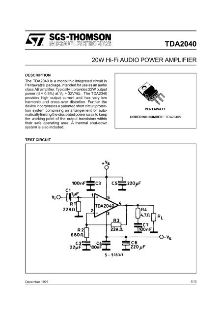
TDA2040<br />
<strong>20W</strong> Hi-Fi <strong>AUDIO</strong> <strong>POWER</strong> AMPLI<strong>FI</strong>ER<br />
DESCRIPTION<br />
The TDA2040 is a monolithic integrated circuit in<br />
Pentawatt® package,intended for use as an audio<br />
class AB amplifier. Typically it provides 22W output<br />
power (d = 0.5%) at V s = 32V/4Ω . The TDA2040<br />
provides high output current and has very low<br />
harmonic and cross-over distortion. Further the<br />
device incorporates a patented short circuit protection<br />
system comprising an arrangement for automaticallylimiting<br />
the dissipated powersoas to keep<br />
the working point of the output transistors within<br />
their safe operating area. A thermal shut-down<br />
system is also included.<br />
PENTAWATT<br />
ORDERING NUMBER : TDA2040V<br />
TEST CIRCUIT<br />
December 1995<br />
1/13
TDA2040<br />
SCHEMATIC DIAGRAM<br />
PIN CONNECTION<br />
THERMAL DATA<br />
Symbol Parameter Value Unit<br />
R th j-case Thermal Resistance Junction-case Max. 3 °C/W<br />
2/13
TDA2040<br />
ABSOLUTE MAXIMUM RATINGS<br />
Symbol Parameter Value Unit<br />
Vs Supply Voltage ± 20 V<br />
V i Input Voltage V s<br />
V i Differential Input Voltage ± 15 V<br />
Io Output Peak Current (internally limited) 4 A<br />
P tot Power Dissipation at T case =75°C 25 W<br />
T stg ,T j Storage and Junction Temperature – 40 to + 150 °C<br />
ELECTRICAL CHARACTERISTICS<br />
(refer to the test circuit, VS = ± 16V, Tamb =25 o C unless otherwise specified)<br />
Symbol Parameter Test Conditions Min. Typ. Max. Unit<br />
Vs Supply Voltage ± 2.5 ± 20 V<br />
I d Quiescent Drain Current V s = ± 4.5V<br />
Vs = ± 20V 45<br />
Ib Input Bias Current Vs = ± 20V 0.3 1 µA<br />
Vos Input Offset Voltage Vs = ± 20V ± 2 ± 20 mV<br />
I os Input Offset Current ± 200 nA<br />
P o Output Power d = 0.5%, T case =60°C<br />
f = 1kHz R L =4Ω<br />
R L =8Ω<br />
f = 15kHz RL =4Ω<br />
BW Power Bandwidth Po = 1W, RL =4Ω 100 kHz<br />
G v Open Loop Voltage Gain f = 1kHz 80 dB<br />
G v Closed Loop Voltage Gain f = 1kHz 29.5 30 30.5 dB<br />
d Total Harmonic Distortion P o = 0.1 to 10W, R L =4Ω<br />
f = 40 to 15000Hz<br />
f = 1kHz<br />
eN Input Noise Voltage B = Curve A<br />
B = 22Hz to 22kHz<br />
iN Input Noise Current B = Curve A<br />
B = 22Hz to 22kHz<br />
20<br />
15<br />
22<br />
12<br />
18<br />
0.08<br />
0.03<br />
30<br />
100<br />
2<br />
3 10<br />
50<br />
80 200<br />
Ri Input Resistance (pin 1) 0.5 5 MΩ<br />
SVR Supply Voltage Rejection R L =4Ω,R g = 22kΩ, G v = 30dB 40 50 dB<br />
f = 100Hz, Vripple = 0.5VRMS<br />
η Efficiency f = 1kHz<br />
%<br />
Po = 12W RL =8Ω<br />
66<br />
Po= 22W RL =4Ω<br />
63<br />
T j Thermal Shut-down Junction Temperature 145 °C<br />
mA<br />
mA<br />
W<br />
%<br />
µV<br />
µV<br />
pA<br />
3/13
TDA2040<br />
Figure 1 : Output Power versus Supply Voltage Figure 2 : Output Power versus Supply Voltage<br />
Figure 3 : Output Power versus Supply Voltage Figure 4 : Distortion versus Frequency<br />
Figure 5 :<br />
Supply Voltage Rejection versus<br />
Frequency<br />
Figure 6 :<br />
Supply Voltage Rejection versus<br />
Voltage Gain<br />
4/13
TDA2040<br />
Figure 7 :<br />
Quiescent Drain Current versus<br />
Supply Voltage<br />
Figure 8 :<br />
Open Loop Gain versus Frequency<br />
Figure 9 :<br />
Power Dissipation versus Output<br />
Power<br />
5/13
TDA2040<br />
Figure 10 : Amplifier with Split Power Supply<br />
Figure 11 : P.C. Board and Components Layout for the Circuit of Figure 10 (1:1 scale)<br />
6/13
TDA2040<br />
Figure 12 : Amplifier with Split Power Supply (see Note)<br />
Note : In this case of highly inductive loads protection diodes may be necessary.<br />
Figure 13 : P.C. Board and Components Layout for the Circuit of Figure 12 (1:1 scale)<br />
7/13
TDA2040<br />
Figure 14 : 30W Bridge Amplifier with Split Power Supply<br />
Figure 15 : P.C. Board and Components Layout for the Circuit of Figure 14 (1:1 scale)<br />
8/13
TDA2040<br />
Figure 16 : Two Way Hi-Fi System with Active Crossover<br />
Figure 17 : P.C. Board and Components Layout for the Circuit of Figure 16 (1:1 scale)<br />
9/13
TDA2040<br />
Figure 18 : Frequency Response Figure 19 : Power Distribution versus Frequency<br />
MULTIWAY SPEAKER SYSTEMS AND ACTIVE<br />
BOXES<br />
Multiway loudspeaker systems provide the best<br />
possible acoustic performance since each loudspeaker<br />
is specially designed and optimized to<br />
handle a limited range of frequencies. Commonly,<br />
these loudspeaker systems divide the audio spectrum<br />
into two, three or four bands.<br />
To maintain a flat frequencyresponseover the Hi-Fi<br />
audio range the bands covered by each loudspeaker<br />
must overlap slightly. Imbalance between<br />
the loudspeakers produces unacceptable results<br />
therefore it is important to ensure that each unit<br />
generates the correct amount of acoustic energy<br />
for its segment of the audio spectrum. In this respect<br />
it is also important to know the energy distribution<br />
of the music spectrum determine the cutoff<br />
frequenciesof the crossover filters (see Figure 19).<br />
As an example, a 100W three-way system with<br />
crossover frequencies of 400Hz and 3kHz would<br />
require 50W for the woofer, 35W for the midrange<br />
unit and 15W for the tweeter.<br />
Both active and passive filters can be used for<br />
crossovers but today active filters cost significantly<br />
less than a good passive filter using air-cored inductors<br />
and non-electrolyticcapacitors. In addition,<br />
active filters do not suffer from the typical defects<br />
of passive filters :<br />
- power loss<br />
- increased impedance seen by the loudspeaker<br />
(lower damping)<br />
- difficulty of precise design due to variable loudspeaker<br />
impedance<br />
Obviously, active crossovers can only be used if a<br />
power amplifier is provided for each drive unit. This<br />
makes it particularly interesting and economically<br />
sound to use monolithic power amplifiers. In some<br />
applications, complex filters are not really necessary<br />
and simple RC low-pass and high-pass networks<br />
(6dB/octave) can be recommended.<br />
The results obtained are excellent because this is<br />
the best type of audio filter and the only one free<br />
from phase and transient distortion.<br />
The rather poor out of band attenuation of single<br />
RC filters means that the loudspeaker must operate<br />
linearly well beyond the crossoverfrequency to<br />
avoid distortion.<br />
A more effective solution, named ”Active Power<br />
Filter” by SGS is shown in Figure 20.<br />
Figure 20 : Active Power Filter<br />
The proposed circuit can realize combined power<br />
amplifiers and 12dB/octave or 18dB/octave highpass<br />
or low-pass filters.<br />
In practice, at the input pins of the amplifier two<br />
equal and in-phase voltages are available, as required<br />
for the active filter operation.<br />
10/13
TDA2040<br />
The impedanceat the pin (-) is of the order of 100Ω,<br />
while that of the pin (+) is very high, which is also<br />
what was wanted.<br />
C1 = C2 = C3 R1 R2 R3<br />
22 nF 8.2 kΩ 5.6 kΩ 33 kΩ<br />
The component values calculated for f c = 900Hz<br />
using a Bessel 3rd order Sallen and Key structure<br />
are :<br />
In the block diagram of Figure 21 is represented an<br />
active loudspeaker system completely realized using<br />
power integrated circuit, rather than the traditional<br />
discrete transistors on hybrids, very high<br />
quality is obtained by driving the audio spectrum<br />
into three bands using active crossovers<br />
(TDA2320A) and a separate amplifier and loudspeakers<br />
for each band.<br />
A modern subwoofer/midrange/tweetersolution is<br />
used.<br />
PRATICAL CONSIDERATION<br />
Printed Circuit Board<br />
The layout shown in Figure 11 should be adopted<br />
by the designers. If different layouts are used, the<br />
ground points of input 1 and input 2 must be well<br />
decoupled from the gorund return of the output in<br />
which a high current flows.<br />
Assembly Suggestion<br />
No electrical isolation is needed between the package<br />
and the heatsink with single supply voltage<br />
configuration.<br />
Application Suggestions<br />
The recommended values of the components are<br />
those shown on application circuit of Fig. 10. Different<br />
values can be used. The following table can<br />
help the designer.<br />
Figure 21 : High Power Active LoudspeakerSystem using TDA2030A and TDA2040<br />
Comp.<br />
Recom.<br />
Value<br />
Purpose<br />
Larger than<br />
Recommended Value<br />
Smaller than<br />
Recommended Value<br />
R1 22kΩ Non inverting input biasing Increase of input impedance Decrease of input impedance<br />
R2 680Ω Closed loop gain setting Decrease of gain (*) Increase of gain<br />
R3 22kΩ Closed loop gain setting Increase of gain Decrease of gain (*)<br />
R4 4.7Ω Frequency stability Danger of oscillation at high<br />
frequencies with inductive loads<br />
C1 1µF Input DC decoupling Increase of low frequencies cut-off<br />
C2 22µF Inverting DC decoupling Increase of low frequencies cut-off<br />
C3, C4 0.1µF Supply voltage bypass Danger of oscillation<br />
C5, C6 220µF Supply voltage bypass Danger of oscillation<br />
C7 0.1µF Frequency stability Danger of oscillation<br />
(*) The value of closed loop gain must be higher than 24dB<br />
11/13
TDA2040<br />
PENTAWATT PACKAGE MECHANICAL DATA<br />
DIM.<br />
mm<br />
inch<br />
MIN. TYP. MAX. MIN. TYP. MAX.<br />
A 4.8 0.189<br />
C 1.37 0.054<br />
D 2.4 2.8 0.094 0.110<br />
D1 1.2 1.35 0.047 0.053<br />
E 0.35 0.55 0.014 0.022<br />
F 0.8 1.05 0.031 0.041<br />
F1 1 1.4 0.039 0.055<br />
G 3.4 0.126 0.134 0.142<br />
G1 6.8 0.260 0.268 0.276<br />
H2 10.4 0.409<br />
H3 10.05 10.4 0.396 0.409<br />
L 17.85 0.703<br />
L1 15.75 0.620<br />
L2 21.4 0.843<br />
L3 22.5 0.886<br />
L5 2.6 3 0.102 0.118<br />
L6 15.1 15.8 0.594 0.622<br />
L7 6 6.6 0.236 0.260<br />
M 4.5 0.177<br />
M1 4 0.157<br />
Dia 3.65 3.85 0.144 0.152<br />
L<br />
E<br />
A<br />
C<br />
L1<br />
D<br />
M M1<br />
D1<br />
L2<br />
L5<br />
L3<br />
H3<br />
G<br />
G1<br />
Dia.<br />
L7<br />
F1<br />
H2<br />
F<br />
L6<br />
12/13
TDA2040<br />
Information furnished is believed to be accurate and reliable. However, SGS-THOMSON Microelectronics assumes no responsibility for the<br />
consequences of use of such information nor for any infringement of patents or other rights of third parties which may result from its use. No<br />
license is granted by implication or otherwise under any patent or patent rights of SGS-THOMSON Microelectronics. Specifications mentioned<br />
in this publication are subject to change without notice. This publication supersedes and replaces all information previously supplied.<br />
SGS-THOMSON Microelectronics products are not authorized for use as critical components in life support devices or systems without express<br />
written approval of SGS-THOMSON Microelectronics.<br />
© 1996 SGS-THOMSON Microelectronics All Rights Reserved<br />
SGS-THOMSON Microelectronics GROUP OF COMPANIES<br />
Australia - Brazil - Canada - France - Germany - Hong Kong - Italy - Japan - Korea - Malaysia - Malta - Morocco - The Netherlands -<br />
Singapore - Spain - Sweden - Switzerland - Taiwan - Thaliand - United Kingdom - U.S.A.<br />
13/13