

a reliable wafer-level chip scale package (wlcsp) - AKRO Engineering
a reliable wafer-level chip scale package (wlcsp) - AKRO Engineering
a reliable wafer-level chip scale package (wlcsp) - AKRO Engineering

You also want an ePaper? Increase the reach of your titles
YUMPU automatically turns print PDFs into web optimized ePapers that Google loves.
A RELIABLE WAFER-LEVEL CHIP SCALE<br />
PACKAGE (WLCSP) TECHNOLOGY<br />
Umesh Sharma, Ph.D., Philip Holland and Harry Gee<br />
California Micro Devices, Inc.<br />
Milpitas, CA, USA<br />
umeshs@cmd.com, philh@cmd.com, and harryg@cmd.com<br />
Metin Ozen, Ph.D. and Can Ozcan<br />
Ozen <strong>Engineering</strong>, Inc.<br />
Sunnyvale, CA, USA<br />
Metin@ozeninc.com and can@ozeninc.com<br />
ABSTRACT<br />
In conventional WLCSP process, after defining the under<br />
bump metal (UBM) layer, a solder ball is dropped in the<br />
UBM opening. A subsequent thermal reflow cycle melts the<br />
solder ball and cools it in a well defined shape on top of the<br />
UBM layer. One draw back of this technology is the fracture<br />
or cracking of passivation film that may occur during the<br />
solder ball reflow process. The cracks in the passivation<br />
expose the underlying semiconductor devices to the ambient<br />
environment. Such cracks result in long term reliability<br />
problems or complete failure depending on the extent of the<br />
exposure to harmful ambient.<br />
In this paper, we systematically analyze the problem of<br />
passivation cracking and present a WLCSP process that is<br />
resistant to cracking during solder flow and subsequent<br />
multiple reflow steps. ANSYS thermo-mechanical finite<br />
element modeling software is used to model the WLCSP<br />
structure and process flow to evaluate stress and<br />
deformation at various points across the device structure.<br />
Contour plots clearly highlight the high stress regions and<br />
pinpoint the potential failure region. The use of ANSYS<br />
software in optimizing process parameters, and predicting<br />
reliability is presented. The experimental results confirm<br />
our simulation results and we conclude by presenting an<br />
optimized process that is resistant to passivation cracking<br />
and resulting failures.<br />
Keywords: WLCSP, passivation cracks, re-passivation,<br />
ANSYS, simulations<br />
INTRODUCTION AND PROBLEM DESCRIPTION<br />
WLCSP is a well established IC <strong>package</strong> technology. In its<br />
simplest form, the WLCSP process technology requires an<br />
under ball metallization layer (UBM) deposited and<br />
patterned over the passivation openings on a <strong>wafer</strong>.<br />
Subsequently, a solder ball is dropped through a stencil<br />
mask on the UBM stack. The <strong>wafer</strong> is then subjected to a<br />
thermal flow process in an oven. The thermal treatment<br />
melts the solder ball and cools it in a well defined shape as<br />
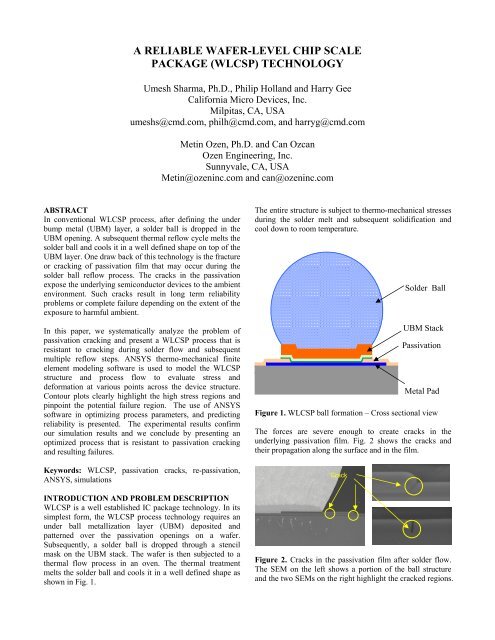
shown in Fig. 1.<br />
The entire structure is subject to thermo-mechanical stresses<br />
during the solder melt and subsequent solidification and<br />
cool down to room temperature.<br />
Figure 1. WLCSP ball formation – Cross sectional view<br />
The forces are severe enough to create cracks in the<br />
underlying passivation film. Fig. 2 shows the cracks and<br />
their propagation along the surface and in the film.<br />
Crack<br />
Solder Ball<br />
UBM Stack<br />
Passivation<br />
Metal Pad<br />
Figure 2. Cracks in the passivation film after solder flow.<br />
The SEM on the left shows a portion of the ball structure<br />
and the two SEMs on the right highlight the cracked regions.
These cracks left in the passivation film expose the<br />
underlying structures to the harmful ambient environment. It<br />
is quite easy for moisture and other contaminants to<br />
penetrate the device structures through the cracks leading to<br />
circuit failure. Besides environmental damage, the primary<br />
catastrophic failure is caused when the IC is assembled on<br />
the PC board using conventional SMT techniques. Standard<br />
procedures for mounting the ICs on a PC board require<br />
application of a “flux” and then a thermal cycle to melt the<br />
solder. It is during the flux application process, we have<br />
seen the most damage done to the IC. Figure 3 clearly<br />
highlights this problem. The flux can easily migrate through<br />
the crack and attack the metal pad or the metal wiring.<br />
Typical chemicals used in the flux are strong enough to<br />
corrode the metal and etch away selected portions of metal<br />
lines as shown in the bottom SEM in Figure 3.<br />
crack formation. We combined theoretical simulations with<br />
experimental results on carefully designed daisy chain<br />
structures to develop the best WLCSP process. In the<br />
following paragraphs we describe our experimental methods<br />
and highlight our major findings.<br />
THEORETICAL ANALYSIS –ANSYS SIMULATIONS<br />
To aid design of experiments and develop a deeper<br />
understanding of the failure mechanism, we created a finite<br />
element model of a WLCSP ball structure. Figure 4 shows a<br />
unit cell of the WLCSP structure. Finite Element Model is<br />
generated using APDL(Ansys Parametric Design Language)<br />
parametrically such that the dimensions, material properties,<br />
and loading conditions can be changed for subsequent<br />
simulations. Periodic boundary conditions are applied on the<br />
finite element model boundaries to model physics with the<br />
representative model. Material models are assumed to be<br />
linear elastic and isotropic for this analysis. Material<br />
properties used in the model are taken from the available<br />
sources in the web[1],[2]. The material names, and<br />
properties are presented in Table 1. Deposition process of<br />
different layers are carried out using the EKILL and<br />
EALIVE commands in Ansys which allow turning-off and<br />
turning-on of the active elements during simulations. This<br />
capability allows the deposition modeling of different<br />
materials at different temperatures. Reference temperature is<br />
taken as 25°C for the model, but the materials are activated<br />
at the elevated deposition temperatures such that the stress<br />
free state is achieved at the time of deposition.<br />
Figure 3. The flux used during PCB mounting of the IC,<br />
flows through the cracks (top) and etches away the<br />
Aluminum pad (bottom).<br />
Figure 4. Finite Element Model of a 0.5mm pitch WLCSP<br />
structure. Periodic boundary conditions are assumed.<br />
The location, density, and size of the cracks in the<br />
passivation film are dependent on several critical parameters.<br />
The solder reflow temperature, the composition of the UBM<br />
material, composition of the passivation films, the vertical<br />
and horizontal geometries of the ball structure, etc., are<br />
some of the parameters that affect passivation cracking.<br />
In this work we embarked upon understanding the<br />
relationship between all of the above factors and the<br />
composite thermo-mechanical stress produced in the<br />
passivation film during solder reflow. The goal was to arrive<br />
at an optimum WLCSP process that would be resistant to<br />
Table I. Mechanical and thermal properties of the materials<br />
used in the WLCSP structure model.
The finite element analysis simulates the thermal cycle<br />
during the entire process. The most relevant information is<br />
the 1 st principal stress before and after the solder flow<br />
thermal cycle. Both the magnitude and location of the stress<br />
vectors are important. In the next few paragraphs, we<br />
present path plots in the passivation layer, around the edge<br />
to extract stresses along this critical path and compare<br />
results for various simulation conditions. The top view of<br />
the path location for the WLCSP structure is shown in<br />
Figure 5.<br />
For all thickness values, the maximum stress values are<br />
around the region where the circular metal pad connects to<br />
the metal interconnects. For thinner nitride films, the stress<br />
is highly non-uniform ranging from very high values near<br />
the interconnect regions versus very low values further<br />
away. As the thickness increases, the average stress rises<br />
throughout the film but the peak stress actually reduces.<br />
This is an important finding as it suggests a possibility of<br />
optimizing the stress <strong>level</strong> in the passivation film by<br />
choosing the right thickness.<br />
X<br />
Y<br />
<br />
Figure 5. Top view of the WLCSP structure. The dashed<br />
line shows the path of 1 st principal stress near the edge of<br />
the passivation layer.<br />
Simulations were performed in several batches, varying one<br />
process parameter at a time and evaluating the impact of the<br />
variation on the final stress. An example of such a<br />
simulation is the study of the effect of gradually increasing<br />
the nitride passivation thickness. The nitride thickness was<br />
varied from 8KÅ to 20KÅ in steps of 2KÅ. The results of<br />
the principal stress calculations are plotted in Fig. 6.<br />
Figure 7. Principal stress along the cracking path. As the<br />
path location (a) is varied, the stress increases or decreases<br />
depending on the location. Peak stress is observed at the<br />
pad connection to the metal lines. Average stress rises with<br />
film thickness but peak stress reduces with increasing<br />
thickness.<br />
We ran several simulations and were able to predict both<br />
qualitative and quantitative stress <strong>level</strong>s in the passivation<br />
film after completion of the WLCSP process. Results from<br />
key simulation runs are presented below in Figures. 8-11.<br />
Figure 8. Principal stress along the cracking path. In this<br />
experiment a dual dielectric passivation film (oxide +<br />
nitride) was chosen. The figure compares 4 different cases:<br />
1) original 12KÅ nitride, 2) Case-1 6K oxide + 6K nitride,<br />
3) Case-2 8KÅ oxide + 6KÅ nitride, and 4) Case-3 12KÅ<br />
oxide + 6KÅ nitride. Clearly, both peak and average stress<br />
values can be reduced by using a dual dielectric film of<br />
oxide + nitride instead of the nitride film alone.<br />
Figure 6. The stress in the passivation film is shown as a<br />
function of the nitride thickness. The stress value increases<br />
in the color coded charts from blue to red.
under the nitride, adding a polyimide layer on top of<br />
passivation or by carefully tailoring the design rules.<br />
Based on these findings and our anticipation that reduced<br />
cumulative stress would lead to less fatigue and eventually<br />
fewer cracks in the passivation film, we narrowed down our<br />
experimental matrix to just a few parameters. In the<br />
following section we discuss the experimental procedure<br />
and the results of various experiments.<br />
Figure 9. Principal stress along the cracking path. In this<br />
simulation run comparison is made between two WLCSP<br />
processes (0.4mm ball pitch vs. 0.5mm ball pitch). We<br />
observe higher peak stress for the 0.4mm ball pitch case.<br />
This suggests different optimizations for these two<br />
processes.<br />
EXPERIMENTAL PROCEDURES AND RESULTS<br />
Experimental Procedures<br />
To facilitate detailed study of this phenomenon and simply<br />
the analysis, we designed a 5x5 daisy chain with 5 rows and<br />
5 columns of I/Os linked with metal as shown in Figure 12.<br />
After WLCSP processing, the daisy chains were mounted<br />
on a FR-4 board designed to complete the electrical<br />
continuity between the two ends of the chain. Resistance<br />
was measured after mounting the parts on the board. A<br />
crack in the passivation layer would lead to flux going<br />
through the crack and attacking the metal lines underneath.<br />
Failed parts would typical register an “OPEN” or “High<br />
Resistance”.<br />
Figure 10. Principal stress along the cracking path. In this<br />
simulation run, the UBM opening and the metal pad<br />
diameter are varied to study the dependence on layout rules.<br />
Comparing 3 different cases: 1) Original UBM opening =<br />
240um + Pad size = 260um, 2) Case-1 UBM = 240um +<br />
Pad size = 290um, 3) Case-2 UBM = 210um + Pad size =<br />
260um. Peak stress is lower for Case-1 and Case-2.<br />
Figure 12. Daisy chain layout<br />
Figure 11. Principal stress along the cracking path. In this<br />
simulation, addition of a polyimide coat over the passivation<br />
layer is investigated. Stress can be reduced significantly by<br />
adding the polyimide layer. Three cases are considered: 1)<br />
original – no polyimide, 2) Case-1 10um of polyimide, and<br />
3) Case-2 3um of polyimide.<br />
The simulation results above point to a complex relationship<br />
between the passivation film stress and various process and<br />
layout parameters. In general, stress can be reduced by<br />
increasing the nitride thickness, adding a pad oxide layer<br />
In a typical 2-sided FR4 board mounting process the IC is<br />
subjected to 2 solder reflows. We also subjected a few parts<br />
to additional 3X reflows with the same temperature profile<br />
as the standard lead free WLCSP mount process. Daisy<br />
chains were visually examined before and after reflows for<br />
any signs of passivation cracks. Daisy chains were also<br />
electrically measured before and after reflows to examine<br />
metal continuity.<br />
Process Experiments<br />
Wafers were split into several groups. Main process<br />
experiments can be summarized as follows:<br />
1) Nitride thickness variation – 6KÅ, 9KÅ, 12KÅ,<br />
15KÅ, 18KÅ<br />
2) Nitride vs. Oxynitride – 12KÅ
3) Oxide + Nitride dual dielectric (6KÅ/6KÅ,<br />
6KÅ/12KÅ, 12KÅ/6KÅ)<br />
4) Deposition Tool A vs. Deposition Tool B (12KÅ<br />
nitride, 6KÅ oxide + 12KÅ nitride)<br />
5) No polyimide vs. Polyimide (10um)<br />
The primary goal of these experiments was to design a<br />
WLCSP vertical structure that is free of cracks in the<br />
passivation immediately after processing and can withstand<br />
3X thermal reflow cycles. After WLCSP processing, one<br />
<strong>wafer</strong> from every group was used for visual examination<br />
under a high power microscope. The solder balls were<br />
chemically removed from the <strong>wafer</strong> to allow observations of<br />
cracks in the passivation underneath the balls. Rest of the<br />
<strong>wafer</strong>s were diced and the individual ICs were mounted on<br />
the FR-4 board. The devices were then subjected to 3X<br />
reflows using the same temperature profile as the SMT<br />
assembly process. Daisy chains were electrically measured<br />
after completion of the 3X reflow.<br />
EXPERIMENTAL RESULTS<br />
Results after 3X reflow cycle provide the most dramatic<br />
contrast among various <strong>wafer</strong> groups. These results are<br />
summarized in Table 2.<br />
No. Passivation<br />
% Failed Pads<br />
After 3X Reflow<br />
1 6KÅ SiN 98.00%<br />
2 6 KÅ SiO2 + 6 KÅ SiN 39.60%<br />
3 12 KÅ SiO2 + 6 KÅ SiN 59.33%<br />
4 9 KÅ SiN 5.60%<br />
5 12k SiN 0.24%<br />
6 6 KÅ SiO2 + 12 KÅ SiN 0.02%<br />
7 15 KÅ SiN 8.80%<br />
8 18 KÅ SiN 0.22%<br />
9 12 KÅ SiON 96.40%<br />
10 6 KÅ SiO2 + 12 KÅ SiON 10.00%<br />
11 12 KÅ SiN(Deposition tool B) 0.02%<br />
12 6 KÅ SiO2+12 KÅ SiN 0%<br />
(Deposition Tool B )<br />
13 12 KÅ SiN + 10um Polyimide 0%<br />
14 6 KÅ SiO2+12 KÅ SiN + 0%<br />
10um Polyimide<br />
Table 2. Summary of experimental results<br />
Upon examining the table carefully we can draw the<br />
following conclusions:<br />
A) SiN passivation thickness: Examining <strong>wafer</strong><br />
groups 1, 4, 5, and 8, we can see a definite<br />
correlation with nitride thickness as predicted by<br />
the simulations. From Figure7, we observe a<br />
reduction in the peak stress with increasing nitride<br />
thickness. The experimental results are consistent<br />
with this observation. For 6KÅ nitride film, the<br />
failure rate is as high as 98% but for 18KÅ nitride<br />
film, the failure rate drops to 0.22%.<br />
B) Comparing SiN passivation with Oxynitride<br />
passivation: Group 5 and Group 9 comparison<br />
shows that a single oxynitride film is worse than<br />
the nitride film of same thickness.<br />
C) Dual Dielectric passivation film (SiO2 + SiN): A<br />
comparison of groups 2 and 3 shows that both<br />
groups have high failure rate. Thus, increasing the<br />
oxide thickness does not prevent cracking. But,<br />
comparing 2 and 3 with group 6 suggests the<br />
dramatic improvement in performance obtained by<br />
increasing the nitride film in the stack to 12KÅ.<br />
The failure rate for group 6 is only 0.02%. Using<br />
Oxynitride as the second film instead of nitride<br />
makes matters worse. The failure rate for group 10<br />
increases to 10%.<br />
D) Effect of nitride deposition tool: Experimental<br />
data show that Deposition Tool B is marginally<br />
better than Deposition Tool A as evidenced by<br />
comparing Group 5 and Group 12. This result is<br />
due to minor differences in deposition conditions<br />
such as gas flow, pressure, and chamber design.<br />
E) The Optimal results: From the table it is clear that<br />
the best results are for the case when the<br />
passivation film is a composite insulator consisting<br />
of 6KÅ SiO2 + 12KÅ SiN. The failure rate is zero<br />
(within statistical limits) for this combination,<br />
especially if the nitride is deposited using<br />
Deposition Tool B.<br />
We also investigated the effect of a 10um thick polyimide<br />
layer deposited on top of the passivation layer. This process<br />
is known in the industry as “Re-passivation WLCSP”<br />
process. Schematically, the resulting vertical ball structure is<br />
shown in Figure 13.<br />
Solder<br />
UBM<br />
Polyimide<br />
Passivation<br />
Metal<br />
Figure 13. “Re-passivation WLCSP” ball formation –<br />
Cross sectional view. A thick polyimide layer is added on<br />
top of the passivation film before ball drop.<br />
Addition of the thick polyimide layer completely prevents<br />
any failures due to thermo-mechanical stresses during<br />
processing or PC board assembly. Because polyimide has a<br />
higher coefficient of thermal expansion (52ppm/K) and
much lower Young’s modulus than either oxide or nitride<br />
films with a CTE of (0.75 – 2.8ppm/K) and Young’s<br />
modulus (68 – 290 GPa) (see Table 1), it provides larger<br />
elongation and therefore a “cushioning effect” during<br />
WLCSP process or subsequent reflow steps. Even if the<br />
passivation underneath cracks due to thermal fatigue, the<br />
polyimide film covers up all the cracks and seals all the<br />
cracks. In this manner, the corrosive flux or any other<br />
harmful ambient element are unable to enter the cracks and<br />
cause damage. The SEM shown in Figure 14, illustrates this<br />
result.<br />
Figure 14. Addition of a thick polyimide layer (top row) to<br />
prevent flux migration.<br />
CONCLUSIONS<br />
In this paper we discussed a commonly observed problem<br />
for all WLCSP products. Various compressive and tensile<br />
forces present during solder flow and subsequent cooling<br />
cycle cause cracks in the passivation film. These cracks<br />
expose the underlying circuitry to harmful ambient<br />
chemicals and volatile compounds during assembly process<br />
and can cause circuit failure.<br />
The best method of preventing assembly failures due to<br />
these cracks is to add a thick layer of polyimide on top of<br />
the passivation film. However, the polyimide layer increases<br />
the manufacturing cost. A second approach requires<br />
optimization of the composition, thickness, and deposition<br />
conditions of the passivation film. Passivation cracks can be<br />
minimized or completely eliminated by using a dual<br />
dielectric layer passivation consisting of oxide and nitride<br />
films. The best results are obtained by using a 6KÅ thick<br />
oxide layer followed by a 12KÅ thick nitride layer.<br />
ACKNOWLEDGEMENTS<br />
The authors would like to thank Sanyo Semiconductor, Inc. ,<br />
and JCAP, Inc., who were involved in supporting this study.<br />
The authors would also like to acknowledge the support of<br />
CMD management in this study, in particular Manny Mere<br />
and Bob Dickinson.<br />
REFERENCES<br />
[1] www.matweb.com.<br />
[2]http://www.flip<strong>chip</strong>.com/get_started/FCI_bump_design_<br />
guide.pdf


![Moldflow Adviser Giriş Eğitimi Broşürü [2 gün] - AKRO Engineering](https://img.yumpu.com/3939177/1/190x245/moldflow-adviser-giris-egitimi-brosuru-2-gun-akro-engineering.jpg?quality=85)