Auto SE New - Horiba
Auto SE New - Horiba
Auto SE New - Horiba

You also want an ePaper? Increase the reach of your titles
YUMPU automatically turns print PDFs into web optimized ePapers that Google loves.
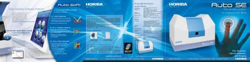
"User Oriented Software Platform"<br />
The fully automatic mode provides<br />
a very intuitive software based<br />
on the use of icons. Four main<br />
interfaces are available to build<br />
experimental recipes, manage<br />
data, control the system in realtime,<br />
and for maintenance.<br />
DeltaPsi2 Scientific Mode<br />
to Extend the Measurement<br />
Capability<br />
DeltaPsi2 is a fully integrated<br />
spectroscopic ellipsometry<br />
platform that includes advanced<br />
measurement and analysis<br />
capabilities and a complete<br />
materials database.<br />
This software is ideal for<br />
engineering applications for new<br />
sample characterization or<br />
optimization of an existing<br />
experimental recipe. Once the<br />
new recipe is validated it can be<br />
performed repeatedly without<br />
expert intervention.<br />
<strong>Auto</strong> Soft<br />
Fully <strong>Auto</strong>matic Mode<br />
for Routine Analysis<br />
1> Load Sample<br />
• <strong>Auto</strong>matic adjustment of the sample<br />
• Visualization of the spot on the sample<br />
with the My<strong>Auto</strong>View vision system<br />
• Choose your measurement site<br />
2> Run Measurement<br />
• Select your experimental recipe<br />
in the ready to use application database<br />
• Push the Run button<br />
• Measure at a single position or<br />
multiple positions to map thin<br />
film uniformity<br />
3> Accurate Results<br />
• Clear table provides thickness,<br />
optical constants, film uniformity<br />
and other material properties<br />
of the sample<br />
• Thin film result status:<br />
in or out tolerance limits<br />
• <strong>Auto</strong>matic reporting<br />
• Reprocessing capability<br />
Worldwide Customer Support<br />
Founded nearly 190 years ago, HORIBA Jobin Yvon is one of world’s largest manufacturers<br />
of analytical and spectroscopic systems and components. Certified ISO<br />
9001 and 14001, our instruments are manufactured under a strict quality assurance<br />
program. They are supported by a worldwide network of strategically located facilities<br />
in the United States, Europe and Asia that are ready to provide assistance when<br />
and where it is needed.<br />
Our staff of highly trained service and application specialists install and certify instrument<br />
performance, and conduct technical and application user training for smooth<br />
and efficient commissioning of the instruments.<br />
This commitment to product excellence and continued support is part of the<br />
HORIBA Jobin Yvon culture.<br />
<strong>Auto</strong> <strong>SE</strong> Awards<br />
2008 IC Industry<br />
<strong>New</strong> System Award<br />
2008 ACCSI Best <strong>New</strong><br />
Instrument of the Year<br />
Find us at www.horiba.com/scientific or contact us:<br />
France : HORIBA Jobin Yvon S.A.S., Z.I. La Vigne aux Loups, 5 avenue Arago, 91380 Chilly-Mazarin<br />
Tel: +33 (0)1 64 54 13 00 - Fax: +33 (0)1 69 74 88 61 - Email: info-sci.fr@horiba.com<br />
USA : HORIBA Jobin Yvon Inc., 3880 Park Avenue, Edison, NJ 08820-3012. Toll-free: +1-866-jobinyvon<br />
Tel: +1 732 494 8660 - Fax: +1 732 549 5125 - Email: info-sci.us@horiba.com<br />
Japan : HORIBA Ltd., Scientific Instruments Sales Dept., Alte Building Higashi-Kanda, 1-7-8 Higashi-Kanda,<br />
Chiyoda-ku, 101-0031 Tokyo - Tel: +81 (0)3 3861 8231 - Fax: +81 (0)3 3861 8259 - Email: info-sci.jp@horiba.com<br />
Germany : +49 (0)89 46 23 170 Italy: +39 02 57 60 30 50 UK: +44 (0)20 8204 8142<br />
China : +86 (0)10 8567 9966 Other countries: +33 (0)1 64 54 13 00 Korea: +82 (0)2 753 7911<br />
www.horiba.com/scientific<br />
<strong>Auto</strong> <strong>SE</strong> Specifications<br />
Standard Configuration<br />
Light source Combination halogen and blue LED<br />
Spectral range 440 – 1000 nm<br />
Spot size<br />
500 µm x 500 µm; 250 µm x 500 µm;<br />
250 µm x 250 µm; 70 µm x 250 µm;<br />
100 µm x 100 µm; 50 µm x 60 µm; 25 µm x 60 µm<br />
Detector<br />
CCD – Resolution: 2 nm<br />
Sample stage 200 mm x 200 mm, automatic XYZ adjustment,<br />
vacuum chuck, Z height 40 mm<br />
Sample viewing CCD camera – Field of view: 1.33*1 mm<br />
Resolution: 10 µm<br />
Goniometer Fixed at 70° - Possible set up at 66° or 61.5°<br />
Options<br />
Accessories<br />
• Sample cells: Temperature controlled cell,<br />
Electrochemical cell, Liquid cell<br />
• Sample stage: <strong>Auto</strong>sampler, 360° Rotation<br />
control, Transmission mount, Plastic film<br />
mounts, Lens and curved sample mounts<br />
Microspot Xenon lamp needed for spot sizes < 100 x 100 µm<br />
Table<br />
Dimension (wxdxh): 1400-1840 x 530 x 740 mm<br />
Performance<br />
Measurement time < 1 s, typical 5 s<br />
Accuracy NIST 1000 Å SiO 2<br />
/Si: d ± 4 Å - n(632.8 nm) ± 0.002<br />
Fused silica: n ± 0.004<br />
Repeatability ± 0.2 Å – Tested on NIST 150 Å SiO 2<br />
/Si<br />
Facility Requirements<br />
Operating systems Windows ® 2000 / XP / Vista / 7<br />
Power supply 100 V / 115 V / 230 V; 200 W; 50 / 60 Hz<br />
Weight<br />
80 kg<br />
Certificate<br />
CE<br />
592 mm<br />
572 mm<br />
760 mm<br />
Technology: Spectroscopic Ellipsometer, liquid crystal modulation based<br />
This document is not contractually binding under any circumstances - Printed in France - ©HORIBA Jobin Yvon - RCS EVRY B 837 150 366 - July 2010.<br />
<strong>Auto</strong> <strong>SE</strong><br />
The simple solution<br />
to measure thin films<br />
Film thickness,<br />
Optical constants,<br />
and Imaging
<strong>Auto</strong> <strong>SE</strong><br />
“Designed for your thin film measurements,<br />
to deliver maximum efficiency with simplicity”<br />
The <strong>Auto</strong> <strong>SE</strong> is a new thin film measurement tool that provides fully<br />
automated analysis of thin film samples with simple, push button<br />
operations.<br />
Sample analysis takes only a few seconds and a complete report is generated<br />
automatically. The report provides a comprehensive description of the thin film<br />
stack over the wavelength range 440-1000 nm, and includes film thicknesses,<br />
optical constants, surface roughness, and film inhomogeneities.<br />
The <strong>Auto</strong> <strong>SE</strong> includes numerous automatic features, and the patented<br />
My<strong>Auto</strong>View vision system allows the user to measure at exactly the right place<br />
every time.<br />
The <strong>Auto</strong> <strong>SE</strong> is a turnkey instrument ideal for routine thin film<br />
measurement and device quality control.<br />
Thin Film Analysis Made Easy<br />
• Ready-to-use system configured to meet your specific application needs<br />
• Full automatic analysis of thin film samples with simple push button operations<br />
• Comprehensive display results with automatic reporting and compliance<br />
• Multilanguage software<br />
“Optimized for enhanced functionality and flexibility”<br />
My<strong>Auto</strong>View Vision System<br />
• Visualization of the measurement site for all kinds of sample<br />
• Exact positioning of the measurement spot on a sample<br />
• Unique advantage for measurement of transparent substrates<br />
• Integrated microspot optics<br />
Highly Featured System<br />
• <strong>Auto</strong>matic sample loading and adjustment<br />
• <strong>Auto</strong>matic sample mapping<br />
• Fast measurement from 440-1000 nm < 1s<br />
• <strong>Auto</strong>mated selection of seven spot sizes<br />
• Accessories to suit all applications<br />
Intelligent Diagnostics<br />
• Detect and diagnose problems automatically<br />
with comprehensive operator guidance for<br />
troubleshooting<br />
• Stage with integrated reference samples for<br />
instrument quality control<br />
• Simple instrument maintenance<br />
Semiconductors<br />
• LED<br />
• Dielectrics<br />
• Thin metal films<br />
• Polymers, photoresists<br />
• Silicon<br />
• PZT<br />
• Laser diodes: GaN, AlGaN<br />
• Transparent electronics<br />
Flat Panel<br />
Displays<br />
• TFT<br />
• OLED<br />
• Plasma display panel<br />
• Flexible display<br />
Photovoltaic<br />
Devices<br />
• Amorphous, poly, micro, nano<br />
crystalline silicon<br />
• Transparent conducting oxides<br />
• Anti-reflective coatings<br />
• Organic materials<br />
Functional<br />
Coatings<br />
• Optical coatings: Anti<br />
reflective, self-cleaning,<br />
electrochromic, mirrors<br />
• Surface coatings and<br />
treatments: polymers,<br />
oil, Al 2<br />
O 3<br />
Biological and<br />
Chemical<br />
Engineering<br />
• Organic films, LB, SAM, protein<br />
• Film adsorption<br />
• Surface functionalization<br />
• Liquids<br />
Broad Range<br />
of Thin Film Applications<br />
Interfacial Behavior<br />
• Interface thickness<br />
• Composition of mixed materials forming interface<br />
• Monitor interface thickness in real-time:<br />
film growth, film adsorption<br />
• Monitor real-time changes at interfaces<br />
Surface<br />
Interface<br />
Thickness Measurement<br />
• From a few Å to 15 µm<br />
• Single and multi layers<br />
Material Properties<br />
• Graded and anisotropic film<br />
• Film porosity expressed in<br />
void percentage<br />
Surface Measurement<br />
Film<br />
• Roughness thickness<br />
• Native oxide thickness<br />
• Any surface film thickness<br />
• Depolarization coefficient<br />
Substrate<br />
Optical Properties<br />
• Optical constants (n,k) and <br />
• Optical bandgap Eg<br />
• Transmittance