experiment 6: flip-flops and feedback devices - The Circuits and ...
experiment 6: flip-flops and feedback devices - The Circuits and ...
experiment 6: flip-flops and feedback devices - The Circuits and ...

Create successful ePaper yourself
Turn your PDF publications into a flip-book with our unique Google optimized e-Paper software.
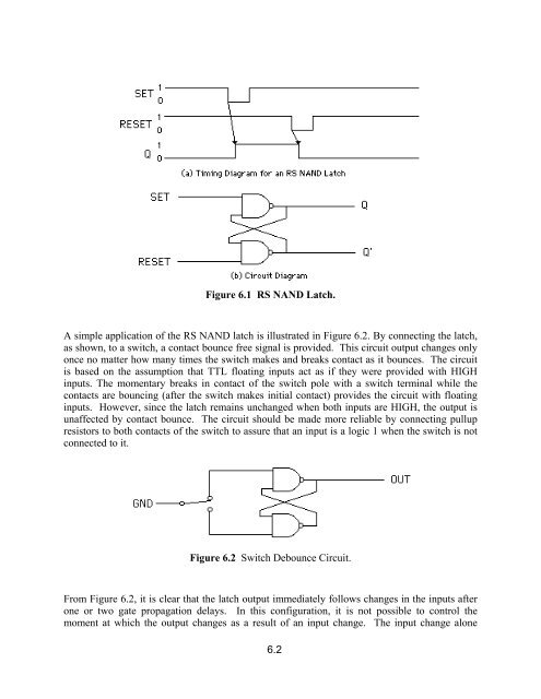
Figure 6.1 RS NAND Latch.<br />
A simple application of the RS NAND latch is illustrated in Figure 6.2. By connecting the latch,<br />
as shown, to a switch, a contact bounce free signal is provided. This circuit output changes only<br />
once no matter how many times the switch makes <strong>and</strong> breaks contact as it bounces. <strong>The</strong> circuit<br />
is based on the assumption that TTL floating inputs act as if they were provided with HIGH<br />
inputs. <strong>The</strong> momentary breaks in contact of the switch pole with a switch terminal while the<br />
contacts are bouncing (after the switch makes initial contact) provides the circuit with floating<br />
inputs. However, since the latch remains unchanged when both inputs are HIGH, the output is<br />
unaffected by contact bounce. <strong>The</strong> circuit should be made more reliable by connecting pullup<br />
resistors to both contacts of the switch to assure that an input is a logic 1 when the switch is not<br />
connected to it.<br />
Figure 6.2 Switch Debounce Circuit.<br />
From Figure 6.2, it is clear that the latch output immediately follows changes in the inputs after<br />
one or two gate propagation delays. In this configuration, it is not possible to control the<br />
moment at which the output changes as a result of an input change. <strong>The</strong> input change alone<br />
6.2