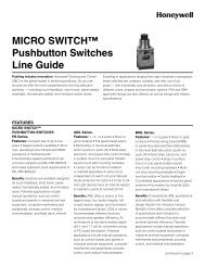
Infrared Sensors Line Guide - Honeywell Sensing and Control
Infrared Sensors Line Guide - Honeywell Sensing and Control
Infrared Sensors Line Guide - Honeywell Sensing and Control

Create successful ePaper yourself
Turn your PDF publications into a flip-book with our unique Google optimized e-Paper software.
SD3443.<br />
Features:TO-46 metal-can package • Flat<br />
window • 90° acceptance angle option<br />
• Wide operating temperature range -55<br />
°C to 125 °C [-67 °F to 257 °F] • External<br />
base connection for added control •<br />
Enhanced sensitivity • Mechanically <strong>and</strong><br />
spectrally matched to SE3450/5450,<br />
SE3455/5455, <strong>and</strong> SE3470/5470 infrared<br />
emitters<br />
Benefits: Phototransistor. Flat window<br />
provides wide acceptance angle. Often<br />
ideally suited for operation in hostile<br />
environments.<br />
SD5443.<br />
Features: TO-46 metal-can package<br />
• Lensed package • 18° (nominal)<br />
acceptance angle option • Wide operating<br />
temperature range -55 °C to 125 °C [-67<br />
°F to 257 °F] • External base connection<br />
for added control • Enhanced sensitivity<br />
• Mechanically <strong>and</strong> spectrally matched<br />
to SE3450/5450, SE3455/5455, <strong>and</strong><br />
SE3470/5470 infrared emitters<br />
Benefits: Phototransistor. Glass-lensed<br />
can provides a narrow acceptance angle.<br />
Often ideally suited for operation in hostile<br />
environments.<br />
SD5491.<br />
Features: TO-18 metal-can package<br />
• 12° (nominal) acceptance angle • Wide<br />
operating temperature range -55 °C to 125<br />
°C [-67 °F to 257 °F] • Enhanced response<br />
time • Wide sensitivity ranges • External<br />
base connection for added control<br />
• Mechanically <strong>and</strong> spectrally matched<br />
to SE3450/5450, SE3455/5455, <strong>and</strong><br />
SE3470/5470 infrared emitters<br />
Benefits: Phototransistor. Biconvex lens<br />
provides high optical sensitivity with<br />
a narrow acceptance angle to enable<br />
maximum radiation coupling. Often offers<br />
protection against harsh environments, as<br />
well as enhanced thermal characteristics.<br />
PHOTOTRANSISTORS - PLASTIC<br />
AND CERAMIC PACKAGE<br />
SDP8405.<br />
Features: T-1 plastic package • 20°<br />
(nominal) acceptance angle • Consistent<br />
optical properties • Wide sensitivity<br />
ranges • Mechanically <strong>and</strong> spectrally<br />
matched to SEP8505 <strong>and</strong> SEP8705<br />
infrared emitters<br />
Benefits: Phototransistor. Transfer molding<br />
provides enhanced optical centerline<br />
performance compared to other molding<br />
processes. Lead lengths are staggered<br />
to provide a simple method of polarity<br />
identification.<br />
SDP8406.<br />
Features: Side-looking plastic package<br />
• 50° (nominal) acceptance angle<br />
• Wide sensitivity ranges • Mechanically<br />
<strong>and</strong> spectrally matched to SEP8506 <strong>and</strong><br />
SEP8706 infrared emitters<br />
Benefits: Phototransistor molded in a<br />
side-looking clear plastic package. Chip<br />
positioned to accept radiation through a<br />
plastic lens from the side of the package.<br />
SDP8436.<br />
Features: Side-detecting, tight-beam<br />
sidelooker in a plastic package • 18°<br />
(nominal) acceptance angle • Enhanced<br />
coupling distance • Internal visible light<br />
rejection filter • Low profile for design<br />
flexibility • Wide sensitivity ranges<br />
• Mechanically matched to SEP8736<br />
infrared emitters<br />
Benefits: Phototransistor molded<br />
in a black plastic package which<br />
combines the mounting advantages of<br />
a side-looking package with the narrow<br />
acceptance angle <strong>and</strong> high optical<br />
gain of a T-1 package. Designed for<br />
potential applications with longer coupling<br />
distances than st<strong>and</strong>ard side-looking<br />
devices, such as touch screens. Often<br />
suited to potential applications in which<br />
adjacent channel cross-talk could be a<br />
problem. Package is highly transmissive<br />
to the IR source energy while effectively<br />
shielding against visible ambient light.<br />
SMD2440.<br />
Features: Small ceramic package size<br />
• Glass-lensed optics for efficient optical<br />
coupling • Upright or inverted mounting<br />
capability • Low profile, small size for<br />
flexible layout of multiple channels<br />
<strong>and</strong> custom arrays • Compatible with<br />
automated solder processes • Choice of<br />
photodiode or phototransistor detectors<br />
• <strong>Infrared</strong> emitter features high power<br />
dissipation capability • Tape <strong>and</strong> reel<br />
packaging option (pick <strong>and</strong> place<br />
machine compatible)<br />
Benefits: Lens minimizes cross-talk <strong>and</strong><br />
often eliminates the need for apertures<br />
in non-critical applications. Low profile<br />
components may be mounted on<br />
the printed circuit board, lens up or<br />
inverted, allowing flexibility in layouts<br />
for multiple channel <strong>and</strong> custom arrays.<br />
Phototransistor’s gain characteristics often<br />
make it useful for potential applications<br />
requiring high responsivity. Potential<br />
applications include optical encoders<br />
for motion control, computer peripherals,<br />
vending <strong>and</strong> point-of-sale applications,<br />
smoke detectors, <strong>and</strong> medical equipment.<br />
ENCODER DETECTORS<br />
HLC2701.<br />
Features: Side-looking plastic package<br />
• TTL/LSTTL/CMOS compatible • Senses<br />
speed <strong>and</strong> direction of mechanical motion<br />
• Inverting logic output • <strong>Line</strong>ar or rotary<br />
encoder applications • Resolution to<br />
0,229 mm [0.009 in] • Sensitivity versus<br />
temperature compensation • Mechanically<br />
<strong>and</strong> spectrally matched to SEP8506 <strong>and</strong><br />
SEP8706 infrared emitters<br />
Benefits: Monolithic IC, consisting of two<br />
narrow adjacent photodiodes, amplifiers,<br />
<strong>and</strong> Schmitt trigger output stages.<br />
Outputs are NPN collectors with internal<br />
10 kOhm (nominal) pull-up resistors to<br />
Vcc which can directly drive TTL loads.<br />
Circuitry compensates the sensitivity for<br />
the output power versus temperature<br />
characteristics of an infrared emitter. IC is<br />
encapsulated in a molded, unlensed black<br />
Unless otherwise noted, potential applications include printers <strong>and</strong> copiers, motion control systems, metering systems, liquid-level<br />
sensing, data storage systems, scanning, automated transaction, drop sensors, <strong>and</strong> other noninvasive medical equipment.<br />
16 www.honeywell.com/sensing