Insights into the Nano World: 40 Years of
Insights into the Nano World: 40 Years of
Insights into the Nano World: 40 Years of

Create successful ePaper yourself
Turn your PDF publications into a flip-book with our unique Google optimized e-Paper software.
Anniversary<br />
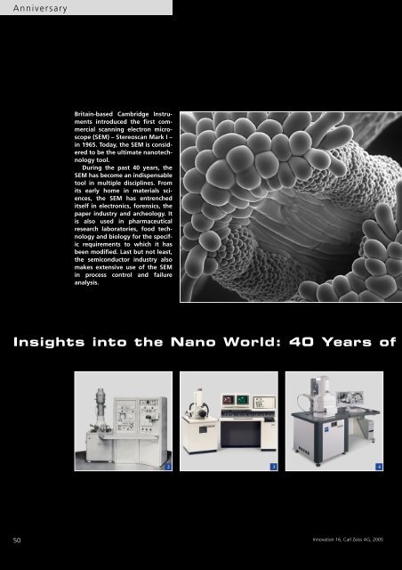
Britain-based Cambridge Instruments<br />
introduced <strong>the</strong> first commercial<br />
scanning electron microscope<br />
(SEM) – Stereoscan Mark I –<br />
in 1965. Today, <strong>the</strong> SEM is considered<br />
to be <strong>the</strong> ultimate nanotechnology<br />
tool.<br />
During <strong>the</strong> past <strong>40</strong> years, <strong>the</strong><br />
SEM has become an indispensable<br />
tool in multiple disciplines. From<br />
its early home in materials sciences,<br />
<strong>the</strong> SEM has entrenched<br />
itself in electronics, forensics, <strong>the</strong><br />
paper industry and archeology. It<br />
is also used in pharmaceutical<br />
research laboratories, food technology<br />
and biology for <strong>the</strong> specific<br />
requirements to which it has<br />
been modified. Last but not least,<br />
<strong>the</strong> semiconductor industry also<br />
makes extensive use <strong>of</strong> <strong>the</strong> SEM<br />
in process control and failure<br />
analysis.<br />
<strong>Insights</strong> <strong>into</strong> <strong>the</strong> <strong>Nano</strong> <strong>World</strong>: <strong>40</strong> <strong>Years</strong> <strong>of</strong><br />
2 3 4<br />
50<br />
Innovation 16, Carl Zeiss AG, 2005
1<br />
Scanning Electron Microscopy<br />
Ongoing development<br />
Ongoing development has resulted in<br />
entirely new functions since <strong>the</strong> first<br />
scanning electron microscopes were<br />
introduced. Two <strong>of</strong> <strong>the</strong>se new developments<br />
are exceptionally important:<br />
<strong>the</strong> development <strong>of</strong> <strong>the</strong> ZEISS<br />
GEMINI ® column in 1992, giving a<br />
boost to resolution, and <strong>the</strong> combination<br />
<strong>of</strong> <strong>the</strong> SEM column with a<br />
focused ion beam (FIB) column,<br />
transforming <strong>the</strong> instrument <strong>into</strong> a<br />
multi-versatile analysis system. This<br />
new system, CrossBeam ® , provides<br />
entirely new insights <strong>into</strong> <strong>the</strong> area<br />
below <strong>the</strong> surface <strong>of</strong> a specimen. The<br />
benefit <strong>of</strong> CrossBeam ® technology is<br />
<strong>the</strong> time-saving in-situ observation<br />
<strong>of</strong> material removal by ion etching<br />
or milling and polishing. The EVO ®<br />
generation provides <strong>the</strong> widest range<br />
<strong>of</strong> SEMs for analysis. The newly developed<br />
backscatter electron detector<br />
fur<strong>the</strong>r enhances <strong>the</strong> SEM’s analytical<br />
capabilities. The emerging combination<br />
<strong>of</strong> Raman spectroscopy and SEM<br />
navigation is accommodated by an<br />
application-oriented microscope –<br />
<strong>the</strong> EVO ® 50Raman.<br />
Fig. 1:<br />
Scar, part <strong>of</strong> <strong>the</strong> pistil,<br />
dahlia.<br />
Fig. 2:<br />
Stereoscan I (1965)<br />
Fig. 3:<br />
DSM 950 (1985)<br />
Fig. 4:<br />
EVO® 50 (2005)<br />
Innovation 16, Carl Zeiss AG, 2005<br />
51
5<br />
Variable pressure<br />
Modern SEM systems can be operated<br />
both in <strong>the</strong> traditional high-vacuum<br />
mode and <strong>the</strong> VP (variable pressure)<br />
mode. In <strong>the</strong> VP mode, a small<br />
amount <strong>of</strong> gas – up to approx. <strong>40</strong>0<br />
Pa – is introduced <strong>into</strong> <strong>the</strong> chamber<br />
and compensates for <strong>the</strong> charge<br />
accumulating on <strong>the</strong> surface <strong>of</strong><br />
non-conductive specimens in a high<br />
vacuum. This allows naturally insulating<br />
materials such as paper and<br />
plastic to be analyzed without requiring<br />
a surface coating. By eliminating<br />
this need, time-consuming specimen<br />
preparation is greatly reduced, <strong>the</strong><br />
overall operation <strong>of</strong> <strong>the</strong> microscope is<br />
simplified, <strong>the</strong> range <strong>of</strong> application<br />
areas where <strong>the</strong> SEM can play a role<br />
is widened and specimen throughput<br />
is increased. This increased flexibility<br />
is one <strong>of</strong> <strong>the</strong> key reasons behind <strong>the</strong><br />
SEM's adoption for <strong>the</strong> examination<br />
<strong>of</strong> ceramics, plastics, forensic specimens<br />
and art objects.<br />
Water vapor<br />
A direct descendant <strong>of</strong> <strong>the</strong> first five<br />
microscopes produced in Cambridge<br />
is <strong>the</strong> recently introduced new generation<br />
<strong>of</strong> ZEISS EVO ® XVP/EP REMs.<br />
Their new design allows <strong>the</strong> use <strong>of</strong><br />
much higher chamber pressures and<br />
even permits <strong>the</strong> introduction <strong>of</strong> water<br />
vapor.<br />
Its eXtended Variable Pressure<br />
(XVP) and Extended Pressure (EP)<br />
modes operate at up to 750 Pa and<br />
52<br />
Innovation 16, Carl Zeiss AG, 2005
Fig. 5:<br />
TEM lamella,<br />
taken from pit.<br />
Fig. 6:<br />
Tungsten crystals<br />
Fig. 7:<br />
Ciliate<br />
6 7<br />
Fig. 8:<br />
Fracture in weld seams <strong>of</strong><br />
concrete steel: dimpled<br />
fracture with manganese<br />
oxide forming a honeycomb<br />
structure.<br />
3000 Pa, respectively, and open up a<br />
new realm <strong>of</strong> research in life science,<br />
healthcare, food and pharmaceuticals,<br />
and also create a foothold in<br />
<strong>the</strong> new science <strong>of</strong> bioelectronics.<br />
www.zeiss.de<br />
8<br />
Innovation 16, Carl Zeiss AG, 2005<br />
53