
Create successful ePaper yourself
Turn your PDF publications into a flip-book with our unique Google optimized e-Paper software.
9011 E. 37TH STREET N<br />
WICHITA, KANSAS 67226-2006<br />
(316) 636-1131<br />
FAX (316) 636-1163<br />
http://www.<strong>com</strong>mtech-<strong>fast<strong>com</strong></strong>.<strong>com</strong>/<br />
COPYRIGHT © 2009<br />
FASTCOM and the “Alpha Lemur” are Registered Trademarks of <strong>Commtech</strong>, Inc.
3<br />
REVISION NOTES<br />
REVISION<br />
PAGE NUMBER CHANGES MADE<br />
1.0 Document Created<br />
1.1 9 Updated CE certificate<br />
1.2 93 Updated warranty info<br />
1.3 Several Many changes throughout<br />
1.4 15 Fix loop back pinout<br />
1.5 32 Updated Baud Rates section 4.1.3<br />
1.6 98 Limitation of liability section 8.3<br />
10/11/2012 Fast<strong>com</strong> ® : <strong>FSCC</strong>/4
10/11/2012 Fast<strong>com</strong> ® : <strong>FSCC</strong>/4<br />
4
5<br />
TABLE OF CONTENTS<br />
EUROPEAN UNION DECLARATION OF CONFORMITY ................................................. 8<br />
1 FASTCOM: <strong>FSCC</strong>/4 ............................................................................................................. 9<br />
1.1 FEATURES ........................................................................................................................ 9<br />
1.2 BOARD DRAWING .......................................................................................................... 10<br />
1.3 PACKING LIST............................................................................................................ 10<br />
1.4 PINOUTS ......................................................................................................................... 11<br />
1.4.1 CHAMP-50 (board edge) .......................................................................................... 11<br />
1.4.2 DB25 Male (cable).................................................................................................... 12<br />
1.4.3 CHAMP-50 to DB25 Cable Cross-reference ............................................................ 13<br />
1.4.4 DB25 Loop back connector ...................................................................................... 15<br />
1.5 INSTALLATION ............................................................................................................... 16<br />
1.5.1 Hardware Installation ............................................................................................... 16<br />
1.5.2 Software Installation (Windows)............................................................................... 16<br />
1.5.3 Testing the Installation ............................................................................................. 17<br />
1.6 RS422 / RS485 .............................................................................................................. 20<br />
1.7 TERMINATION RESISTANCE............................................................................................ 21<br />
1.8 RS-485 MODE ............................................................................................................... 22<br />
1.9 DIFFERENCE FROM SUPER<strong>FSCC</strong> .................................................................................... 22<br />
2 FASTCOM F-CORE .......................................................................................................... 23<br />
2.1 INTRODUCTION .............................................................................................................. 23<br />
2.2 HARDWARE .................................................................................................................... 23<br />
2.3 SERIAL INTERFACE ........................................................................................................ 23<br />
2.4 DATA PROTOCOLS ......................................................................................................... 25<br />
3 DATA FLOW ...................................................................................................................... 26<br />
3.1 RECEIVE ......................................................................................................................... 26<br />
3.1.1 Receive Interrupts ..................................................................................................... 26<br />
3.2 TRANSMIT ...................................................................................................................... 27<br />
3.2.1 Transmit Modes ........................................................................................................ 27<br />
3.2.2 Transmit Interrupts ................................................................................................... 28<br />
4 GLOBAL FEATURES DETAILS..................................................................................... 29<br />
4.1 CLOCKING SYSTEM ........................................................................................................ 29<br />
4.1.1 Onboard Clock Generators....................................................................................... 29<br />
4.1.2 Clock Modes.............................................................................................................. 30<br />
4.1.3 Baud Rates ................................................................................................................ 32<br />
4.1.4 Clock Recovery (DPLL)............................................................................................ 32<br />
4.2 DATA ENCODING ........................................................................................................... 36<br />
4.2.1 NRZ and NRZI Encoding .......................................................................................... 36<br />
4.2.2 FM0 and FM1 Encoding ........................................................................................... 36<br />
4.2.3 Manchester Encoding ............................................................................................... 37<br />
4.2.4 Differential Manchester Encoding ............................................................................ 37<br />
4.3 RECEIVE STATUS WORD ................................................................................................ 38<br />
10/11/2012 Fast<strong>com</strong> ® : <strong>FSCC</strong>/4
6<br />
4.4 RECEIVE LENGTH CHECK ............................................................................................... 38<br />
4.5 FRAME SYNC SIGNALS ................................................................................................... 38<br />
4.6 MODEM CONTROL SIGNALS ........................................................................................... 40<br />
4.6.1 Request to send (RTS) ............................................................................................... 40<br />
4.6.2 Clear to send (CTS) .................................................................................................. 40<br />
4.6.3 DTR ........................................................................................................................... 41<br />
4.6.4 DSR, CD, RI .............................................................................................................. 41<br />
4.7 PREAMBLES AND POSTAMBLES ...................................................................................... 41<br />
4.8 ORDER OF BIT TRANSMISSION ....................................................................................... 41<br />
4.9 INTERFRAME TIME FILL ................................................................................................. 41<br />
4.10 CRC FRAME CHECKING SEQUENCES ............................................................................. 42<br />
4.10.1 8-bit frame checking sequence (CRC-8)................................................... 42<br />
4.10.2 16-Bit frame checking sequence ............................................................... 43<br />
4.10.3 32-bit frame checking sequence (CRC-32)............................................... 43<br />
4.11 DATA AND CLOCK INVERSION ....................................................................................... 44<br />
4.12 HARDWARE TIMER ........................................................................................................ 44<br />
4.13 TRANSMIT ON TIMER ..................................................................................................... 44<br />
4.14 ZERO BIT INSERTION...................................................................................................... 45<br />
4.15 ONE BIT INSERTION ....................................................................................................... 45<br />
5 DETAILED PROTOCOL DESCRIPTION ..................................................................... 46<br />
5.1 HDLC/SDLC ................................................................................................................ 46<br />
5.1.1 General Frame Format ............................................................................................. 46<br />
5.1.2 Elements of the Frame .............................................................................................. 46<br />
5.1.3 Data Reception.......................................................................................................... 47<br />
5.1.4 Data Transmission .................................................................................................... 48<br />
5.1.5 Shared Flag Mode..................................................................................................... 48<br />
5.1.6 Invalid Frame............................................................................................................ 48<br />
5.1.7 Aborted Frame .......................................................................................................... 49<br />
5.2 CHARACTER ORIENTED SYNCHRONOUS (X-SYNC) MODE ............................................. 50<br />
5.2.1 General Frame Format ............................................................................................. 50<br />
5.2.2 Elements of the Frame .............................................................................................. 50<br />
5.2.3 Data Reception.......................................................................................................... 51<br />
5.2.4 Data Transmission .................................................................................................... 51<br />
5.2.5 Shared Flag Mode..................................................................................................... 52<br />
5.3 TRANSPARENT MODE .................................................................................................... 53<br />
5.3.1 Data Reception.......................................................................................................... 53<br />
5.3.2 Data Transmission .................................................................................................... 53<br />
5.4 TRUE-ASYNCHRONOUS MODE ....................................................................................... 54<br />
5.4.1 Features .................................................................................................................... 54<br />
6 REGISTER DESCRIPTION ............................................................................................. 55<br />
6.1 BASE ADDRESS REGISTERS ............................................................................................ 55<br />
6.2 F-CORE REGISTERS ........................................................................................................ 55<br />
6.2.1 FIFO locations (0x00/0x80) ..................................................................................... 56<br />
6.2.2 Byte Count FIFO locations (0x04/0x84)................................................................... 56<br />
6.2.3 FIFO Trigger Levels (0x08/0x88)............................................................................. 56<br />
10/11/2012 Fast<strong>com</strong> ® : <strong>FSCC</strong>/4
7<br />
6.2.4 FIFO Byte Count (0x0C/0x8C)................................................................................. 57<br />
6.2.5 FIFO Frame Count (0x10/0x90)............................................................................... 58<br />
6.2.6 CMDR – Command Register (0x14/0x94) ................................................................ 59<br />
6.2.7 STAR – Status Register (0x18/0x98)......................................................................... 61<br />
6.2.8 CCR0 – Channel Configuration Register 0 (0x1C/0x9C)......................................... 65<br />
6.2.9 CCR1 – Channel Configuration Register 1 (0x20/0xA0) ......................................... 69<br />
6.2.10 CCR2 – Channel Configuration Register 2 (0x24/0xA4) ......................... 73<br />
6.2.11 BGR – Baud-Rate Generator Register (0x28/0xA8)................................. 75<br />
6.2.12 SSR – Synchronization Sequence Register (0x2C/0xAC).......................... 76<br />
6.2.13 SMR – Synchronization Mask Register (0x30/0xB0)................................ 77<br />
6.2.14 TSR – Termination Sequence Register (0x34/0xB4)................................. 78<br />
6.2.15 TMR – Termination Mask Register (0x38/0xB8)...................................... 79<br />
6.2.16 RAR – Receive Address Register (0x3C/0xBC) ........................................ 80<br />
6.2.17 RAMR – Receive Address Mask Register (0x40/0xC0)............................. 81<br />
6.2.18 PPR – Preamble & Postamble Register (0x44/0xC4) .............................. 82<br />
6.2.19 TCR – Timer Control Register (0x48/0xC8)............................................. 83<br />
6.2.20 VSTR – Version Status Register (0x4C/0xCC).......................................... 84<br />
6.2.21 ISR – Interrupt Status Register (0x50/0xD0)............................................ 85<br />
6.2.22 IMR – Interrupt Mask Register (0x54/0xD4)............................................ 87<br />
6.2.23 FC950DPLLR – DPLL Reset control register (0x58/0xD8)..................... 88<br />
6.2.23 DPLLR – DPLL Reset control register (0x58/0xD8)................................ 89<br />
6.3 16C950 REGISTERS ........................................................................................................ 90<br />
6.4 BOARD CONTROL ........................................................................................................... 95<br />
6.4.1 FCR – Feature Control Register (0x00) ................................................................... 95<br />
7 TECHNICAL SUPPORT ................................................................................................... 97<br />
8 FASTCOM LIMITED LIFETIME WARRANTY .......................................................... 98<br />
8.1 WARRANTY EXCLUSIONS .............................................................................................. 98<br />
8.2 NON-WARRANTY REPAIRS ............................................................................................ 98<br />
8.3 LIMITATION OF LIABILITY .............................................................................................. 98<br />
10/11/2012 Fast<strong>com</strong> ® : <strong>FSCC</strong>/4
8<br />
EUROPEAN UNION DECLARATION OF CONFORMITY<br />
Information Technology Equipment<br />
The Company COMMTECH, INC. declares under its own and full responsibility that the product<br />
" Fast<strong>com</strong>: <strong>FSCC</strong>/4 - Revision 7.1"<br />
on which is attached this Certificate is <strong>com</strong>pliant to the EMC Directive 2004/108/EEC.<br />
[ ] The product identified above <strong>com</strong>plies with the requirements of the above EU Directive by meeting the<br />
following standards:<br />
Emissions Test<br />
The product family was tested for <strong>com</strong>pliance to EN 61326-1:2006 and EN 55022:2006.<br />
Radiated Emissions EN 55011, EN 55022, Class A Passed<br />
Conducted Emissions EN 55011, EN 55022, Class A Passed<br />
Immunity Test<br />
The product family was tested for <strong>com</strong>pliance to EN 61326-1:2006 and EN 55024:1988, A1:2001, A2:2003.<br />
Electrostatic Discharge IEC 61000-4-2; 4 kV/8 kV Contact/Air Passed<br />
Radiated Immunity IEC 61000-4-3; 2sec/80% AM, 1kHz/10 V/m Passed<br />
EFT – AC IEC 61000-4-4; 2 kV Passed<br />
EFT – Signal Cables IEC 61000-4-4; 1 kV Passed<br />
Surge IEC 61000-4-5; 1 kV L-L /2 kV L-PE Passed<br />
Conducted Immunity – AC IEC 61000-4-6; 3 V rms Passed<br />
Conducted Immunity – Signal Cables IEC 61000-4-6; 3 V rms Passed<br />
Voltage Interrupt IEC 61000-4-11; 250 Cycle/100% Passed<br />
Voltage Dip IEC 61000-4-11; 0.5, 1, 10, 25 Cycle/100, 100, 40, 70% Passed<br />
The technical documentation required to demonstrate that this product meets the requirements of the EMC Directive<br />
has been <strong>com</strong>piled by the signatory below and is available for inspection by the relevant enforcement authorities.<br />
In WICHITA, KS on September 18 th of 2009<br />
9011 E. 37th Street North<br />
Wichita, KS 67226-2006<br />
(316) 636-1131<br />
Fax (316) 636-1163<br />
Mr. Glen R. Alvis<br />
Test Engineer<br />
10/11/2012 Fast<strong>com</strong> ® : <strong>FSCC</strong>/4
9<br />
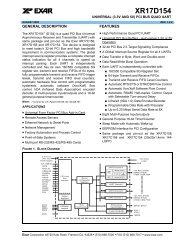
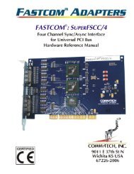
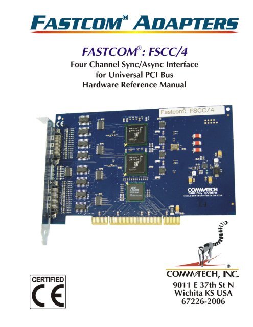
1 Fast<strong>com</strong>: <strong>FSCC</strong>/4<br />
1.1 Features<br />
• High speed synchronous / asynchronous, full duplex, RS-422 / RS-485 ports<br />
• Universal PCI (PCI version 2.3) adapter operates in both 5V and 3.3V PCI slots. This<br />
means the card can work in the high speed PCI-X slots as well as standard PCI slots.<br />
This flexibility allows for a single serial interface board to be used across a wide range of<br />
different types of <strong>com</strong>puters including both current and future <strong>com</strong>puting systems.<br />
• Each port has independent clock generators allowing each to operate at <strong>com</strong>pletely<br />
different baud rates.<br />
• Each port can be operated in True-Asynchronous mode utilizing the onboard FC950<br />
UARTs. When in True-Asynchronous mode, the ports can be operated just like a<br />
standard serial (COM) port. See the True-Asynchronous section for more details.<br />
• Automatic RS-485 handling (e.g. tri-state the driver when idle)<br />
• Receive echo cancel. Disables the line receiver during transmits to prevent receiving the<br />
data that is transmitted in 2-wire 485 modes.<br />
• Transmit and Receive status LEDs for each port.<br />
• On board RS-485 termination network for each receive signal pair<br />
o 100 Ω termination<br />
o 1 kΩ biasing resistors (pull-up and pull-down)<br />
10/11/2012 Fast<strong>com</strong> ® : <strong>FSCC</strong>/4
10<br />
1.2 Board Drawing<br />
1.3 PACKING LIST<br />
• Fast<strong>com</strong>: <strong>FSCC</strong>/4 card<br />
• <strong>FSCC</strong>/4 cable assembly<br />
• Loop back plug<br />
• Fast<strong>com</strong> CD<br />
If an omission has been made, please contact technical support for a replacement.<br />
10/11/2012 Fast<strong>com</strong> ® : <strong>FSCC</strong>/4
11<br />
1.4 Pinouts<br />
We provide access to the two channels of the FASTCOM: <strong>FSCC</strong>/4 through a pair of 0.8mm<br />
CHAMP-50 connectors and two adapter cables (supplied with the board). The adapter cables<br />
consists of a CHAMP-50 male connectors fanning out to two DB25 plugs utilizing high quality<br />
twisted pairs for improved signal performance and noise immunity.<br />
1.4.1 CHAMP-50 (board edge)<br />
10/11/2012 Fast<strong>com</strong> ® : <strong>FSCC</strong>/4
12<br />
1.4.2 DB25 Male (cable)<br />
10/11/2012 Fast<strong>com</strong> ® : <strong>FSCC</strong>/4
13<br />
1.4.3 CHAMP-50 to DB25 Cable Cross-reference<br />
SIGNAL(A) CHAMP50 DB25 Description Direction SIGNAL(B) CHAMP50<br />
GND 1 1 Ground GND 26<br />
TxClkOA- 22 2 Transmit Clock Out - Output TxClkOB- 47<br />
TxDA- 24 3 Transmit Data - Output TxDB- 49<br />
TxClkInA- 20 4 Transmit Click In - Input TxClkInB- 45<br />
RTSA- 14 5 Request To Send - Output RTSB- 39<br />
FST/DTRA- 10 6 Frame Sync Transmit - Output FST/DTRB- 35<br />
DCDA- 4 7 Carrier Detect - Input DCDB- 29<br />
RIA- 12 8 Ring Indicator - Input RIB- 37<br />
CTSA- 2 9 Clear To Send - Input CTSB- 27<br />
DSRA- 6 10 Data Set Ready - Input DSRB- 31<br />
FSRA- 8 11 Frame Sync Receive - Input FSRB- 33<br />
RxDA- 18 12 Receive Data - Input RxDB- 43<br />
RxClkInA- 16 13 Receive Clock In - Input RxClkInB- 41<br />
TxClkOA+ 23 14 Transmit Clock Out + Output TxClkOB+ 48<br />
TxDA+ 25 15 Transmit Data + Output TxDB+ 50<br />
TxClkInA+ 21 16 Transmit Clock In + Input TxClkInB+ 46<br />
RTSA+ 15 17 Request To Send + Output RTSB+ 40<br />
FST/DTRA+ 11 18 Frame Sync Transmit + Output FST/DTRB+ 36<br />
DCDA+ 5 19 Carrier Detect + Input DCDB+ 30<br />
RIA+ 13 20 Ring Indicator + Input RIB+ 38<br />
CTSA+ 3 21 Clear To Send + Input CTSB+ 28<br />
DSRA+ 7 22 Data Set Ready + Input DSRB+ 32<br />
FSRA+ 9 23 Frame Sync Receive + Input FSRB+ 34<br />
RxDA+ 19 24 Receive Data + Input RxDB+ 44<br />
RxClkInA+ 17 25 Receive Clock In + Input RxClkInB+ 42<br />
Table 1: Labled on bracket as Ports 1 and 2<br />
10/11/2012 Fast<strong>com</strong> ® : <strong>FSCC</strong>/4
14<br />
SIGNAL(A) CHAMP50 DB25 Description Direction SIGNAL(B) CHAMP50<br />
GND 1 1 Ground GND 26<br />
TxClkOC- 22 2 Transmit Clock Out - Output TxClkOD- 47<br />
TxDC- 24 3 Transmit Data - Output TxDD- 49<br />
TxClkInC- 20 4 Transmit Click In - Input TxClkInD- 45<br />
RTSC- 14 5 Request To Send - Output RTSD- 39<br />
FST/DTRC- 10 6 Frame Sync Transmit - Output FST/DTRD- 35<br />
DCDC- 4 7 Carrier Detect - Input DCDD- 29<br />
RIC- 12 8 Ring Indicator - Input RID- 37<br />
CTSC- 2 9 Clear To Send - Input CTSD- 27<br />
DSRC- 6 10 Data Set Ready - Input DSRD- 31<br />
FSRC- 8 11 Frame Sync Receive - Input FSRD- 33<br />
RxDC- 18 12 Receive Data - Input RxDD- 43<br />
RxClkInC- 16 13 Receive Clock In - Input RxClkInD- 41<br />
TxClkOC+ 23 14 Transmit Clock Out + Output TxClkOD+ 48<br />
TxDC+ 25 15 Transmit Data + Output TxDD+ 50<br />
TxClkInC+ 21 16 Transmit Clock In + Input TxClkInD+ 46<br />
RTSC+ 15 17 Request To Send + Output RTSD+ 40<br />
FST/DTRC+ 11 18 Frame Sync Transmit + Output FST/DTRD+ 36<br />
DCDC+ 5 19 Carrier Detect + Input DCDD+ 30<br />
RIC+ 13 20 Ring Indicator + Input RID+ 38<br />
CTSC+ 3 21 Clear To Send + Input CTSD+ 28<br />
DSRC+ 7 22 Data Set Ready + Input DSRD+ 32<br />
FSRC+ 9 23 Frame Sync Receive + Input FSRD+ 34<br />
RxDC+ 19 24 Receive Data + Input RxDD+ 44<br />
RxClkInC+ 17 25 Receive Clock In + Input RxClkInD+ 42<br />
Table 2: Labled on bracket as Ports 3 and 4<br />
10/11/2012 Fast<strong>com</strong> ® : <strong>FSCC</strong>/4
15<br />
1.4.4 DB25 Loop back connector<br />
SIGNAL DB25M SIGNAL DB25M<br />
TxClkO+ 14 RxClkI+ 25<br />
TxClkO- 2 RxClkI- 13<br />
TxD+ 15 RxD+ 24<br />
TxD- 3 RxD- 12<br />
RTS+ 17 CTS+ 21<br />
RTS- 5 CTS- 9<br />
FST+ 18 FSR+ 23<br />
FST- 6 FSR- 11<br />
10/11/2012 Fast<strong>com</strong> ® : <strong>FSCC</strong>/4
16<br />
1.5 Installation<br />
1.5.1 Hardware Installation<br />
Important: Static electricity can harm system boards. Perform service at an ESD workstation and<br />
follow proper ESD procedure to reduce the risk of damage to <strong>com</strong>ponents. <strong>Commtech</strong>, Inc.<br />
strongly encourages you to follow proper ESD procedure, which can include wrist straps and<br />
smocks, when handling Fast<strong>com</strong>: <strong>FSCC</strong>/4 boards.<br />
1. Turn off PC power and disconnect the power cord.<br />
2. Remove the PC case cover (if applicable).<br />
3. Unpack the Fast<strong>com</strong>: <strong>FSCC</strong>/4. Keep the box and static bag for warranty repair returns.<br />
4. Select an open PCI slot in your PC (can be either 5V or 3.3V slot).<br />
5. After removing the blank bracket from your PC, install the Fast<strong>com</strong>: <strong>FSCC</strong>/4 in the PC<br />
by pressing it firmly into the slot. Install the bracket screw to hold it firmly in place.<br />
6. Re-install the cover on your PC.<br />
1.5.2 Software Installation (Windows)<br />
Once your card is installed in the <strong>com</strong>puter, you can power on the <strong>com</strong>puter and begin installing<br />
the drivers for the card. Please note that installing this card will actually be installing several<br />
new devices in your system. It will actually install a PCI to PCI bridge device and then it will<br />
appear to install two dual port <strong>FSCC</strong> cards. This is normal. As such steps 1-9 will be repeated<br />
twice: once for each <strong>FSCC</strong> “board” that Windows finds.<br />
1. Windows will detect a new device and start the found new hardware wizard.<br />
2. If it asks to connect to the internet to search for the software, tell it no.<br />
3. The next screen will ask you to automatically search for a driver. Do NOT do this. Select<br />
the option that lets you specify a location to search for the driver.<br />
4. Next it will ask you where to search for the drivers. Put a checkbox next to the option<br />
that lets you specify a location and clear the rest of the boxes.<br />
5. Click the Browse button and browse to where you have the <strong>FSCC</strong> software. If you are<br />
using the Fast<strong>com</strong> CD, that will be the X:\<strong>fast<strong>com</strong></strong>_disks\fscc\YYY folder (where X is<br />
your CD drive and YYY is your version of Windows). If you downloaded the zip file<br />
from our website, you will need to browse to the path that you extracted the zip file.<br />
Again select the folder that corresponds to your version of Windows. Click OK and then<br />
click Next.<br />
6. The next screen may ask you which board type you have and will also show you the path<br />
to the driver that it is about to use. Make sure that path is what you think it should be.<br />
Select the <strong>FSCC</strong> and click Next.<br />
7. The driver will install, you may see a message that warns you that the driver has not been<br />
signed. This is normal and you should continue past this message.<br />
8. The wizard will finish and should report that it successfully installed the <strong>FSCC</strong>.<br />
10/11/2012 Fast<strong>com</strong> ® : <strong>FSCC</strong>/4
17<br />
9. This has installed the driver for the board itself. You will repeat this process three more<br />
times – once for each of the two TrueAsync ports and once for the Sync ports. The steps<br />
will be almost exactly the same as listed above.<br />
1.5.3 Testing the Installation<br />
To fully test the installation of your Fast<strong>com</strong>: <strong>FSCC</strong>/4, you will need a "loop back plug" which<br />
we have included in the box. This loop back plug can be used to test any <strong>FSCC</strong>/4.<br />
These instructions assume that you have already installed the card and have followed the<br />
installation instructions. The Device Manager should show the boards/ports that are installed.<br />
1. Attach supplied DB25 loop back plug to the cable of the port you wish to test<br />
2. Open a <strong>com</strong>mand prompt (Click Start->Run->type “cmd”->click OK) and change to<br />
the directory where you copied the <strong>FSCC</strong> software. The default location is c:\fscc.<br />
3. Change to the examples directory (c:\fscc\examples).<br />
4. Configure the port’s clock:<br />
a. setclock.exe 0 1000000<br />
5. Set the configuration registers:<br />
a. setfeatures.exe 0 0 0 0 0 0<br />
b. fsccset.exe 0 hdlcset.txt<br />
6. Execute the test program:<br />
a. loop.exe 0 0 4094 (press any key to stop the test)<br />
this will test port 0 using data size of up to 4094 bytes.<br />
7. Test and configure the second port:<br />
a. Move the loop back plug to the next port<br />
b. setclock.exe 1 1000000<br />
c. setfeatures.exe 1 0 0 0 0 0<br />
d. fsccset.exe 1 hdlcset.txt<br />
e. loop.exe 1 1 4094 (press any key to stop the test)<br />
8. Test and configure the third port:<br />
a. Move the loop back plug to the next port<br />
b. setclock.exe 2 1000000<br />
c. setfeatures.exe 2 0 0 0 0 0<br />
d. fsccset.exe 2 hdlcset.txt<br />
e. loop.exe 2 2 4094 (press any key to stop the test)<br />
9. Test and configure the fourth port:<br />
10/11/2012 Fast<strong>com</strong> ® : <strong>FSCC</strong>/4
18<br />
a. Move the loop back plug to the next port<br />
b. setclock.exe 3 1000000<br />
c. setfeatures.exe 3 0 0 0 0 0<br />
d. fsccset.exe 3 hdlcset.txt<br />
e. loop.exe 3 3 4094 (press any key to stop the test)<br />
10/11/2012 Fast<strong>com</strong> ® : <strong>FSCC</strong>/4
19<br />
The output will look something like this:<br />
devicename:\\.\<strong>FSCC</strong>0<br />
devicename:\\.\<strong>FSCC</strong>0<br />
tosend :3549<br />
loop: 1 :3549<br />
tosend :5212<br />
loop: 2 :5212<br />
tosend :7398<br />
loop: 3 :7398<br />
tosend :7630<br />
loop: 4 :7630<br />
…<br />
tosend :7888<br />
loop: 1211 :7888<br />
tosend :2130<br />
loop: 1212 :2130<br />
tosend :7203<br />
loop: 1213 :7203<br />
Found 0 errors out of 1213 frames<br />
Wrote 4796745 bytes.<br />
Read 4797958 bytes.<br />
10/11/2012 Fast<strong>com</strong> ® : <strong>FSCC</strong>/4
20<br />
1.6 RS422 / RS485<br />
Most engineers have worked with RS-232 devices at least once in their career. If you have never<br />
worked with RS-422 or RS-485 devices, you will be pleased to know that working with the<br />
FASTCOM: <strong>FSCC</strong>/4 is not much different from working with a standard RS-232 device.<br />
The RS-422 standard was developed to correct some of the deficiencies of RS-232. In<br />
<strong>com</strong>mercial and industrial applications, RS-232 has some significant problems. First, the cable<br />
length between RS-232 devices must be short (usually less than 50 feet at 9600 baud). Second,<br />
many RS-232 errors are the result of cables picking up normal industrial electrical noises such as<br />
fluorescent lights, motors, transformers, and other EMF sources. Third, RS-232 data rates are<br />
functionally limited to 19.2K Baud. On the other hand, the newer RS-422 standard makes cable<br />
lengths up to 5000 feet possible and is highly immune to most industrial noises. Data rates are<br />
also improved -- the FASTCOM: <strong>FSCC</strong>/4 features data rates up to 50 Mbit/sec. These<br />
improvements were made possible by differentially driving and receiving the data as opposed to<br />
the single ended method employed by the RS-232 standard. With the RS-422 standard, the<br />
transmit signal (TX in RS-232) is a differential signal consisting of TX+ and TX-; the receive<br />
signal (RX in RS-232) consists of RX+ and RX-.<br />
Another draw back of RS-232 is that more than two devices cannot share a single cable. This is<br />
also true of RS-422, and that's why the RS-485 standard was developed. RS-485 offers all of the<br />
benefits of RS-422 and also allows multiple units (up to 32) to share the same “twisted pair” of<br />
wires (see diagram on next page). RS-485 is often referred to as a "multi-drop" or "two-wire,<br />
half duplex" network. In order for an RS-485 system to work, only one driver (transmitter) can<br />
occupy the network at a time. This means that each station on the network must control the<br />
enabling/disabling of their drivers in order to avoid network conflicts. If two drivers engage the<br />
network at the same time, data from both will be corrupted. In RS-485 mode, the receivers are<br />
always enabled.<br />
For a more detailed description of RS-422 and RS-485, we re<strong>com</strong>mend the following references:<br />
LINEAR AND INTERFACE CIRCUITS APPLICATIONS, Volume 2: Line Circuits,<br />
Display Drivers. By D.E. Pippenger and E. J. Tobaben. Published 1985 by Texas<br />
Instruments. ISBN-0-89512-185-9<br />
Note: This book may be difficult to find in a bookstore. The best place to get it is<br />
directly from Texas Instruments or from one their <strong>com</strong>ponent dealers. Publication #<br />
SLYA002.<br />
"Driver/Receiver Family Extends Data-Link Performance", ELECTRONIC PRODUCTS,<br />
January 15, 1985. By Dale Pippenger and Joe Miller<br />
10/11/2012 Fast<strong>com</strong> ® : <strong>FSCC</strong>/4
21<br />
1.7 Termination Resistance<br />
In both the RS-422 and the RS-485 mode, the receiver end of the cable between two stations<br />
must be terminated with a resistor equal to the characteristic impedance of the wire. This is to<br />
prevent signal reflections in the wire and to improve noise rejection. However, you do not need<br />
to add a terminator resistor to your cables when you use the Fast<strong>com</strong>: <strong>FSCC</strong>/4. The<br />
termination resistance is built in. We have installed a terminator resistor for each RS422<br />
receiver pair.<br />
If you are using the Fast<strong>com</strong>: <strong>FSCC</strong>/4 in a multi-drop network, the termination resistor should be<br />
removed from all units except the first and last (see the RS-485 illustration below). Call for<br />
technical support if you need to modify the resistor. You may also order the Fast<strong>com</strong>: <strong>FSCC</strong>/4<br />
without the termination resistor installed (it is easier to add the resistor than to remove it).<br />
Observe the resistors in the following drawings and remember that they are built into the<br />
Fast<strong>com</strong>: <strong>FSCC</strong>/4 (shown below):<br />
TX<br />
Typical RS-422 Installation<br />
1 2<br />
RX<br />
R1<br />
R2<br />
TX+<br />
TX-<br />
RX+<br />
RX-<br />
RX+<br />
RX-<br />
TX+<br />
TX-<br />
RX<br />
TX<br />
R1 & R2 - Line Termination (100 ohms)<br />
Typical RS-485 Installation<br />
1<br />
TX<br />
TX+<br />
TX-<br />
R1<br />
R2<br />
RX+<br />
RX-<br />
RX<br />
4<br />
RX<br />
RX+<br />
RX-<br />
TX+<br />
TX-<br />
TX<br />
2<br />
TX<br />
RX<br />
TX+<br />
TX-<br />
RX+<br />
RX-<br />
RX+<br />
RX-<br />
TX+<br />
TX-<br />
RX<br />
TX<br />
3<br />
R1 & R2 - Line Termination (100 ohms)<br />
In addition our termination network also contains a 1kΩ pullup resistor on the + signal and a<br />
1kΩ pull down resistor on the – signal. This ensures that a floating RS485 signal will never<br />
bounce and create spurious data on the receive pins.<br />
10/11/2012 Fast<strong>com</strong> ® : <strong>FSCC</strong>/4
22<br />
1.8 RS-485 Mode<br />
RS-485 is often referred to as a multi-drop or two-wire, half duplex network because the drivers<br />
(transmitters) and receivers share the same two lines. In fact, up to 32 stations can share the<br />
same twisted pair. In order for an RS-485 system to work, only one driver (transmitter) can<br />
occupy the network at a time. This means that each station on the network must control the<br />
enabling/disabling of its drivers in order to avoid network conflicts. If two drivers engage the<br />
network at the same time, data from both will be corrupted. In RS-485 mode, the receivers are<br />
always enabled.<br />
The following cable illustration shows four RS-485 Devices sharing the same twisted pair:<br />
TX+<br />
TX-<br />
TX+<br />
TX+<br />
TX+<br />
TX- TX- TX-<br />
RX+<br />
RX -<br />
RX+ RX + RX +<br />
RX - RX - RX -<br />
1 2 3 4<br />
Note: The termination resistors from Station #2 and Station #3 have been removed.<br />
Not all RS-422 devices feature RS-485 <strong>com</strong>patibility; only RS-485 devices can be connected to<br />
the RS-485 network.<br />
Note that when in the RS-485 mode, you will need to externally connect TX+ to RX+ and TX- to<br />
RX-.<br />
1.9 Difference from Super<strong>FSCC</strong><br />
The Super<strong>FSCC</strong> card features bus-mastering DMA. By utilizing this DMA, the Super is able to<br />
stream gapless, full duplex data at the full 50 Mbits/sec 1 . Where the standard <strong>FSCC</strong> card is only<br />
able to perform the same task at around 20 Mbits/sec. The standard card is capable of operating<br />
at rates up to 50 Mbit/sec with data bursts. It cannot sustain higher rates without generating gaps<br />
in the data (i.e. idle between frames).<br />
1 This is possible as long as the operating parameters are within reason. For instance, you cannot expect to perform<br />
continuous, full duplex operation at 50Mbps with 2 byte frames. This will require reasonable sized frames with a<br />
minimum size of around 1024 bytes. If you have any question about whether the card can meet your needs, please<br />
contact Technical Support.<br />
10/11/2012 Fast<strong>com</strong> ® : <strong>FSCC</strong>/4
23<br />
2 Fast<strong>com</strong> F-Core<br />
2.1 Introduction<br />
• Faced with the inevitability of obsolescence, <strong>Commtech</strong> decided to put an end to the<br />
lifespan problems that plague most <strong>com</strong>puting customers. We designed a serial<br />
<strong>com</strong>munications controller with our customers’ needs in mind, and built a card around it.<br />
• Wholly designed and owned by <strong>Commtech</strong>, Inc, this FPGA based SCC has most of the<br />
features that you are used to seeing in a quality Fast<strong>com</strong> product. It also includes a few<br />
new features that <strong>com</strong>e directly from customer requests.<br />
2.2 Hardware<br />
• Because the F-Core is an FPGA based design, it is easily customizable by <strong>Commtech</strong>’s<br />
engineers to meet the needs of our demanding customers.<br />
• If the existing FPGA technology is ever discontinued or obsoleted by the chip<br />
manufacturer, the design can simply be re-targeted to the next generation of FPGA chip<br />
with no impact on <strong>com</strong>patibility.<br />
2.3 Serial Interface<br />
• Four independent full duplex serial channels<br />
• FIFOs<br />
o Data clocking mechanism independently selectable per channel per direction<br />
• Externally generated Rx and Tx clocks<br />
• Internally generated Rx and Tx clocks<br />
• On chip DPLL clock recovery<br />
• Independent baud rate generators<br />
o RxFIFO = 8KB per port (non-uart modes)<br />
o TxFIFO = 4KB per port (non-uart modes)<br />
o Programmable interrupt trigger levels (watermark)<br />
• Data protocols<br />
o HDLC/SDLC<br />
o Arbitrary maskable sync sequence of up to 4 bytes in length (X-Sync)<br />
o Transparent data without character framing<br />
• Data encoding schemes<br />
o NRZ<br />
o NRZI<br />
o FM0/FM1<br />
10/11/2012 Fast<strong>com</strong> ® : <strong>FSCC</strong>/4
24<br />
o Manchester<br />
o Differential Manchester<br />
• Receive Status Word appended to each <strong>com</strong>plete frame<br />
• Programmable maximum receive frame length checking (RLC = 64 Kbyte)<br />
• Selectable frame sync signals<br />
o Pulse width of one clock at first bit of data<br />
o Pulse width of one clock at last bit of data<br />
o Pulse width of the entire frame<br />
o Optionally insert a variable number of clock cycles between data and FSS<br />
o Selectable polarity<br />
• Optional data flow control using modem control lines (RTS, CTS)<br />
o Option to disable flow control and use signals as general purpose IO<br />
o Selectable polarity<br />
• Programmable 8-bit preamble and postamble with selectable repetition rate (1 to 255<br />
repetitions)<br />
• Data can be oriented as selectable MSB first or LSB first<br />
• Interframe time fill: idle as repetitive 1’s, flags, or sync sequences<br />
• CRC Support<br />
o Automatic handling in the transmit/receive direction<br />
o CRC-CCITT (also known as CRC16-ITU) (HDLC)<br />
o CRC32 (HDLC)<br />
o CRC16<br />
o CRC8 (HDLC)<br />
o Transparent CRC option<br />
o Reset as 0’s / 1’s<br />
• Continuous transmission of 1 to 4096 bytes<br />
• Selectable data rates<br />
o Synchronous (internally clocked) data rates up to 50 Mbit/sec<br />
o Synchronous (externally clocked) data rates up to 30 Mbit/sec<br />
o Asynchronous (DPLL clock recovery) data rates up to 12.5 Mbit/sec<br />
o These maximum data rates are estimates. They are greatly affected by a number<br />
of different factors. See the Baud Rates section for more details.<br />
• Data and clock inversion<br />
10/11/2012 Fast<strong>com</strong> ® : <strong>FSCC</strong>/4
25<br />
• Interruptible hardware timer<br />
• Transmit a single frame on the expiration of the hardware timer<br />
2.4 Data Protocols<br />
• HDLC/SDLC<br />
o Automatic flag detection and transmission<br />
o General frame format: 0x7e,info,CRC,CRC,[CRC,CRC,]0x7e<br />
o Frame format with maskable address enabled:<br />
0x7e,address,[address,]info,CRC,CRC,[CRC,CRC,]0x7e<br />
o Zero insertion/deletion<br />
o One insertion/deletion<br />
o Shared flag mode: opening flag and closing flag of back-to-back frames can use<br />
the same flag.<br />
o Error detection (abort, overrun, underrun, CRC error, too long/short frame)<br />
o Can use CRC8, CRC-CCITT, or CRC32<br />
• Arbitrary Sync Sequence (X-Sync)<br />
o Any begin/end frame sync sequence of up to 4 bytes<br />
o Frame format: SYN1,[SYN2,SYN3,SYN4,]info,[CRC,CRC,<br />
CRC,CRC,][TCR1,TCR2,TCR3,TCR4]<br />
o Maskable: can select all or parts of the sync sequence to be a sync match<br />
o Termination sequence detection up to 4 bytes (maskable)<br />
o Shared flag mode: opening flag and closing flag of back-to-back frames can use<br />
the same flag.<br />
o Error detection<br />
o Can use any of the available CRC methods<br />
• Transparent Mode<br />
o Fully bit transparent (no framing or bit manipulation)<br />
o Can synchronize using selectable frame sync signals<br />
10/11/2012 Fast<strong>com</strong> ® : <strong>FSCC</strong>/4
26<br />
3 Data Flow<br />
3.1 Receive<br />
• In the receive direction, data is clocked into the F-Core’s 8 Kbyte RxFIFO (per channel).<br />
• The RxFIFO is capable of storing up to 512 <strong>com</strong>plete frames of data. The queued frames<br />
can be any size as long as they do not exceed the RxFIFO size. For example, you could<br />
have 512 - 14 byte frames; or you could have 8 - 1022 byte frames; or 16 - 510 byte<br />
frames without overflowing the RxFIFO 1 .<br />
3.1.1 Receive Interrupts 2<br />
3.1.1.1 Receive Frame Start (RFS)<br />
RFS is generated whenever an opening flag, sync sequence or frame sync signal is detected.<br />
3.1.1.2 Receive FIFO Trigger (RFT)<br />
RFT is generated when the number of bytes in the RxFIFO rises above the programmed<br />
RxFIFOTrigger level (e.g. high-water mark).<br />
3.1.1.3 Receive Frame End (RFE)<br />
RFE is generated whenever the RxStatus word for that frame is pushed into the FIFO. When this<br />
occurs, the frame is available to be read from the FIFO.<br />
3.1.1.4 Receive Frame Overflow (RFO)<br />
RFO is generated whenever the maximum number (512) of RxByteCount entries is exceeded.<br />
3.1.1.5 Receive Data Overflow (RDO)<br />
RDO is generated whenever data is received that exceeds the depth (8 Kbyte) of the RxFIFO.<br />
3.1.1.6 Receive Frame Lost (RFL)<br />
RFL is generated whenever the receiver detects an additional frame while an RDO interrupt is<br />
already waiting to be serviced. The RFL bit in the RxStatus word is set for the next message that<br />
is pushed into the RxFIFO. The additional frame is lost.<br />
1 Each frame will have an RxStatus word appended to it in the RxFIFO; the RxStatus word occupies two bytes of<br />
FIFO space. Thus each frame size is actually 2 bytes larger than the actual frame.<br />
2 All bits in the interrupt indication register will reset when the register is read.<br />
10/11/2012 Fast<strong>com</strong> ® : <strong>FSCC</strong>/4
27<br />
3.2 Transmit<br />
• In the transmit direction, data is pushed into the F-Core’s 4 Kbyte TxFIFO (per channel).<br />
• The TxFIFO is capable of storing up to 256 <strong>com</strong>plete frames of data. The queued frames<br />
can be any size as long as they do not exceed the TxFIFO size. For example, you could<br />
have 256 - 16 byte frames; or you could have 4 - 1024 byte frames; or 16 - 256 byte<br />
3.2.1 Transmit Modes<br />
3.2.1.1 Transmit Repeat (XREP)<br />
• When the XREP <strong>com</strong>mand is issued, the F-Core transmits TxByteCount bytes in the<br />
TxFIFO repetitively (treating the repeated block as a single frame) until the transmit reset<br />
(XRES) <strong>com</strong>mand or the SXREP <strong>com</strong>mand is issued.<br />
3.2.1.2 Transmit Frame (XF)<br />
• The XF <strong>com</strong>mand should be considered normal operation of the transmitter.<br />
• When the transmitter is idle and a frame is ready to be sent, the number of bytes in the<br />
frame is entered into TxByteCount and the data (up to 4096 or TxFIFOTrigger bytes at a<br />
time) is pushed into the TxFIFO. When the XF <strong>com</strong>mand is issued, the transmitter<br />
be<strong>com</strong>es active and the number of bytes in TxByteCount is pushed out of the TxFIFO<br />
into the transmitter.<br />
• The XF <strong>com</strong>mand is issued with each queued frame, but is only acted upon by the<br />
controller if the transmitter is in the idle state.<br />
3.2.1.3 Transmit on Timer (TXT)<br />
The F-Core has the ability to transmit one queued frame on the expiration of the hardware timer<br />
(see 4.12) repetitively. When the timer expires (TIN interrupt), the transmitter sends one<br />
<strong>com</strong>plete frame from the TxFIFO. When the frame is <strong>com</strong>pletely sent, it returns to an idle state<br />
until the next timer expiration. The user is able to send a single frame repetitively using the<br />
XREP <strong>com</strong>mand. Also, the user is able to queue frames up to the TxFIFO depth or a maximum<br />
of 256 frames, using the normal XF <strong>com</strong>mand. Data is only transmitted on timer expiration<br />
boundaries. If the user queues a frame, it is not transmitted until the next timer expiration. If the<br />
TxFIFO is empty when the timer expires then no action is taken.<br />
3.2.1.4 Transmit on External Signal (TEXT)<br />
The F-Core has the ability to transmit one queued frame on the transition of an external signal,<br />
repetitively. When the transition is detected, the transmitter sends one <strong>com</strong>plete frame from the<br />
TxFIFO. When the frame is <strong>com</strong>pletely sent, it returns to an idle state until the next transition is<br />
detected. The user is able to send a single frame repetitively using the XREP <strong>com</strong>mand. Also,<br />
the user is able to queue frames up to the TxFIFO depth or a maximum of 256 frames, using the<br />
normal XF <strong>com</strong>mand. Data is only transmitted on a detected transition on the external signal. If<br />
the user queues a frame, it is not transmitted until the next transition. If the TxFIFO is empty<br />
when the transition occurs then no action is taken.<br />
10/11/2012 Fast<strong>com</strong> ® : <strong>FSCC</strong>/4
28<br />
3.2.2 Transmit Interrupts<br />
3.2.2.1 Transmit FIFO Trigger 3 (TFT)<br />
The TFT interrupt is used to indicate that the TxFIFO is ready to accept more data. It is<br />
generated when:<br />
• The number of bytes in the TxFIFO falls below the programmed TxFIFOTrigger level<br />
(low-water mark)<br />
• When moving from idle to active, if the BytesInTxFIFO count is less than the<br />
TxFIFOTrigger level anytime the XF <strong>com</strong>mand is issued<br />
3.2.2.2 All Sent (ALLS)<br />
The ALLS interrupt is generated any time the transmitter moves from an active to an idle state.<br />
This is an indication that it has finished transmitting data.<br />
3.2.2.3 Transmit Data Underrun (TDU)<br />
The TDU interrupt is generated whenever transmitter moves from an active to an idle state, and<br />
the number of bytes pushed into the TxFIFO has not yet reached the current TxByteCount. This<br />
is an indication that the software is not moving data fast enough.<br />
3 There will be some level of hysteresis (TBD) in the Tx trigger level to provide time for the bus interface to fill the<br />
FIFO without retriggering the interrupt due to outgoing bytes.<br />
10/11/2012 Fast<strong>com</strong> ® : <strong>FSCC</strong>/4
29<br />
4 Global Features Details<br />
4.1 Clocking System<br />
There are several different ways to clock data into and out of the F-Core. There can be<br />
externally sourced clocks in both transmit and receive directions. The transmit clock can be<br />
derived from our onboard clock source. The receive clock can be recovered from the received<br />
data using DPLL. Also the receive clock can be used as the transmit clock.<br />
In the transmit direction, the data is considered valid on the rising edge of the effective transmit<br />
clock. The receive data is considered valid on the falling edge of the effective receive clock. As<br />
an option, we are able to flip the clock edges that correspond to valid data.<br />
The effective transmit clock is always outputted on the TxClkOut pin, whether it is derived on<br />
board clock generator, from the RxClk, or from a signal on the TxClkIn pins.<br />
If you select an external clock mode, please make sure the clock is present before trying to<br />
operate the ports. If a clock is not present, and an operation is performed on the port that<br />
causes something in the Command Register to execute, it may cause the F-Core to appear to lock<br />
up and cause an error. This is because the <strong>com</strong>mands execute using the transmit or receive<br />
clock and with no clock the <strong>com</strong>mand cannot <strong>com</strong>plete.<br />
4.1.1 Onboard Clock Generators<br />
Each port has a fully independent, software settable clock generator that feeds the baud rate<br />
generator of the FCore. Each clock generator can be set to nearly any frequency between 20kHz<br />
and 200MHz. This clock is fed into the internal baud rate generator of the FCore where it is<br />
divided down to get the desired baud rate. In the following section, any clock mode that runs off<br />
of the internal BGR is utilizing this onboard clock generator.<br />
The drivers for each OS contain a function or program that accepts the desired frequency and a<br />
parts per million (ppm) variable as inputs. Sometimes the clock generator cannot be set to<br />
exactly the desired frequency, in this case you utilize the ppm variable to allow for some amount<br />
of deviation in the calculation and the algorithm uses the frequency that is closest to the desired<br />
input but within the specified ppm.<br />
10/11/2012 Fast<strong>com</strong> ® : <strong>FSCC</strong>/4
30<br />
4.1.2 Clock Modes<br />
Table 3: Clock Modes of the F-Core<br />
Clock<br />
Mode<br />
Receive Source<br />
Transmit Source<br />
External<br />
(RxClk)<br />
Internal BGR<br />
DPLL<br />
External<br />
(TxClkIn)<br />
Internal BGR<br />
Effective<br />
RxClk<br />
0 • •<br />
1 • •<br />
2 • •<br />
3 • •<br />
4 • • 1<br />
5 • •<br />
6 • •<br />
7 • •<br />
Note 1- In DPLL Mode TxClkOut = BGR / 16<br />
Note 2: Clock source to BGR is always the onboard clock input to the FPGA<br />
Note 3: Clock source to DPLL is always the BGR<br />
4.1.2.1 Clock Mode 0<br />
Separate, externally generated (off board) receive and transmit clocks are supplied to the F-Core<br />
via their respective pins (RxClk and TxClkIn).<br />
4.1.2.2 Clock Mode 1<br />
Receive clock is supplied directly from the RxClk pins. Transmit clock is derived from the<br />
internal BGR fed by the onboard clock generator.<br />
4.1.2.3 Clock Mode 2<br />
Both receive and transmit clocks are externally sourced from the RxClk pin.<br />
4.1.2.4 Clock Mode 3<br />
Receive clock <strong>com</strong>es from the DPLL clock recovery. The BGR is fed by the onboard clock<br />
generator and it delivers a reference clock of a frequency equal to 16 times the nominal bit rate<br />
for the DPLL which in turn generates the receive clock. Transmit clock <strong>com</strong>es directly from the<br />
TxClkIn pin.<br />
4.1.2.5 Clock Mode 4<br />
Receive clock <strong>com</strong>es from the DPLL clock recovery. The BGR is fed by the onboard clock<br />
generator and it delivers a reference clock of a frequency equal to 16 times the nominal bit rate<br />
for the DPLL which in turn generates the receive clock. Transmit clock is derived from the<br />
internal BGR / 16.<br />
10/11/2012 Fast<strong>com</strong> ® : <strong>FSCC</strong>/4
31<br />
4.1.2.6 Clock Mode 5<br />
Receive clock <strong>com</strong>es from the DPLL clock recovery. The BGR is fed by the onboard clock<br />
generator and it delivers a reference clock of a frequency equal to 16 times the nominal bit rate<br />
for the DPLL which in turn generates the receive clock. The generated receive clock is used as<br />
the transmit clock as well.<br />
4.1.2.7 Clock Mode 6<br />
Receive clock is derived from the internal BGR fed by the onboard clock generator. Transmit<br />
clock is supplied directly from the TxClkIn pins.<br />
4.1.2.8 Clock Mode 7<br />
Both the receive and transmit clocks are derived from the internal BGR fed by the onboard clock<br />
generator.<br />
Note: this mode should only be used with the receiver disabled.<br />
10/11/2012 Fast<strong>com</strong> ® : <strong>FSCC</strong>/4
32<br />
4.1.3 Baud Rates<br />
Because this is an interrupt driven board, there are some limitations as to the speeds that you can<br />
expect. Our testing indicates that you will be able to maintain continuous (gapless), 20 Mbit/sec<br />
baud rates full duplex (that is simultaneous transmit and receive) on a single channel. This will<br />
generate more interrupts than is reasonable for a conventional CPU to handle. The exact<br />
maximum will vary with each system’s configuration.<br />
The length and quality of the cables connecting to the other device is also a contributing factor to<br />
maximum baud rates. Longer cable lengths and lower quality cable will decrease the achievable<br />
data rates.<br />
Improper line termination will attenuate the signal and can also decrease the maximum data<br />
rates.<br />
The exact speed that you can achieve will also depend on your system’s ability to move the data<br />
fast enough. This means the size of your data frames - it is easier for the system to write fewer<br />
larger frames than it is to write many smaller frames.<br />
4.1.4 Clock Recovery (DPLL)<br />
The F-Core offers the advantage of recovering the received clock from the received data by<br />
means of internal DPLL circuitry, thus eliminating the need to transfer additional clock<br />
information via a separate serial clock line. For this purpose, the DPLL is supplied with a<br />
‘reference clock’ from the BGR, which is 16 times the expected data clock rate (clock modes 3,<br />
4 and 5). The transmit clock may be obtained externally (clock mode 3), by dividing the output<br />
of the BGR by a constant factor of 16 (clock mode 4) or also directly from the DPLL (clock<br />
mode 5).<br />
The main task of the DPLL is to derive a receive clock and to adjust its phase to the in<strong>com</strong>ing<br />
data stream in order to enable optimal bit sampling.<br />
The method for clock recovery depends on the selected data encoding.<br />
The following functions are implemented:<br />
4.1.4.1 Interference Rejection and Spike Filtering<br />
Two or more edges in the same directional data stream within a time period of 16 reference<br />
clocks are considered to be interference and consequently no additional clock adjustment is<br />
performed.<br />
4.1.4.2 Phase Adjustment (PA)<br />
Referring to Figure 1, Figure 2, and Figure 3, in the case where an edge appears in the data<br />
stream within the PA fields of the time windows, the phase is adjusted by 1/16 of the data.<br />
4.1.4.3 Phase Shift (PS) (NRZ & NRZI only)<br />
Referring to Figure 1 in the case where an edge appears in the data stream within the PS field of<br />
the time window, a second sampling of the bit is forced and the phase is shifted by 180 degrees.<br />
Note: Edges in all other parts of the time windows are ignored.<br />
10/11/2012 Fast<strong>com</strong> ® : <strong>FSCC</strong>/4
33<br />
This operation facilitates a fast and reliable synchronization for most <strong>com</strong>mon applications.<br />
Above all, it implies a very fast synchronization because of the phase shift feature: one edge on<br />
the received data stream is enough for the DPLL to synchronize, thereby eliminating the need for<br />
synchronization patterns, sometimes called preambles. However, in case of extremely high jitter<br />
of the in<strong>com</strong>ing data stream the reliability of the clock recovery cannot be guaranteed.<br />
The F-Core offers the option to disable the Phase Shift function for NRZ and NRZI encodings.<br />
In this case, the PA fields are extended as shown in Figure 2.<br />
Now, the DPLL is more insensitive to high jitter amplitudes but needs more time to reach the<br />
optimal sampling position. To ensure correct data sampling, preambles should precede the data<br />
information.<br />
Figure 1, Figure 2 and Figure 3 explain the DPLL algorithms used for the different data<br />
encodings.<br />
Figure 1 - DPLL Algorithm for NRZ and NRZI Coding with Phase Shift Enabled<br />
10/11/2012 Fast<strong>com</strong> ® : <strong>FSCC</strong>/4
34<br />
Figure 2 - DPLL Algorithm for NRZ and NRZI Coding with Phase Shift Disabled<br />
Figure 3 - DPLL Algorithm for FM0, FM1 and Manchester Coding<br />
4.1.4.4 DPLL Status Flag<br />
To supervise correct function an RxStatus flag in the status register (6.2.7) reflects the DPLL’s<br />
synchronous/asynchronous state. When synchronized, if the DPLL detects an edge in the data<br />
that is more than 1/16 of the data clock away from center, it enters an asynchronous state, set the<br />
DPLLA status flag, and attempt to resynchronize. If the loss of synchronization occurs while<br />
receiving a frame that frame is aborted, marked <strong>com</strong>plete and reception restarts on the next begin<br />
frame condition with a synchronized DPLL.<br />
Note that it is possible for the DPLLA bit/status to not be telling the whole truth. With all<br />
revisions of firmware the DPLLA status is only updated when an edge occurs and the clock<br />
phase is out of the window (as described in the manual). As a result, a long sequence of no edges<br />
does not give a DPLLA indication until the next edge occurs.<br />
10/11/2012 Fast<strong>com</strong> ® : <strong>FSCC</strong>/4
35<br />
4.1.4.5 DPLL Reset<br />
The DPLL is forced into a reset mode if more than 32 (default setting) receive clocks elapse<br />
without an edge in the data. Practically this allows for proper operation and will lock on to<br />
gapped frames with no edges between them. The implementation inserts an extra bit at the<br />
beginning of any given frame sequence (either an extra zero or one depending on the relative<br />
phase of the free running internal receive clock and the first edge in the data) that follows one of<br />
these no edge periods. This should not present any problems for HDLC modes, or any mode that<br />
uses a synchronization sequence (X-Sync, or FSR gated receive) and will only cause difficulty in<br />
Transparent mode when no beginning sync is used. It is not re<strong>com</strong>mended to use configure<br />
continuous receive, in transparent mode, using the DPLL, with long sequences of 1′s or 0′s with<br />
NRZ line encoding.<br />
The number of clock edges before the DPLL is considered out of sync is now configurable in a<br />
register (0×58) the DPLL RESET register. It may have a value from 1 to 511 and is the number<br />
of clocks without an edge that the DPLL considers OK, more clocks than this and it will snap to<br />
the next edge (with the possibility of the extra bit being clocked in as described above). The<br />
number set is in 8 clock increments, so a value of 1 is 8 clocks, 2 16 clocks, etc. The default<br />
value is 4, which yields 32 clocks as described above.<br />
10/11/2012 Fast<strong>com</strong> ® : <strong>FSCC</strong>/4
36<br />
4.2 Data Encoding<br />
The F-Core supports the following coding schemes for serial data:<br />
• Non-Return-To-Zero (NRZ)<br />
• Non-Return-To-Zero-Inverted (NRZI)<br />
• FM0 (also known as Bi-Phase Space)<br />
• FM1 (also known as Bi-Phase Mark)<br />
• Manchester (also known as Bi-Phase)<br />
• Differential Manchester<br />
4.2.1 NRZ and NRZI Encoding<br />
• NRZ: The signal level corresponds to the value of the data bit. By setting the data<br />
inversion bit, the SCC may invert the transmission and reception of data.<br />
• NRZI: A logical ‘0’ is indicated by a transition and a logical ‘1’ is indicated by no<br />
transition at the beginning of the bit cell.<br />
Clk<br />
NRZ<br />
NRZI<br />
Value 0 1 1 0 0 1 0<br />
Figure 4 - NRZ and NRZI encoding<br />
4.2.2 FM0 and FM1 Encoding<br />
• FM0: An edge occurs at the beginning of every bit cell. A logical ‘0’ has an additional<br />
edge in the center of the bit cell, whereas a logical ‘1’ has none. The transmit clock<br />
precedes the receive clock by 90°.<br />
• FM1: An edge occurs at the beginning of every bit cell. A logical ‘1’ has an additional<br />
edge in the center of the bit cell; a logical ‘0’ has none. The transmit clock precedes the<br />
receive clock by 90°.<br />
TxClk<br />
RxClk<br />
FM0<br />
FM1<br />
Value 1 1 0 0 1 0<br />
Figure 5 - FM0 and FM1 encoding<br />
10/11/2012 Fast<strong>com</strong> ® : <strong>FSCC</strong>/4
37<br />
4.2.3 Manchester Encoding<br />
• Manchester: In the first half of the bit cell, the physical signal level corresponds to the<br />
logical value of the data bit. At the center of the bit cell this level is inverted. The<br />
transmit clock precedes the receive clock by 90°. The bit cell is shifted by 180° in<br />
<strong>com</strong>parison with FM coding.<br />
• The normal mode of operation would be considered the G.E. Thomas version of<br />
Manchester. You can effectively switch to the IEEE 802.3 version of Manchester by<br />
setting bit CCR1:TDP = 1.<br />
TxClk<br />
RxClk<br />
Manchester<br />
Value 1 1 0 0 1 0<br />
Figure 6 - Manchester encoding<br />
4.2.4 Differential Manchester Encoding 1<br />
Also known as CDP, Conditional DePhase encoding, is a method of encoding data in which data<br />
and clock signals are <strong>com</strong>bined to form a single self-synchronizing data stream. It is a<br />
differential encoding, using the presence or absence of transitions to indicate logical value. This<br />
gives it several advantages over vanilla Manchester encoding:<br />
• Detecting transitions is often less error-prone than <strong>com</strong>paring against a threshold in a<br />
noisy environment.<br />
• Because only the presence of a transition is important, polarity is not. Differential<br />
schemes work exactly the same if the signal is inverted (wires swapped). (Other line<br />
codes with this property include NRZI, bipolar encoding, and MLT-3 encoding).<br />
A '1' bit is indicated by making the first half of the signal equal to the last half of the previous<br />
bit's signal i.e. no transition at the start of the bit-time. A '0' bit is indicated by making the first<br />
half of the signal opposite to the last half of the previous bit's signal i.e. a zero bit is indicated by<br />
a transition at the beginning of the bit-time. In the middle of the bit-time there is always a<br />
transition, whether from high to low, or low to high. A reversed scheme is possible, and no<br />
advantage is given by using either scheme.<br />
Differential Manchester is specified in the IEEE 802.5 standard for token ring LANs, and is used<br />
for many other applications, including magnetic and optical storage.<br />
Note: In differential Manchester encoding, if a "1" is represented by one transition, then a "0" is<br />
represented by two transitions and vice versa.<br />
1 Customer request. From Wikipedia: http://en.wikipedia.org/wiki/Differential_Manchester_encoding<br />
10/11/2012 Fast<strong>com</strong> ® : <strong>FSCC</strong>/4
38<br />
4.3 Receive Status Word<br />
The contents of the receive status word consists of the lower 16-bits of the status register (6.2.7).<br />
At the detection of a frame end condition, the current state of the status register is pushed onto<br />
the RxFIFO as the last word of each stored frame and appears in your data with the lower order<br />
byte first. In this way, the RxStatus word describes the state of the F-Core at the time the frame<br />
ended.<br />
Note: this causes your expected frame size to increase by two bytes.<br />
4.4 Receive Length Check<br />
When enabled, this programmable 16-bit value is <strong>com</strong>pared to the total number of bytes received<br />
for the current frame. The RLC terminates an in<strong>com</strong>ing frame when “bytes received” is greater<br />
than the programmed RLC count (CCR2:RLC). “Bytes received” increments for each byte that<br />
<strong>com</strong>es into the receiver. This includes any sync, address, data, crc or term bytes that may be<br />
enabled. It counts everything.<br />
When the receive length condition is reached a message end condition is generated (including the<br />
receive status word) , the bytes are transferred to the RxFIFO and the RLEX bit in the status<br />
register (6.2.7) is set. The received data is transferred to the host where it shall be dealt with<br />
appropriately.<br />
This function has a quirk that must be explained so that you can get exactly the numbers that you<br />
need for your data. If you leave CRC checking enabled, the firmware considers the last byte(s)<br />
received to be the CRC value even if it is only data. As such if you do not set the bit DRCRC<br />
(which turns off CRC checking in the receiver) you will lose the last byte(s) of your data because<br />
it thought they were CRC. In order to accurately pass all of your data over to the receive FIFO<br />
you need to set bit CCR1:DRCRC = 1.<br />
Example: Receive the data portion of a frame that has 2 sync bytes and 1028 bytes of data, no<br />
CRC and no termination:<br />
Set RLC = 1029, SYNC2F=0, DRCRC=1<br />
Read size = 1030 = (1028 byte frame + 2 RxStatus bytes)<br />
Note: Maximum RLC = 65535 bytes<br />
4.5 Frame Sync Signals<br />
In some cases a given system may require the use of frame synchronization signals (FSR and<br />
FST) to enable reception of data. These optional signals facilitate <strong>com</strong>munication with such a<br />
system. The F-Core automatically generates these frame sync signals in relation to its transmit<br />
data. It also automatically utilizes these signals to synchronize with receive data. There are<br />
three operating modes of the frame sync signals.<br />
• Mode 1: The sync signal <strong>com</strong>pletely frames the data<br />
o In the transmit direction, the Frame Sync Transmit (FST) signal will be active<br />
sometime before the clock edge (less than one clock period) that corresponds with<br />
the first data bit. FST will go inactive sometime after the clock edge (less than<br />
one clock period) corresponding to the last data bit.<br />
10/11/2012 Fast<strong>com</strong> ® : <strong>FSCC</strong>/4
39<br />
o In the receive direction, the receiver must begin clocking in data on the first clock<br />
edge with an active Frame Sync Receive (FSR) signal and proceed with the frame<br />
start sequence. The receiver will stop clocking in data on the first clock edge with<br />
an inactive frame sync signal and mark the received data block as a <strong>com</strong>plete<br />
frame with the end sequence.<br />
o In this mode, the FSR signal will only be used to synchronize data when in<br />
Transparent Mode.<br />
• Mode 2: The sync signal is found at the beginning of data<br />
o In the transmit direction, the FST signal will go active sometime before the clock<br />
edge (less than one clock period) that corresponds with the first data bit. FST will<br />
then go inactive sometime (less than one clock period) after that same clock edge.<br />
o In the receive direction, the receiver must begin clocking in data on the first clock<br />
edge with an active FSR signal and proceed with the frame start sequence. The<br />
receiver will continue clocking in data until a frame end condition is reached.<br />
The receiver will ignore the active FSR signal if its duration spans more than one<br />
clock edge; i.e. the FSR signal only enables the receiver when the receiver is in an<br />
idle state.<br />
o In this mode, the FSR signal will only be used to synchronize data when in<br />
Transparent Mode. This signal will both begin the next receive data block and<br />
end the previous data block.<br />
• Mode 3: The sync signal is found at the end of data<br />
o In the transmit direction, the FST signal will go active sometime before the clock<br />
edge (less than one clock period) that corresponds with the last data bit. FST will<br />
then go inactive sometime (less than one clock period) after that same clock edge.<br />
o In the receive direction, the receiver must stop clocking in data on the first clock<br />
edge with an inactive FSR signal and proceed with the frame end sequence. The<br />
receiver will ignore the inactive FSR signal if its duration spans more than one<br />
clock edge; i.e. the FSR signal only disables the receiver when the receiver is in<br />
an active state.<br />
o In this mode, the FSR signal could be used to terminate a receive data block when<br />
in Transparent Mode as well as X-Sync mode. This signal will both terminate the<br />
current receive data block and begin the next data block when using Transparent<br />
Mode.<br />
• Mode 4: Both Mode2 and Mode 3 at the same time<br />
• Mode 5: Frame sync Mode 5 is similar to mode 1, except there are independent controls<br />
for both the leading and trailing edge of the FST signal. When mode 5 is enabled<br />
CCR2[7:4] control the leading edge of the FST signal and CCR2[11:8] control the<br />
trailing edge. CCR2[11:8] will have no effect in any other Frame Sync Mode.<br />
The user can optionally choose to insert a number of clock cycles between data and FSS. The 4-<br />
bit value, CCR2:FSTO & CCR2:FSRO, specifies the number of additional transmit or receive<br />
10/11/2012 Fast<strong>com</strong> ® : <strong>FSCC</strong>/4
40<br />
clocks cycles to shift the frame sync signals with a range of –8 clocks to +7 clocks. The diagram<br />
shown below is with FSTO set to the default of 0 inserted clocks.<br />
CLK0<br />
Sync1<br />
Data1<br />
Idle<br />
Valid Region<br />
Active<br />
Valid Data<br />
Sync2<br />
Data2<br />
Sync3<br />
Data3<br />
Figure 7 - Frame Sync Modes<br />
4.6 Modem Control Signals<br />
The F-Core provides two pins (RTS and CTS) per serial channel to facilitate transmission<br />
control. There are also several modem control signals from the True-Async mode for each<br />
channel. When not using the True-Async mode, these pins are free to use as general purpose<br />
I/O’s.<br />
• The input pins each create a maskable interrupt upon state change<br />
• The current state of the input pins is accessible via the Status Register<br />
• The current state of the input pins is inserted into the RxStatus word for each frame<br />
4.6.1 Request to send (RTS)<br />
• In automatic mode, the RTS pin goes active as soon as data is ready to be transmitted.<br />
This implies that the RTS signal will go active at least 1 clock prior to data being<br />
transmitted, and goes inactive 1 clock after data transmission is <strong>com</strong>plete. If data is ready<br />
to be transmitted, but has not actually been transmitted yet (i.e. because CTS is inactive),<br />
RTS must remain active to facilitate RTS-CTS handshaking.<br />
• Selectable polarity. User can select whether the signal is active low or active high<br />
(default: active low).<br />
• Can be used as a general purpose output pin<br />
4.6.2 Clear to send (CTS)<br />
• The transmitter is paused if the CTS input signal is inactive and enabled if active.<br />
• The current byte is <strong>com</strong>pletely sent even if CTS be<strong>com</strong>es inactive during transmission.<br />
o In HDLC mode, the current frame is aborted with the HDLC abort sequence<br />
(seven contiguous ‘1’ bits). The transmitter returns to the idle state.<br />
10/11/2012 Fast<strong>com</strong> ® : <strong>FSCC</strong>/4
41<br />
o In X-Sync mode, the current frame will be closed using the termination sequence<br />
or sync signal (if in use). The transmitter returns to the idle state.<br />
o A CTS Abort (CTSA) interrupt will be generated after CTS deassertion causes an<br />
abort sequence to be transmitted. If CTS deassertion does not occur during<br />
transmission of a frame, this interrupt will not be generated.<br />
• Selectable polarity. User can select whether the signal is active low or active high<br />
(default: active low).<br />
• Can be used as a general-purpose input pin<br />
4.6.3 DTR<br />
This shall be a general-purpose output pin. This signal will be present from our True-Async.<br />
module, so we will connect it to the SCC as well.<br />
4.6.4 DSR, CD, RI<br />
These signals shall be general-purpose input pins. These signals will be present from our True-<br />
Async module, so we will connect them to the SCC as well.<br />
4.7 Preambles and Postambles<br />
There shall be an optional 8-bit preamble and an optional 8-bit postamble. When enabled, each<br />
shall have a selectable repetition rate of between 1 and 255 repetitions. These can be used to aid<br />
in the synchronization of a clock recovery circuit or in the enabling of an RS485 driver or<br />
receiver.<br />
4.8 Order of Bit Transmission<br />
Usually, data bytes within element fields shall be transmitted least significant bit first (i.e. the<br />
first bit of the sequence number that is transmitted shall have the weight 2 0 ). However, as an<br />
option, the order of transmission can be reversed so that bytes shall be transmitted most<br />
significant bit first (i.e. the first bit of the sequence number that is transmitted shall have the<br />
weight 2 7 ).<br />
If CRC transmission is enabled, the CRC bytes shall always be transmitted to the line<br />
<strong>com</strong>mencing with the coefficient of the highest term (i.e. MSB first), regardless of the order of<br />
bit transmission.<br />
4.9 Interframe Time Fill<br />
Inter-frame time fill shall be ac<strong>com</strong>plished by repetitively transmitting contiguous flags, sync<br />
sequences or eight contiguous "1" bits. Selection of the inter-frame time fill method depends on<br />
systems requirements.<br />
Note: The receiver must be able to ignore back-to-back SYNC until there is SYNC that is<br />
followed by non-SYNC data. At that instance, the receiver will no longer look for SYNC<br />
characters and will clock in raw data until a stop condition is reached. If you have SYNC2F set,<br />
the hardware consider the last SYNC sequence before the non-SYNC sequence to be the "real"<br />
SYNC and just put the SYNC sequence into the FIFO once. All the rest of them would be idles<br />
and are not valid data. If SYNC2F is not set, the hardware strips only the "real" SYNC and will<br />
10/11/2012 Fast<strong>com</strong> ® : <strong>FSCC</strong>/4
42<br />
no longer be hunting for SYNC characters anymore. If one should happen to appear in the data,<br />
nothing will happen (unless it also matches the TERM character)<br />
4.10 CRC Frame Checking Sequences<br />
The CRC frame checking sequence is calculated for the entire length of the frame, excluding the<br />
opening and or closing sequences, the CRC, and any bits inserted for transparency. The<br />
calculation shall begin immediately after the opening (SYNC) sequence and continue, over the<br />
designated portion of the entire frame and end at the closing (TERM) sequence. If the CRC<br />
calculation/<strong>com</strong>parison for a given frame does not match, the CRC bit in the STAR register will<br />
be set.<br />
4.10.1 8-bit frame checking sequence (CRC-8)<br />
Per the HDLC specification, the 8-bit CRC shall be the ones <strong>com</strong>plement of the sum (modulo 2)<br />
of<br />
a) the remainder of<br />
x k (x 7 + x 6 + x 5 + x 4 + x 3 + x 2 + x + 1)<br />
divided (modulo 2) by the generator polynomial<br />
x 8 + x 2 + x + 1,<br />
where k is the number of bits in the frame existing between, but not including, the final bit of the<br />
opening flag and the first bit of the CRC, excluding start and stop elements (start/stop<br />
transmission), and bits (synchronous transmission) and octets (start/stop transmission) inserted<br />
for transparency, and<br />
b) The remainder of the division (modulo 2) by the generator polynomial<br />
x 8 + x 2 + x + 1<br />
of the product of x 8 by the content of the frame existing between, but not including, the<br />
final bit of the opening flag and the first bit of the CRC, excluding start and stop elements<br />
(start/stop transmission), and bits (synchronous transmission) and octets (start/stop<br />
transmission) inserted for transparency.<br />
As a typical implementation, at the transmitter, the initial content of the register of the device<br />
<strong>com</strong>puting the remainder of the division is preset to all ones and is then modified by division by<br />
the generator polynomial (as described above) of the address, control and information fields; the<br />
ones <strong>com</strong>plement of the resulting remainder is transmitted as the 8-bit CRC.<br />
At the receiver, the initial content of the register of the device <strong>com</strong>puting the remainder is preset<br />
to all ones. The final remainder after multiplication by x 8 and then division (modulo 2) by the<br />
generator polynomial<br />
x 8 + x 2 + x + 1<br />
of the serial in<strong>com</strong>ing protected bits and the CRC, will be “1111 0011” (x 7 through x 0 ,<br />
respectively) in the absence of transmission errors.<br />
10/11/2012 Fast<strong>com</strong> ® : <strong>FSCC</strong>/4
43<br />
4.10.2 16-Bit frame checking sequence<br />
4.10.2.1 CRC-CCITT<br />
Per the HDLC specification, the 16-bit CRC shall be the ones <strong>com</strong>plement of the sum (modulo<br />
2) of<br />
a) The remainder of<br />
x k ( x 15 + x 14 + x 13 + x 12 + x 11 + x 10 + x 9 + x 8 + x 7 + x 6 + x 5 + x 4 + x 3 + x 2 + x + 1)<br />
divided (modulo 2) by the generator polynomial<br />
x 16 + x 12 + x 5 + 1,<br />
where k is the number of bits being protected by the CRC and<br />
b) The remainder of the division (modulo 2) by the generator polynomial<br />
x 16 + x 12 + x 5 + 1,<br />
of the product of x 16 by the content of the k bits being protected.<br />
As a typical implementation, at the transmitter, the initial content of the register of the device<br />
<strong>com</strong>puting the remainder of the division is preset to all ones and is then modified by division by<br />
the generator polynomial (as described above) of the address, control and any remaining bits of<br />
the designated k bits being protected; the ones <strong>com</strong>plement of the resulting remainder is<br />
transmitted as the 16-bit CRC.<br />
At the receiver, the initial content of the register of the device <strong>com</strong>puting the remainder is preset<br />
to all ones. The final remainder after multiplication by x16 and then division (modulo 2) by the<br />
generator polynomial<br />
x 16 + x 12 + x 5 + 1,<br />
of the serial in<strong>com</strong>ing protected bits and the CRC will be 0001 1101 0000 1111 (x 15 through x 0 ,<br />
respectively) in the absence of transmission errors.<br />
4.10.2.2 CRC-16<br />
CRC-16 is not specified in the HDLC document but <strong>com</strong>monly used as a frame checking<br />
sequence for non-HDLC devices, therefore it will be available to users for non-HDLC modes.<br />
Commonly referred to as IBM’s CRC-16, this algorithm uses the following polynomial:<br />
x 16 +x 15 + x 2 + 1<br />
4.10.3 32-bit frame checking sequence (CRC-32)<br />
Per the HDLC specification, the 32-bit CRC shall be the ones <strong>com</strong>plement of the sum (modulo<br />
2) of<br />
a) the remainder of<br />
x k (x 31 + x 30 + x 29 + x 28 + x 27 + x 26 + x 25 + x 24 + x 23 + x 22 + x 21 + x 20 + x 19 + x 18 + x 17 +<br />
x 16 + x 15 + x 14 + x 13 + x 12 + x 11 + x 10 + x 9 + x 8 + x 7 + x 6 + x 5 + x 4 + x 3 + x 2 + x + 1)<br />
divided (modulo 2) by the generator polynomial<br />
x 32 + x 26 + x 23 + x 22 + x 16 + x 12 + x 11 + x 10 + x 8 + x 7 + x 5 + x 4 + x 2 + x + 1,<br />
10/11/2012 Fast<strong>com</strong> ® : <strong>FSCC</strong>/4
44<br />
where k is the number of bits being protected by the CRC and<br />
b) The remainder of the division (modulo 2) by the generator polynomial<br />
x 32 + x 26 + x 23 + x 22 + x 16 + x 12 + x 11 + x 10 + x 8 + x 7 + x 5 + x 4 + x 2 + x + 1<br />
of the product of x 32 by the content of the k bits being protected.<br />
As a typical implementation, at the transmitter, the initial content of the register of the device<br />
<strong>com</strong>puting the remainder of the division is preset to all ones and is then modified by division by<br />
the generator polynomial (as described above) of the address, control and any remaining bits of<br />
the designated k bits being protected; the ones <strong>com</strong>plement of the resulting remainder is<br />
transmitted as the 32-bit CRC.<br />
At the receiver, the initial content of the register of the device <strong>com</strong>puting the remainder is preset<br />
to all ones. The final remainder after multiplication by x 32 and then division (modulo 2) by the<br />
generator polynomial<br />
x 32 + x 26 + x 23 + x 22 + x 16 + x 12 + x 11 + x 10 + x 8 + x 7 + x 5 + x 4 + x 2 + x + 1,<br />
of the serial in<strong>com</strong>ing protected bits and the CRC will be 1100 0111 0000 0100 1101 1101 0111<br />
1011 (x 31 through x 0 , respectively) in the absence of transmission errors.<br />
4.11 Data and Clock Inversion<br />
• With this option selected, data will be received/transmitted inverted on a per bit basis.<br />
This includes all data fields, flags and idle sequences. This inversion should take place as<br />
the data stream enters or leaves the F-Core. See CCR1:RDP and CCR1:TDP<br />
• With this option selected, receive and transmit clocks will be inverted before entering or<br />
leaving the F-Core, effectively changing the part from a falling edge device to a rising<br />
edge device when enabled. See CCR1: TCOP, CCR1:TCIP and CCR1:RCP<br />
4.12 Hardware Timer<br />
The hardware timer is a configurable countdown timer. The timer can be clocked by any one of<br />
three sources: effective TxClk, effective RxClk, PCI clock. It can optionally count down once<br />
and then stop or to reset and count down continuously. The Timer register is 32-bits: three of<br />
them are used as control signals leaving a 29-bit count down value. When the timer expires it<br />
triggers a TIN interrupt.<br />
4.13 Transmit on Timer<br />
The <strong>FSCC</strong> will have the ability to transmit one queued frame on the expiration of the hardware<br />
timer repetitively. When the timer expires (TIN interrupt), the transmitter will send one<br />
<strong>com</strong>plete frame from the TxFIFO. When the frame is <strong>com</strong>pletely sent, it will return to an idle<br />
state until the next timer expiration. The user will be able to send a single frame repetitively<br />
using the XREP <strong>com</strong>mand. Also, the user will be able to queue frames up to the TxFIFO depth<br />
or a maximum of 256 frames, using the normal XF <strong>com</strong>mand. Data is only transmitted on timer<br />
expiration boundaries. If the user queues a frame, it is not transmitted until the next timer<br />
expiration. If the TxFIFO is empty when the timer expires then no action is taken.<br />
10/11/2012 Fast<strong>com</strong> ® : <strong>FSCC</strong>/4
45<br />
4.14 Zero Bit Insertion<br />
The transmitter shall examine the frame content between the two sync sequences including the<br />
address and CRC fields, when present, and shall insert a "0" bit after all sequences of 5<br />
contiguous "1" bits (including the last 5 bits of the CRC) to ensure that a flag sequence is not<br />
simulated. The receiver shall examine the frame content and shall discard any "0" bit which<br />
directly follows 5 contiguous "1" bits. This is the standard HDLC bit stuffing mechanism<br />
4.15 One Bit Insertion<br />
Similar to the zero bit insertion (bit stuffing) mechanism, as defined by the HDLC protocol, the<br />
F-Core offers a <strong>com</strong>pletely new feature of inserting/deleting a ’one’ after seven consecutive<br />
‘zeros’ into the transmit/receive data stream. This method is useful if clock recovery is<br />
performed by DPLL.<br />
If using NRZ data encoding there are possibly long sequences without edges in the receive data<br />
stream in case of successive ‘0’s received, and the DPLL may lose synchronization.<br />
By enabling the one bit insertion feature it is guaranteed that at least after<br />
– 5 consecutive ‘1’s a ‘0’ will appear (bit stuffing), and after<br />
– 7 consecutive ‘0’s a ‘1’ will appear (one insertion)<br />
and thus a correct function of the DPLL is ensured.<br />
Note: As with the bit stuffing, the ‘one insertion’ is fully transparent to the user, but it is not in<br />
accordance with the HDLC protocol, i.e. it can only be applied in proprietary systems using<br />
circuits that also implement this function, such as the SAB 82532/PEB 20534.<br />
10/11/2012 Fast<strong>com</strong> ® : <strong>FSCC</strong>/4
46<br />
5 Detailed Protocol Description<br />
5.1 HDLC/SDLC<br />
In HDLC, all transmissions are in frames. The frame format structure does not include bits<br />
inserted for transparency.<br />
5.1.1 General Frame Format<br />
Each frame consists of the following fields (left to right transmission sequence, hexadecimal<br />
values):<br />
Flag 7E<br />
Addr-H<br />
1 byte<br />
Addr-L<br />
1 byte<br />
Info<br />
n bytes<br />
Frame Checking Sequence<br />
CRC8 CRC-CCITT CRC32<br />
1 byte 2 bytes 4 bytes<br />
Flag 7E<br />
Where:<br />
Flag = Flag sequence<br />
Addr-H = Station address field high byte<br />
Addr-L = Station address field low byte<br />
Info = Info field<br />
CRC8 = 8-bit frame checking sequence byte<br />
CRC-CCITT = 16-bit frame checking sequence word<br />
CRC32 = 32-bit frame checking sequence dword<br />
5.1.2 Elements of the Frame<br />
5.1.2.1 Flag Sequence<br />
All frames start and end with the flag sequence (0x7E). All data stations that are attached to the<br />
data link shall continuously hunt for this sequence. Thus, the flag is used for frame<br />
synchronization. A single flag may be used as both the closing flag for one frame and the<br />
opening flag for the next frame if the next frame immediately follows the previous frame<br />
without any idle line time (i.e., back-to-back).<br />
5.1.2.2 Address Fields<br />
The address field or fields immediately follow the opening flag and identify the station for which<br />
the <strong>com</strong>mand is intended. When more than one address field is used, they shall be present in the<br />
frame in a consecutive manner. If enabled, the receiver will scan for the appropriate 8 or 16-bit<br />
maskable address. If the address of the in<strong>com</strong>ing frame does not match the address of the<br />
receiver, then the frame is rejected and the hunt for flag sequence is re-initiated. 8-bit addresses<br />
will use the Addr-H byte and the Addr-L byte will be ignored.<br />
The Address High/Low bytes can be masked on a per bit basis by setting the corresponding bits<br />
in the mask register. This allows extended broadcast address recognition. Masked bit positions<br />
always match in <strong>com</strong>parison of the received frame address with the respective address fields.<br />
This feature is applicable to all HDLC protocol modes with address recognition. It is disabled if<br />
all bits of mask register are set to ‘zero’.<br />
10/11/2012 Fast<strong>com</strong> ® : <strong>FSCC</strong>/4
47<br />
As an option the 8/16 bit address field of received frames can be pushed to the receive data<br />
buffer (first one/two bytes of the frame).<br />
5.1.2.2.1 All-Station Address<br />
The address field bit pattern 11111111 is defined as the all-station address. The all-station<br />
address may be used for all-station polling. When there is more than one receiving data station<br />
for which a <strong>com</strong>mand with the all-station is intended, any responses from these data stations<br />
shall not interfere with one another. If the 16 bit address scheme is in use, we will be <strong>com</strong>paring<br />
the first octet and ignoring the second octet.<br />
5.1.2.2.2 No-Station Address<br />
The bit pattern 00000000 in the first octet of the extended or non-extended address field is<br />
defined as the no-station address. The no-station address shall never be assigned to a data<br />
station. The no-station address may be used for testing when it is intended that no data station<br />
react or respond to a frame containing the no-station address. If the 16 bit address scheme is in<br />
use, we will be <strong>com</strong>paring the first octet and ignoring the second octet.<br />
5.1.2.2.3 Group Address<br />
The group address register is a second 16-bit maskable address <strong>com</strong>parison register that can be<br />
used to define custom group addresses. For example, in certain usages of HDLC, the address<br />
0xFC or 0xFE can be used to address all stations in a group. This register is <strong>com</strong>pared in<br />
addition to the primary address register. If the address <strong>com</strong>parison matches either of the<br />
registers, the frame will be received.<br />
5.1.2.3 Info Field<br />
Info field may be any sequence of 8-bit bytes of up to a maximum of MAXFRAMESIZE bytes.<br />
Note: The data between the start and end flags must be byte aligned (8-bits long). For example,<br />
5 bit data bytes are not allowed.<br />
Note: MAXFRAMESIZE is 65535-2 if RLC is enabled, or 2^32 (effectively infinite) if RLC is<br />
disabled. Any sync, term, CRC or address bytes that are to be transferred to the FIFO will also<br />
have to be accounted for.<br />
5.1.2.4 CRC Fields<br />
Three frame checking sequences are specified; an 8-bit frame checking sequence (CRC8), a 16-<br />
bit frame checking sequence (CRC-CCITT), and a 32-bit frame checking sequence (CRC32).<br />
The 16-bit frame checking sequence is normally used. The 8-bit frame checking sequence is for<br />
use by prior agreement in those cases where short frames are used such that the protection<br />
afforded is adequate and/or the overhead of a longer frame checking sequence is of concern. The<br />
32-bit frame checking sequence is for use by prior agreement in those cases that need a higher<br />
degree of protection than can be provided by the 16-bit frame checking sequence.<br />
5.1.3 Data Reception<br />
In HDLC mode, data will begin to be moved into the RxFIFO immediately following detection<br />
of the opening flag (0x7E). Optionally, if Address checking is enabled, the first byte or bytes of<br />
data will be checked against the selected station address. If the station address matches,<br />
10/11/2012 Fast<strong>com</strong> ® : <strong>FSCC</strong>/4
48<br />
reception of data is continued. If the station address does not match, the received data is<br />
discarded and the receiver is returned to the non-synchronized, IDLE state.<br />
Once synchronization is achieved, data will continue to be clocked in until one of the defined<br />
stop conditions is detected:<br />
• The closing flag (0x7E) is detected<br />
• The Receiver Reset <strong>com</strong>mand is issued<br />
• The programmed Receive Length Check (RLC) has been reached<br />
• An abort sequence is detected (seven contiguous ‘1’ bits)<br />
After any of the above stop conditions have been met:<br />
• The receiver is to return to the non-synchronized (IDLE) state in which it is hunting for<br />
the opening flag.<br />
• Reception of data is internally disabled until synchronization is regained.<br />
• The current receive data block is to be marked as closed.<br />
o If CRC is enabled, the calculated CRC will be checked against appropriate CRC<br />
byte(s)<br />
o The RxStatus word will be appended to the data<br />
5.1.4 Data Transmission<br />
In HDLC mode, when data moved out of the TxFIFO and into the transmitter, the frame is<br />
assembled before being clocked out. The opening flag is prepended to the outbound data. The<br />
selected CRC algorithm will be run on the data as it moves through the transmitter. The final<br />
calculated CRC bytes are inserted into the appropriate field. Likewise, on its way through the<br />
transmitter, the data is parsed for places that need zero bit insertion (including the CRC bytes).<br />
Upon <strong>com</strong>pletion the closing flag is added and the data is clocked out.<br />
• Optionally the CTS signal can be used to control data transmission.<br />
• After <strong>com</strong>pleting data transmission, the selected Interframe time fill is automatically sent.<br />
5.1.5 Shared Flag Mode<br />
A single flag may be used as both the closing flag for one frame and the opening flag for the next<br />
frame if the next frame immediately follows the previous frame without any idle line time (i.e.,<br />
back-to-back). The shared flag will act as a terminating sequence on the current frame and the<br />
opening sequence on the subsequent frame.<br />
5.1.6 Invalid Frame<br />
An invalid frame is defined as one that is not properly bounded by two flags or one that is too<br />
short (that is, shorter than 16 bits between flags when using the 8-bit CRC, shorter than 24 bits<br />
between flags when using the 16-bit CRC, and shorter than 40 bits between flags when using the<br />
32-bit CRC). The hardware will mark the invalid frame as closed and will reset the VFR bit in<br />
the RxStatus word. The invalid frame will then be passed on to the RxFIFO and will be handled<br />
by software.<br />
10/11/2012 Fast<strong>com</strong> ® : <strong>FSCC</strong>/4
49<br />
5.1.7 Aborted Frame<br />
During reception of a frame, if there is ever detected seven or more contiguous ‘1’ bits, this shall<br />
be considered an abort <strong>com</strong>mand. If an abort <strong>com</strong>mand is detected, the hardware will set the<br />
ABF bit in the status register (6.2.7). The aborted frame will then be passed on to the RxFIFO<br />
and will be handled by software.<br />
10/11/2012 Fast<strong>com</strong> ® : <strong>FSCC</strong>/4
50<br />
5.2 Character Oriented Synchronous (X-Sync) Mode<br />
Character oriented protocols achieve synchronization between transmitting and receiving stations<br />
by means of special SYNC sequences.<br />
5.2.1 General Frame Format<br />
Each frame consists of the following fields (left to right transmission sequence, hexadecimal<br />
values):<br />
X-Sync Sequence<br />
Frame Checking Sequence<br />
Terminating Sequence<br />
SYNC1<br />
SYNC2<br />
SYNC3<br />
SYNC4<br />
Info<br />
n bytes<br />
CRC8<br />
CRC-CCITT<br />
or CRC16<br />
CRC32<br />
TERM1<br />
TERM2<br />
TERM3<br />
TERM4<br />
1 byte 1 byte 1 byte 1 byte 1 byte 2 bytes 4 bytes 1 byte 1 byte 1 byte 1 byte<br />
Where:<br />
SYNC1 = First sync byte<br />
SYNC2 = Optional second sync byte<br />
SYNC3 = Optional third sync byte<br />
SYNC4 = Optional fourth sync byte<br />
Info = N-byte data field<br />
CRC8 = 8-bit frame checking sequence byte<br />
CRC-CCITT = 16-bit frame checking sequence word<br />
CRC16 = 16-bit frame checking sequence word<br />
CRC32 = 32-bit frame checking sequence dword<br />
TERM1 = Optional first termination byte<br />
TERM2 = Optional second termination byte<br />
TERM3 = Optional third termination byte<br />
TERM4 = Optional fourth termination byte<br />
5.2.2 Elements of the Frame<br />
5.2.2.1 X-Sync Sequence<br />
The SYNC sequence can be one, two, three or four bytes long. Each bit of the SYNC sequence<br />
is maskable, meaning it can match anything, allowing you to receive frames with differing<br />
SYNC sequences.<br />
5.2.2.2 Info Field<br />
Info field may be any sequence of bits of up to MAXFRAMESIZE bytes.<br />
Note: The data between the SYNC and TERM flags must be byte aligned (8-bits long). For<br />
example, 5 bit data bytes are not allowed.<br />
Note: MAXFRAMESIZE is 65535-2 if RLC is enabled, or 2^32 (effectively infinite) if RLC is<br />
disabled. Any sync, term, CRC or address bytes that are to be transferred to the FIFO will also<br />
have to be accounted for.<br />
10/11/2012 Fast<strong>com</strong> ® : <strong>FSCC</strong>/4
51<br />
5.2.2.3 CRC Fields<br />
Four frame checking sequences are specified: an 8-bit frame checking sequence (CRC8); two 16-<br />
bit frame checking sequences (CRC-CCITT and CRC-16); and a 32-bit frame checking sequence<br />
(CRC32). The CRC-16 frame checking sequence is normally used. The 8-bit frame checking<br />
sequence is for use by prior agreement in those cases where short frames are used such that the<br />
protection afforded is adequate and/or the overhead of a longer frame checking sequence is of<br />
concern. The 32-bit frame checking sequence is for use by prior agreement in those cases that<br />
need a higher degree of protection than can be provided by the 16-bit frame checking sequence.<br />
5.2.2.4 Termination Sequence<br />
The programmed termination sequence can also be selected as one, two, three, four bytes or<br />
entirely disabled. Each bit of the TERM sequence is maskable, meaning it can match anything,<br />
allowing it to match multiple sequences.<br />
5.2.3 Data Reception<br />
In X-Sync mode, data will begin to be moved into the RxFIFO immediately following detection<br />
of the entire SYNC sequence (with the option of pushing the SYNC sequence itself into the<br />
RxFIFO).<br />
Once synchronization is achieved, data will continue to be clocked in until one of the defined<br />
stop conditions is detected:<br />
• The programmed termination sequence is detected<br />
• The Receiver Reset <strong>com</strong>mand is issued<br />
• There is a pulse on the Frame Sync Receive (FSR) signal (Mode 3)<br />
• The programmed Receive Length Check (RLC) has been reached<br />
• The HUNT <strong>com</strong>mand is issued<br />
After any of the above stop conditions have been met:<br />
• The receiver is to return to the non-synchronized, IDLE state in which it is hunting for<br />
the SYNC sequence.<br />
• Reception of data is internally disabled until synchronization is regained.<br />
• The current receive data block is to be marked as closed.<br />
o If CRC is enabled, the appropriate CRC byte(s) will be checked<br />
o The RxStatus word will be appended to the data<br />
5.2.4 Data Transmission<br />
• User data transmitted in X-Sync mode will be sent out following the programmed SYNC<br />
sequence.<br />
• If enabled, the internally calculated CRC value is appended to the message frame. 1<br />
• Optionally the CTS signal can be used to control data transmission.<br />
1 Internally generated SYN characters are always excluded from CRC calculations<br />
10/11/2012 Fast<strong>com</strong> ® : <strong>FSCC</strong>/4
52<br />
• If TERM sequence is enabled, the transmitter can automatically append the chosen<br />
TERM sequence. Optionally the TERM sequence can be left off.<br />
• After <strong>com</strong>pleting data transmission, the selected Interframe time fill is automatically sent.<br />
5.2.5 Shared Flag Mode<br />
In X-Sync, this option allows the terminating sequence of the current frame to be used as the<br />
sync sequence of the next frame as long as that next frame immediately follows the current frame<br />
without any idle line time (i.e., back-to-back). The shared flag will act as the closing sequence<br />
for the current frame and the opening sequence for the subsequent frame.<br />
10/11/2012 Fast<strong>com</strong> ® : <strong>FSCC</strong>/4
53<br />
5.3 Transparent Mode<br />
In transparent mode, fully transparent data transmission and reception without any framing is<br />
performed (i.e. no flag or sync detection). This allows user-defined protocols to be used.<br />
5.3.1 Data Reception<br />
In the base transparent configuration, the receiver will be constantly enabled and will push<br />
everything that is on the line into the RxFIFO. There will be no frame delimiters in the data to<br />
mark the end of a frame. RxByteCount will count all bytes that enter into the RxFIFO and if its<br />
value reaches its maximum, it will simply reset and continue counting.<br />
There are two ways to trigger a non-error end of frame condition. That would be with the<br />
Receive Length Check or the Frame Sync Receive signal.<br />
Note: A frame end condition will still occur at the specified error conditions.<br />
If enabled, the Receive Length Check can be used to signal an end of frame condition. The<br />
RxStatus word will be appended on to the received data.<br />
If frame synchronization is enabled using the Frame Sync Receive (FSR) signal, reception of<br />
data will be enabled and/or disabled at the appropriate clock edges. In this case, the<br />
RxByteCount will equal the number of bytes received while data reception was enabled and the<br />
RxStatus word will be appended to the end of the received data.<br />
5.3.2 Data Transmission<br />
The transmitter will shift the data in the TxFIFO directly to the output. The transmitted data will<br />
be <strong>com</strong>pletely unmodified. When the transmitter is in an idle state, it will output either a<br />
continuous stream of 1’s or a repeating byte as defined by the lower 8 bits of the SSR. If you<br />
want to output the SSR byte, you must set CCR0:ITF=1.<br />
If frame synchronization is enabled, the generated Frame Sync Transmit (FST) signal will reflect<br />
the first and last bit of the transmitted data.<br />
10/11/2012 Fast<strong>com</strong> ® : <strong>FSCC</strong>/4
54<br />
5.4 True-Asynchronous Mode<br />
Each port can be operated in True-Asynchronous mode utilizing the two on board FC950<br />
UARTS. When the driver is switched to True-Asynchronous mode, the ports can be operated<br />
just like a standard serial (COM or tty) port. This will disable the synchronous <strong>FSCC</strong> interface<br />
and transfer board control over to the given COM or tty port. See FCR to enable this mode.<br />
5.4.1 Features<br />
• Baud rates up to 15 Mbps in normal mode<br />
• Single full-duplex asynchronous channel<br />
• 128-byte deep transmitter / receiver FIFO<br />
• Fully software <strong>com</strong>patible with industry standard 16C550 type UARTs<br />
• Flexible clock prescaler from 1 to 31.875<br />
• 9-bit data framing as well as 5,6,7 and 8<br />
• Detection of bad data in the receiver FIFO<br />
• Transmitter and receiver can be disabled<br />
• Programmable special character detection<br />
• Arbitrary trigger levels for receiver and transmitter FIFO interrupts and automatic inband<br />
and out-ofband flow control<br />
• Automatic handling of RS485 (i.e. the line driver tri-states when idle)<br />
• Receive echo cancel. Disables the line receiver during transmits to prevent receiving the<br />
data that is transmitted in 2-wire 485 modes.<br />
10/11/2012 Fast<strong>com</strong> ® : <strong>FSCC</strong>/4
55<br />
6 Register Description<br />
6.1 Base Address Registers<br />
Table 4 – Base Address Registers descriptions<br />
Name Address Size Description Page<br />
BAR0 0x000 – 0x054 256 Bytes F-Core Port A 55<br />
0x080 – 0x0D4 F-Core Port B 55<br />
BAR1 0x000 – 0x007 128 Bytes FC950 Port A 88<br />
0x008 – 0x00F FC950 Port B 88<br />
BAR2 0x000 – 0x07F 128 Bytes Board Control 95<br />
6.2 F-Core Registers<br />
Table 5 – F-Core Register Descriptions<br />
Address Access Type Register Page<br />
Port A Port B Name Description<br />
0x00 0x80 W TxFIFO Transmit FIFO 56<br />
R RxFIFO Receive FIFO 56<br />
0x04 0x84 W TxByteCount Transmit Byte Count FIFO 56<br />
R RxByteCount Receive Byte Count FIFO 56<br />
0x08 0x88 R/W FIFO Trigger Transmit and Receive FIFO Trigger Level 56<br />
0x0C 0x8C R FIFO Byte Count Number of bytes in the FIFOs 57<br />
0x10 0x90 R FIFO Frame Count Number of queued frames in the FIFOs 58<br />
0x14 0x94 W CMDR Command Register 59<br />
0x18 0x98 R STAR Status Register 61<br />
0x1C 0x9C R/W CCR0 Channel Configuration Register 0 65<br />
0x20 0xA0 R/W CCR1 Channel Configuration Register 1 69<br />
0x24 0xA4 R/W CCR2 Channel Configuration Register 2 73<br />
0x28 0xA8 R/W BGR Baud-rate Generator Register 75<br />
0x2C 0xAC R/W SSR Synchronization Sequence Register 76<br />
0x30 0xB0 R/W SMR Synchronization Mask Register 77<br />
0x34 0xB4 R/W TSR Termination Sequence Register 78<br />
0x38 0xB8 R/W TMR Termination Mask Register 79<br />
0x3c 0xBC R/W RAR Receive Address Register 80<br />
0x40 0xC0 R/W RAMR Receive Address Mask Register 81<br />
0x44 0xC4 R/W PPR Preamble & Postamble Register 82<br />
0x48 0xC8 R/W TCR Timer Control Register 83<br />
0x4c 0xCC R VSTR Version Status Register 84<br />
0x50 0xD0 R ISR Interrupt Status Register 85<br />
0x54 0xD4 R/W IMR Interrupt Mask Register 87<br />
0x58 0xD8 R/W DPLLR DPLL Reset ontrol Register 89<br />
10/11/2012 Fast<strong>com</strong> ® : <strong>FSCC</strong>/4
56<br />
6.2.1 FIFO locations (0x00/0x80)<br />
Writing data to the TxFIFO is done with 32-bit dword writes to this address space.<br />
Reading data from the RxFIFO is done with 32-bit dword reads from this address space.<br />
6.2.2 Byte Count FIFO locations (0x04/0x84)<br />
The TxByteCount FIFO is the total number of data bytes in the corresponding frame in the<br />
TxFIFO. This count will be written here after the data has been written into the TxFIFO.<br />
The RxByteCount FIFO is the total number of data bytes in the corresponding frame plus<br />
the RxStatus word plus any other bytes that have been pushed to the FIFO. This number is<br />
the total number of bytes actually written to the RxFIFO. This count will be written after<br />
the frame has been <strong>com</strong>pleted.<br />
6.2.3 FIFO Trigger Levels (0x08/0x88)<br />
31 30 29 28 27 26 25 24 23 22 21 20 19 18 17 16<br />
0 0 0 0<br />
TXTRG11<br />
TXTRG10<br />
TXTRG9<br />
TXTRG8<br />
TXTRG7<br />
TXTRG6<br />
TXTRG5<br />
TXTRG4<br />
TXTRG3<br />
TXTRG2<br />
TXTRG1<br />
TXTRG0<br />
15 14 13 12 11 10 9 8 7 6 5 4 3 2 1 0<br />
0 0 0<br />
RXTRG12<br />
RXTRG11<br />
RXTRG10<br />
RXTRG9<br />
RXTRG8<br />
RXTRG7<br />
RXTRG6<br />
RXTRG5<br />
RXTRG4<br />
RXTRG3<br />
RXTRG2<br />
RXTRG1<br />
RXTRG0<br />
TXTRG[11:0] – Transmit FIFO Trigger Level<br />
A 12-bit value written to this location sets the TxFIFO trigger level from 0x004 (four) to<br />
0xFFC (4092) bytes . The TxFIFO trigger level generates a TFT interrupt whenever the<br />
data level in the transmit FIFO falls below this preset trigger level.<br />
RXTRG[12:0] – Receive FIFO Trigger Level<br />
A 13-bit value written to this location sets the RxFIFO trigger level from 0x04 (four) to<br />
0x1FFC (8188) bytes. The RxFIFO trigger level generates an interrupt whenever the<br />
receive FIFO rises above this preset trigger level.<br />
Note: In terms of efficiency, it is best to set the FIFO levels to DWORD aligned values (i.e.<br />
divisible by 4) because all bus transfers happen as DWORDs, so setting a non-DWORD value<br />
does not gain anything.<br />
10/11/2012 Fast<strong>com</strong> ® : <strong>FSCC</strong>/4
57<br />
6.2.4 FIFO Byte Count (0x0C/0x8C)<br />
31 30 29 28 27 26 25 24 23 22 21 20 19 18 17 16<br />
0 0 0<br />
TXCNT12<br />
TXCNT11<br />
TXCNT10<br />
TXCNT9<br />
TXCNT8<br />
TXCNT7<br />
TXCNT6<br />
TXCNT5<br />
TXCNT4<br />
TXCNT3<br />
TXCNT2<br />
TXCNT1<br />
TXCNT0<br />
15 14 13 12 11 10 9 8 7 6 5 4 3 2 1 0<br />
0 0<br />
RXCNT13<br />
RXCNT12<br />
RXCNT11<br />
RXCNT10<br />
RXCNT9<br />
RXCNT8<br />
RXCNT7<br />
RXCNT6<br />
RXCNT5<br />
RXCNT4<br />
RXCNT3<br />
RXCNT2<br />
RXCNT1<br />
RXCNT0<br />
TXCNT[12:0] – Transmit FIFO Level Counter<br />
When read, this 13-bit value will return the total number of bytes currently in the transmit<br />
FIFO from 0x00 (zero) to 0x1000 (4096) bytes.<br />
RXCNT[13:0] – Receive FIFO Level Counter<br />
When read, this 14-bit value will return the total number of bytes currently in the receive<br />
FIFO from 0x00 (zero) to 0x2000 (8192) bytes.<br />
10/11/2012 Fast<strong>com</strong> ® : <strong>FSCC</strong>/4
58<br />
6.2.5 FIFO Frame Count (0x10/0x90)<br />
31 30 29 28 27 26 25 24 23 22 21 20 19 18 17 16<br />
0 0 0 0 0 0 0<br />
TFCNT8<br />
TFCNT7<br />
TFCNT6<br />
TFCNT5<br />
TFCNT4<br />
TFCNT3<br />
TFCNT2<br />
TFCNT1<br />
TFCNT0<br />
15 14 13 12 11 10 9 8 7 6 5 4 3 2 1 0<br />
0 0 0 0 0 0<br />
RFCNT9<br />
RFCNT8<br />
RFCNT7<br />
RFCNT6<br />
RFCNT5<br />
RFCNT4<br />
RFCNT3<br />
RFCNT2<br />
RFCNT1<br />
RFCNT0<br />
TFCNT[8:0] – Transmit FIFO Frame Count<br />
When read, this 9-bit value returns the number of <strong>com</strong>plete frames that are queued in the<br />
TxFIFO from 0x00 (zero) to 0x100 (256). This is essentially the number of entries in the<br />
TxByteCount FIFO.<br />
RFCNT[9:0] – Receive FIFO Frame Count<br />
When read, this 10-bit value returns the number of <strong>com</strong>plete frames that are queued in the<br />
RxFIFO from 0x00 (zero) to 0x200 (512). This is essentially the number of entries in the<br />
RxByteCount FIFO.<br />
10/11/2012 Fast<strong>com</strong> ® : <strong>FSCC</strong>/4
59<br />
6.2.6 CMDR – Command Register (0x14/0x94)<br />
Transmit Commands<br />
Receive Commands<br />
31 30 29 28 27 26 25 24 23 22 21 20 19 18 17 16<br />
0 0<br />
TXEXT<br />
TXT<br />
TRES<br />
SXREP<br />
XREP<br />
XF<br />
0 0 0 0 0 0<br />
RRES<br />
HUNT<br />
General Commands<br />
15 14 13 12 11 10 9 8 7 6 5 4 3 2 1 0<br />
0 0 0 0 0 0 0 0 0 0 0 0 0 0<br />
STIMR<br />
TIMR<br />
Note 4: All bits of the <strong>com</strong>mand register are self-clearing. All <strong>com</strong>mand bits are executed at detection of a<br />
logic level ‘1’.<br />
TIMR – Start Timer Command<br />
This <strong>com</strong>mand starts the hardware timer. Whenever the timer expires, a TIMR interrupt<br />
is generated.<br />
STIMR – Stop Timer Command<br />
This <strong>com</strong>mand stops the hardware timer. When executed, the timer will immediately<br />
terminate operation and will reset back to its initial state.<br />
HUNT – Enter HUNT State Command<br />
This <strong>com</strong>mand forces the receiver to enter its HUNT state immediately. Thus<br />
synchronization is released and the receiver begins searching for new SYNC sequences.<br />
RRES – Receiver Reset Command<br />
The receive FIFO is cleared and the receiver is reset to its initial state. The receive FIFO<br />
accepts new receive data immediately after receiver reset has <strong>com</strong>pleted.<br />
XF – Transmit Frame<br />
After having written data to the TxFIFO, this <strong>com</strong>mand initiates the transmission of the<br />
frame. The appropriate opening sequence is automatically added to the data by the F-<br />
Core. See the Transmit Data Flow section 3.2 for more details.<br />
XREP – Transmit Repeatedly<br />
Operates the same as XF <strong>com</strong>mand, except that this <strong>com</strong>mand will transmit the given<br />
data repeatedly until stopped. See the Transmit Data Flow section 3.2 for more details.<br />
SXREP – Stop Transmitting Repeatedly<br />
This <strong>com</strong>mand signals the transmitter to stop sending the repeated frame at the end of the<br />
current frame.<br />
10/11/2012 Fast<strong>com</strong> ® : <strong>FSCC</strong>/4
60<br />
TRES – Transmitter Reset<br />
When executed, the controller will immediately stop transmitting the current frame and<br />
switch to the IDLE sequence. The transmit FIFO is cleared of any data and the<br />
transmitter is reset to its initial state. The transmit FIFO accepts new transmit data<br />
immediately after transmitter reset has <strong>com</strong>pleted.<br />
TXT – Transmit on Timer<br />
Use in conjunction with the XF or XREP <strong>com</strong>mands to transmit a single, <strong>com</strong>plete frame<br />
on the expiration of the timer. For example, if you wanted to transmit a single frame<br />
repeatedly on the expiration of the timer, you would send both the TXT and the XREP<br />
<strong>com</strong>mand at the same time.<br />
See section 3.2.1.3 for more details on transmit on timer.<br />
TXEXT – Transmit on External Signal<br />
Use in conjunction with the XF <strong>com</strong>mand to transmit a single, <strong>com</strong>plete frame on the<br />
transition of an external signal (CTS, DSR, RI, CD) as chosen via CCR0:EXTSEL.<br />
Similar in operation to the TXT <strong>com</strong>mand, this uses a transition on an external signal to<br />
trigger a single frame send.<br />
See section 3.2.1.4 for more details on transmit on external signal.<br />
10/11/2012 Fast<strong>com</strong> ® : <strong>FSCC</strong>/4
61<br />
6.2.7 STAR – Status Register (0x18/0x98)<br />
Controller Status<br />
31 30 29 28 27 26 25 24 23 22 21 20 19 18 17 16<br />
0 0 0 0 0 0 0<br />
TDO<br />
0<br />
TXEA<br />
TXTA<br />
XREPA<br />
DPLLA<br />
CE<br />
TBC<br />
TFE<br />
Receive Status Word<br />
FIFO Status Frame Status Input Pin Status<br />
15 14 13 12 11 10 9 8 7 6 5 4 3 2 1 0<br />
0 0<br />
RDO<br />
RFL<br />
VFR<br />
RLEX<br />
CRC<br />
ABF<br />
0 0 0 0<br />
RI<br />
CD<br />
DSR<br />
CTS<br />
Note 1: Bit 24 will be reset upon a read of the status register. Bits 13 through 8 will be reset upon the pushing<br />
of the RxStatus word into the RxFIFO. Bits 21 through 16 will not reset and will always correspond to the<br />
current state of those conditions. The last four bits will not reset and will always correspond to the present<br />
state of the input pins.<br />
Note 2: The Receive Status Word will show up as the last two bytes of your data. It is read least significant<br />
byte first. So the last two bytes of your data will read 0x0802 for a CRC error and an active RI signal<br />
CTS – Clear To Send<br />
Reflects the current state of the CTS input pin. Does not reset.<br />
DSR – Data Set Ready<br />
Reflects the current state of the DSR input pin. Does not reset.<br />
CD – Carrier Detect<br />
Reflects the current state of the CD input pin. Does not reset.<br />
RI – Ring Indicator<br />
Reflects the current state of the RI input pin. Does not reset.<br />
ABF – Abort Frame<br />
Indicates that an abort sequence was detected during reception of the current frame.<br />
Resets on RxStatus word push to RxFIFO.<br />
• 0 – Normal<br />
• 1 – ABF occurred<br />
CRC – Cyclic Redundancy Check<br />
Reflects the state of the current message’s CRC <strong>com</strong>parison/check. Resets on RxStatus<br />
word push to RxFIFO.<br />
• 0 – The check passed<br />
10/11/2012 Fast<strong>com</strong> ® : <strong>FSCC</strong>/4
62<br />
• 1 – The check failed<br />
RLEX – Receive Length Exceeded<br />
When using the Receive Length Check feature, this bit will indicate that the frame has<br />
exceeded the specified size and was aborted. Resets on RxStatus word push to RxFIFO.<br />
• 0 – Receive Length Check has not been exceeded or is not in use<br />
• 1 – Receive Length has been exceeded<br />
Note: if you are in HDLC mode and you trigger an RLEX then it is likely that something<br />
went wrong with this frame and it should be considered invalid.<br />
VFR – Valid Frame<br />
Determine whether a valid frame has been received. Resets on RxStatus word push to<br />
RxFIFO.<br />
• 0 – Valid frame<br />
• 1 – Invalid frame<br />
An invalid frame is:<br />
• A frame which is not an integer number of 8 bits (n × 8 bits) in length (e.g. 25 bits)<br />
• A frame will contain a minimum of 1 byte. If Address checking is enabled, one or two<br />
bytes (for 8 or 16-bit addresses respectively) will be added to the minimum frame size. If<br />
CRC checking is enabled, one, two or three bytes are to be added to the minimum frame<br />
size (for 8, 16 and 32-bit CRCs respectively). Such that if an 8-bit address (1 byte) and a<br />
16-bit CRC (2 bytes) added to the minimum 1 data byte results in a minimum frame size<br />
of 4 bytes.<br />
• Additional criteria for marking a frame invalid may be defined for individual operating<br />
modes.<br />
Note: Invalid frames are marked as ended and passed on to the RxFIFO<br />
RFL – Received Frame Lost<br />
Indicates that, previous to this frame, there had been an un-serviced RDO and more data<br />
came in. This is indicating that there was at least one <strong>com</strong>plete frame lost. Resets on<br />
RxStatus word push to RxFIFO.<br />
• 0 – Normal<br />
• 1 – RFL occurred<br />
RDO – Receive Data Lost<br />
Indicates that the data in this message caused the RxFIFO to overflow its 8K boundary.<br />
This is also an indication that the current message is corrupt. Resets on RxStatus word<br />
push to RxFIFO.<br />
• 0 – Normal<br />
10/11/2012 Fast<strong>com</strong> ® : <strong>FSCC</strong>/4
63<br />
• 1 – RDO occurred<br />
TFE – Transmit FIFO Empty<br />
This bit will be set when the transmit FIFO be<strong>com</strong>es <strong>com</strong>pletely empty, allowing the ISR<br />
to <strong>com</strong>plete one large data transfer of up to the TxFIFO size (4096 bytes). Does not<br />
reset.<br />
• 0 – the TxFIFO is not empty<br />
• 1 – the TxFIFO is empty<br />
TBC – Transmit Byte Count Full<br />
When the TxByteCount FIFO be<strong>com</strong>es full (after the 256 th frame has been queued), this<br />
bit will be set to tell the ISR not to attempt to push any more frames. Does not reset.<br />
• 0 – The TxByteCount FIFO is not full<br />
• 1 – The TxByteCount FIFO is full<br />
CE – Command Executing<br />
This bit will be active during the execution cycle of a given <strong>com</strong>mand. Does not reset.<br />
• 0 – No <strong>com</strong>mand is currently being executed (can send a new <strong>com</strong>mand)<br />
• 1 – A previously executed <strong>com</strong>mand is executing (no new <strong>com</strong>mands can be sent)<br />
DPLLA – DPLL Asynchronous<br />
This bit is only valid if the receive clock is recovered by the DPLL. It is set when the<br />
DPLL has lost synchronization. In this case reception is disabled (receive abort<br />
condition) until synchronization has been regained. In addition transmission is<br />
interrupted in clock mode 5. Interruption of transmission is performed the same way as<br />
on deactivation of the CTS signal. Does not reset.<br />
This bit will be reset at the beginning of each received frame.<br />
• 0 – Normal operation, DPLL synchronized or not in use<br />
• 1 – DPLL not synchronized (asynchronous)<br />
XREPA – XREP Command Active<br />
Indicates whether the XREP <strong>com</strong>mand is currently active. Does not reset<br />
• 0 – XREP <strong>com</strong>mand not active<br />
• 1 – XREP <strong>com</strong>mand currently active<br />
TXTA – Transmit by Timer Active<br />
Indicates whether the transmit by timer <strong>com</strong>mand (TXT) is active. Does not reset<br />
• 0 – TXT <strong>com</strong>mand not active<br />
• 1 – TXT <strong>com</strong>mand currently active<br />
TXEA –Transmit by External Signal Active<br />
• 0 – TXEXT <strong>com</strong>mand not active<br />
10/11/2012 Fast<strong>com</strong> ® : <strong>FSCC</strong>/4
64<br />
• 1 – TXEXT <strong>com</strong>mand active<br />
TDO – Transmit Data Overflow<br />
This flag is set when data is written to the TxFIFO that would push the TxFIFO beyond<br />
the 4K boundary (shouldn’t happen, but you never can tell). Resets on read of Status<br />
register.<br />
• 0 – Normal operation<br />
• 1 – Overflow condition<br />
10/11/2012 Fast<strong>com</strong> ® : <strong>FSCC</strong>/4
65<br />
6.2.8 CCR0 – Channel Configuration Register 0 (0x1C/0x9C)<br />
31 30 29 28 27 26 25 24 23 22 21 20 19 18 17 16<br />
0 0<br />
EXTS1<br />
EXTS0<br />
0 0<br />
RECD<br />
ADM1<br />
ADM0<br />
OBT<br />
CRC1<br />
CRC0<br />
VIS<br />
NTB2<br />
NTB1<br />
NTB0<br />
15 14 13 12 11 10 9 8 7 6 5 4 3 2 1 0<br />
NSB2<br />
NSB1<br />
NSB0<br />
ITF<br />
SFLAG<br />
FSC2<br />
FSC1<br />
FSC0<br />
LE2<br />
LE1<br />
LE0<br />
CM2<br />
CM1<br />
CM0<br />
MODE1<br />
MODE0<br />
MODE[1:0] – Mode select<br />
• MODE[1:0] = 00 Default. Enable HDLC operating mode<br />
HDLC operating mode will set some configuration information that is mandated by the<br />
HDLC specification and prevent those configuration bits from being altered:<br />
o # of Sync Bytes = 1 CCR0:NSB[3:0] = 001<br />
o # of Term Bytes = 1 CCR0:NTB[3:0] = 001<br />
o Sync = 0x7E SSR:SYNC[31:0] = 0x0000007E<br />
o Term = 0x7E TSR:TERM[31:0] = 0x0000007E<br />
o 0 bit insertion – On CCR1:ZINS = 1<br />
o Transmitter appends TERM sequence<br />
CCR1:DTERM=0<br />
Note these two settings are what is generally considered to be used with HDLC,<br />
however they can be changed to suit your specific application.<br />
o CRC = CCITT CCR0:CRC[1:0] = 01<br />
o CRC Reset = 0xFFFF CCR1:CRCR = 0<br />
• MODE[1:0] = 01 Enable X-Sync operating mode<br />
• MODE[1:0] = 10 Enable Transparent operating mode<br />
CM[2:0] – Clock Mode Select<br />
This bit field selects one of the eight clock modes. For a detailed description of the clock<br />
modes, refer to section 4.1.<br />
• CM = 000 clock mode 0<br />
• CM = 001 clock mode 1<br />
• CM = 010 clock mode 2<br />
10/11/2012 Fast<strong>com</strong> ® : <strong>FSCC</strong>/4
66<br />
• CM = 011 clock mode 3<br />
• CM = 100 clock mode 4<br />
• CM = 101 clock mode 5<br />
• CM = 110 clock mode 6<br />
• CM = 111 clock mode 7<br />
LE[2:0] – Line Encoding<br />
This bit field selects the line encoding of the serial port. For a detailed description of the<br />
encoding options, refer to section 4.2.<br />
• LE = 000 NRZ data encoding<br />
• LE = 001 NRZI data encoding<br />
• LE = 010 FM0 data encoding<br />
• LE = 011 FM1 data encoding<br />
• LE = 100 Manchester data encoding<br />
• LE = 101 Differential Manchester data encoding<br />
• LE = 110 reserved<br />
• LE = 111 reserved<br />
FSC[2:0] – Frame Sync Control<br />
This bit field selects the behavior of the Frame Sync signals. For a detailed description of<br />
the Frame Sync signals, refer to section 4.5.<br />
• FSC = 000 No Frame Sync<br />
• FSC = 001 Mode 1<br />
• FSC = 010 Mode 2<br />
• FSC = 011 Mode 3<br />
• FSC = 100 Both Mode 2 and Mode 3 at the same time.<br />
• FSC = 101 Mode 5<br />
• FSC = 110 reserved<br />
• FSC = 111 reserved<br />
SFLAG – Shared Flag Mode<br />
This bit enables shared flag transmission and reception in HDLC and X-Sync protocol<br />
modes. If more than one transmit frame start is stored in the transmit FIFO, the closing<br />
flag of the preceding frame be<strong>com</strong>es the opening flag of the next frame.<br />
• SFLAG = 0 Default. Do not share flags<br />
• SFLAG = 1 Enable shared flags<br />
Note: Enabling shared flags will override and disable preambles and postambles.<br />
10/11/2012 Fast<strong>com</strong> ® : <strong>FSCC</strong>/4
67<br />
ITF – Inter-frame Time Fill<br />
This bit selects the idle state of the transmit data pin.<br />
• ITF = 0 Continuous logical ‘1’ is sent during idle periods<br />
• ITF = 1 Continuous SYNC sequences are sent during idle periods<br />
NSB[2:0] – Number of Sync Bytes<br />
This bit field selects the number of synch bytes to use when synchronizing to data.<br />
• NSB = 000 No synchronization bytes used (e.g. Transparent Mode)<br />
• NSB = 001 One byte. Use byte SYNC1 to synchronize (forced when<br />
CCR0:HDLC=1).<br />
• NSB = 010 Two bytes. Use bytes SYNC[2:1] to synchronize<br />
• NSB = 011 Three bytes. Use bytes SYNC[3:1] to synchronize<br />
• NSB = 100 Four bytes. Use bytes SYNC[4:1] to synchronize<br />
NTB[2:0] – Number of Termination Bytes<br />
This bit field selects the number of terminating bytes to use when detecting frame end.<br />
• NTB = 000 No termination bytes used (e.g. Transparent Mode)<br />
• NTB = 001 One byte. Use byte TERM1 to terminate (forced when CCR0:HDLC=1).<br />
• NTB = 010 Two bytes. Use bytes TERM[2:1] to terminate.<br />
• NTB = 011 Three bytes. Use bytes TERM[3:1] to terminate.<br />
• NTB = 100 Four bytes. Use bytes TERM[4:1] to terminate.<br />
VIS – Masked Interrupts Visible<br />
• VIS = 0 Default. Masked interrupt status bits are not visible on interrupt status<br />
register (ISR) read accesses.<br />
• VIS = 1 Masked interrupt status bits are visible and automatically cleared on<br />
interrupt status register (ISR) read accesses. These interrupts will not generate an<br />
interrupt to the interrupt controller, they will only be visible in ISR.<br />
CRC[1:0] – CRC Frame Check Mode<br />
This bit field selects the algorithm used in calculating CRC.<br />
• CRC = 00 Use CRC-8 algorithm.<br />
• CRC = 01 Use CRC-CCITT algorithm (forced when CCR0:HDLC=1).<br />
• CRC = 10 Use CRC-16 algorithm.<br />
• CRC = 11 Use CRC-32 algorithm.<br />
OBT – Order of Bit Transmission<br />
Specifies whether data is considered least significant bit (LSB) first or most significant<br />
bit (MSB) first. See section 4.8 for more details.<br />
10/11/2012 Fast<strong>com</strong> ® : <strong>FSCC</strong>/4
68<br />
• OBT = 0 LSB first<br />
• OBT = 1 MSB first<br />
ADM[1:0] – Address Mode (HDLC only)<br />
This bit field selects the number of bytes used in receive address <strong>com</strong>parison.<br />
• ADM = 00 No address checking.<br />
• ADM = 01 1 byte address checking.<br />
• ADM = 10 2 byte address checking.<br />
• ADM = 11 Reserved<br />
RECD – Receiver Disable<br />
When set, this bit disables the receiver. This can be useful, for example, when in<br />
Transparent mode and transmitting only. You would not want to receive an endless<br />
stream of idles which do nothing but generate unnecessary interrupts.<br />
• RECD = 0 Receiver enabled.<br />
• RECD = 1 Receiver disabled.<br />
EXTS[1:0] – External Signal Select<br />
These bits select the external input source pin for the TXEXT <strong>com</strong>mand.<br />
• EXTS = 00 CTS selected<br />
• EXTS = 01 DSR selected<br />
• EXTS = 10 RI selected<br />
• EXTS = 11 CD selected<br />
10/11/2012 Fast<strong>com</strong> ® : <strong>FSCC</strong>/4
69<br />
6.2.9 CCR1 – Channel Configuration Register 1 (0x20/0xA0)<br />
Input / Output Pin Polarities<br />
31 30 29 28 27 26 25 24 23 22 21 20 19 18 17 16<br />
0 0 0<br />
RDP<br />
TDP<br />
RCP<br />
TCIP<br />
TCOP<br />
FSTP<br />
FSRP<br />
DSRP<br />
DTRP<br />
CTSP<br />
RTSP<br />
CDP<br />
RIP<br />
15 14 13 12 11 10 9 8 7 6 5 4 3 2 1 0<br />
0<br />
DTERM<br />
DTCRC<br />
DRCRC<br />
CRCR<br />
CRC2F<br />
ADD2F<br />
TERM2F<br />
SYNC2F<br />
DPS<br />
OINS<br />
ZINS<br />
CTSC<br />
RTSC<br />
DTR<br />
RTS<br />
RTS – Request To Send Pin State<br />
When the RTS pin’s control is set to manual (CCR1:RTSC=1), this bit sets the state of<br />
the RTS output pin. If CCR1:RTSC=0 this bit is ignored.<br />
• RTS = 1 Active<br />
• RTS = 0 Inactive<br />
DTR – Data Terminal Ready Pin State<br />
This bit sets the state of the DTR output pin.<br />
• DTR = 1 Active<br />
• DTR = 0 Inactive<br />
RTSC – RTS Control<br />
Select between manual and automatic mode.<br />
• RTSC = 0 Automatic mode; the RTS pin is used to facilitate RTS-CTS handshaking.<br />
See section 4.6.1.<br />
• RTSC = 1 Manual mode; the RTS pin is a general purpose output controlled with the<br />
CCR1:RTS bit.<br />
CTSC – CTS Control<br />
Select between manual and automatic modes<br />
• CTSC = 0 Automatic mode; the CTS signal is used to activate the transmitter to<br />
facilitate RTS-CTS handshaking. See section 4.6.2.<br />
• CTSC = 1 Manual mode; the CTS pin is a general-purpose input whose status can be<br />
found in the STAR.<br />
ZINS – Zero Insertion Control<br />
10/11/2012 Fast<strong>com</strong> ® : <strong>FSCC</strong>/4
70<br />
Enable HDLC specified zero bit insertion. See section 4.13.<br />
• ZINS = 0 Zero insertion disabled.<br />
• ZINS = 1 Zero insertion enabled (forced when CCR0:HDLC=1).<br />
OINS – One Insertion Control<br />
Enable special one bit insertion. See section 4.14.<br />
• OINS = 0 One insertion disabled.<br />
• OINS = 1 One insertion enabled.<br />
DPS – DPLL Phase Shift Disable<br />
• DPS = 0 Normal DPLL operation<br />
• DPS = 1 The phase shift function of the DPLL is disabled. The windows for phase<br />
adjustment are extended.<br />
SYNC2F – Transfer SYNC character(s) to RxFIFO<br />
• SYCN2F = 0 Default operation; Synchronization characters are stripped from the data<br />
stream before transferring to the RxFIFO.<br />
• SYNC2F = 1 Synchronization characters are not stripped and are forwarded to the<br />
RxFIFO as part of the valid data stream.<br />
TERM2F – Transfer TERM character(s) to RxFIFO<br />
• TERM2F = 0 Default operation; Termination characters are stripped from the data<br />
stream before transferring to the RxFIFO.<br />
• TERM2F = 1 Termination characters are not stripped and are forwarded to the RxFIFO<br />
as part of the valid data stream.<br />
Note: This bit will be ignored if shared flags are enabled (CCR0:SFLAG) and the<br />
termination characters will not be forwarded to the RxFIFO.<br />
ADD2F – Address byte(s) to RxFIFO<br />
• ADD2F = 0 Default operation; Receive addresses are stripped from the data stream<br />
before transferring to the RxFIFO.<br />
• ADD2F = 1 Receive addresses are not stripped and are forwarded to the RxFIFO as<br />
part of the valid data stream.<br />
CRC2F – CRC bytes to RxFIFO<br />
• CRC2F = 0 Default operation; CRC bytes are stripped from the data stream before<br />
transferring to the RxFIFO.<br />
• CRC2F = 1 CRC bytes are not stripped and are forwarded to the RxFIFO as part of the<br />
valid data stream.<br />
CRCR – CRC reset level<br />
This bit defines the initialization for the internal receive and transmit CRC generators.<br />
10/11/2012 Fast<strong>com</strong> ® : <strong>FSCC</strong>/4
71<br />
• CRCR = 0 Default operation; Initialize to ones. Valid for most HDLC/SDLC<br />
operations.<br />
• CRCR = 1 Initialize to zeros.<br />
DRCRC – Disable receive CRC checking<br />
• DRCRC = 0 Default operation; the receiver expects an 8, 16 or 32 bit CRC within a<br />
frame. Frames shorter than expected are marked invalid (see STAR:VFR).<br />
• DRCRC = 1 The receiver does not expect any CRC within a frame. The criteria for<br />
valid frame (STAR:VFR) indication is updated accordingly. Bit CRC2F is ignored.<br />
DTCRC – Disable transmit CRC insertion<br />
• DTCRC = 0 Default. The CRC is to be calculated and appended to the data stream as<br />
per the CRC configuration bits.<br />
• DTCRC = 1 A calculated CRC is not appended onto the supplied data stream. It will<br />
be assumed that the last byte or bytes of user-supplied data contains valid CRC data. Bits<br />
CRCR and CRC[1:0] are ignored.<br />
DTERM – Disable appending TERM to transmit data<br />
• DTERM = 0 Default. The transmitter will automatically append the selected TERM<br />
sequence to the supplied data stream immediately following the CRC (if enabled) or the<br />
data (if no CRC).<br />
• DTERM = 1 The transmitter will NOT append the selected TERM sequence to the<br />
supplied data stream.<br />
RIP – RI pin polarity<br />
• RIP = 0 Default. RI pin is active low.<br />
• RIP = 1 RI pin is active high.<br />
CDP – CD pin polarity<br />
• CDP = 0 Default. CD pin is active high.<br />
• CDP = 1 CD pin is active low.<br />
RTSP – RTS pin polarity<br />
• RTSP = 0 Default. RTS pin is active low.<br />
• RTSP = 1 RTS pin is active high.<br />
CTSP – CTS pin polarity<br />
• CTSP = 0 Default. CTS pin is active low.<br />
• CTSP = 1 CTS pin is active high.<br />
DTRP – DTR pin polarity<br />
• DTRP = 0 Default. DTR pin is active low.<br />
• DTRP = 1 DTR pin is active high.<br />
10/11/2012 Fast<strong>com</strong> ® : <strong>FSCC</strong>/4
72<br />
DSRP – DSR pin polarity<br />
• DSRP = 0 Default. DSR pin is active low.<br />
• DSRP = 1 DSR pin is active high.<br />
FSRP – Frame Sync Receive pin polarity<br />
• FSRP = 0 Default. FSR pin is active high.<br />
• FSRP = 1 FSR pin is active low.<br />
FSTP – Frame Sync Transmit pin polarity<br />
• FSTP = 0 Default. FST pin is active high.<br />
• FSTP = 1 FST pin is active low.<br />
TCOP – Transmit Clock Output pin polarity<br />
• TCOP = 0 Default. TxClkOut pin is active high.<br />
• TCOP = 1 TxClkOut pin is active low.<br />
TCIP – Transmit Clock Input pin polarity<br />
• TCIP = 0 Default. TxClkIn pin is active high.<br />
• TCIP = 1 TxClkIn pin is active low.<br />
RCP – RxClk pin polarity<br />
• RCP = 0 Default. RxClk pin is active high.<br />
• RCP = 1 RxClk pin is active low.<br />
TDP – Transmit Data pin polarity<br />
• TDP = 0 Default. TxD pin is active high.<br />
• TDP = 1 TxD pin is active low.<br />
RDP – Receive Data pin polarity<br />
• RDP = 0 Default. RxD pin is active high.<br />
• RDP = 1 RxD pin is active low.<br />
10/11/2012 Fast<strong>com</strong> ® : <strong>FSCC</strong>/4
73<br />
6.2.10 CCR2 – Channel Configuration Register 2 (0x24/0xA4)<br />
31 30 29 28 27 26 25 24 23 22 21 20 19 18 17 16<br />
RLC15<br />
RLC14<br />
RLC13<br />
RLC12<br />
RLC11<br />
RLC10<br />
RLC9<br />
RLC8<br />
RLC7<br />
RLC6<br />
RLC5<br />
RLC4<br />
RLC3<br />
RLC12<br />
RLC1<br />
RLC0<br />
15 14 13 12 11 10 9 8 7 6 5 4 3 2 1 0<br />
0 0 0 0<br />
FSTOT3<br />
FSTOT2<br />
FSTOT1<br />
FSTOT0<br />
FST0L3<br />
FST0L2<br />
FST0L1<br />
FSTL0<br />
FSRO3<br />
FSRO2<br />
FSRO1<br />
FSRO0<br />
FSRO[3:0] – Frame Sync Receive Offset<br />
This value is a two's-<strong>com</strong>plement number (range: -8 to +7) that defines the number of<br />
clocks by which the FSR signal PRECEDES the start/end of data. A value of 0 would<br />
result in the signals aligning as shown in Figure 7 - Frame Sync Modes. For a value of<br />
+1 (4'b0001), the frame sync signal would be one clock earlier on the diagram. For a<br />
value of -1 (4'b1111), frame sync would be one clock later on the diagram.<br />
FSRO[3:0] = 0000 Default. No offset.<br />
Num clocks before 1 st data edge Num clocks after 1 st data edge<br />
FSRO[3:0] = 0001 1 clock FSRO[3:0] = 1111 1 clock<br />
FSRO[3:0] = 0010 2 clocks FSRO[3:0] = 1110 2 clocks<br />
FSRO[3:0] = 0011 3 clocks FSRO[3:0] = 1101 3 clocks<br />
FSRO[3:0] = 0100 4 clocks FSRO[3:0] = 1100 4 clocks<br />
FSRO[3:0] = 0101 5 clocks FSRO[3:0] = 1011 5 clocks<br />
FSRSO[3:0] = 0110 6 clocks FSRO[3:0] = 1010 6 clocks<br />
FSRO[3:0] = 0111 7 clocks FSRO[3:0] = 1001 7 clocks<br />
FSRO[3:0] = 1000 8 clocks<br />
FSTOL[3:0] – Frame Sync Transmit Offset (Leading edge in Mode 5)<br />
This value is a two's-<strong>com</strong>plement number (range: -8 to +7) that defines the number of<br />
clocks by which the FST signal is offset from the leading/trailing edge of data. A value<br />
of 0 would result in the signals aligning as shown in Figure 7 - Frame Sync Modes. For a<br />
value of +1 (4'b0001), the frame sync signal would be one clock earlier on the diagram.<br />
For a value of -1 (4'b1111), frame sync would be one clock later on the diagram.<br />
Note: In Frame Sync Mode 5 this value adjusts only the leading edge of the FST signal.<br />
10/11/2012 Fast<strong>com</strong> ® : <strong>FSCC</strong>/4
74<br />
FSTO[3:0] = 0000 Default. No offset.<br />
Num clocks before 1 st data edge Num clocks after 1 st data edge<br />
FSTOL[3:0] = 0001 1 clock FSTOL[3:0] = 1111 1 clock<br />
FSTOL[3:0] = 0010 2 clocks FSTOL[3:0] = 1110 2 clocks<br />
FSTOL[3:0] = 0011 3 clocks FSTOL[3:0] = 1101 3 clocks<br />
FSTOL[3:0] = 0100 4 clocks FSTOL[3:0] = 1100 4 clocks<br />
FSTOL[3:0] = 0101 5 clocks FSTOL[3:0] = 1011 5 clocks<br />
FSTOL[3:0] = 0110 6 clocks FSTOL[3:0] = 1010 6 clocks<br />
FSTOL[3:0] = 0111 7 clocks FSTOL[3:0] = 1001 7 clocks<br />
FSTOL[3:0] = 1000 8 clocks<br />
FSTOT[3:0] – Frame Sync Transmit Offset (Trailing edge)<br />
This value is a two's-<strong>com</strong>plement number (range: -8 to +7) that defines the number of<br />
clocks by which the FST signal is offset from the trailing edge of the last bit of data.<br />
Note: This value is only applicable if operating in Frame Sync Mode 5.<br />
FSTO[3:0] = 0000 Default. No offset.<br />
Num clocks before last data Num clocks after last data<br />
FSTOT[3:0] = 0001 1 clock FSTOT[3:0]<br />
d<br />
= 1111 1 clock<br />
FSTOT[3:0] = 0010 2 clocks<br />
FSTOT[3:0] = 0011 3 clocks<br />
FSTOT[3:0] = 0100 4 clocks<br />
FSTOT[3:0] = 0101 5 clocks<br />
FSTOT[3:0] = 0110 6 clocks<br />
FSTOT[3:0] = 0111 7 clocks<br />
FSTOT[3:0] = 1110 2 clocks<br />
FSTOT[3:0] = 1101 3 clocks<br />
FSTOT[3:0] = 1100 4 clocks<br />
FSTOT[3:0] = 1011 5 clocks<br />
FSTOT[3:0] = 1010 6 clocks<br />
FSTOT[3:0] = 1001 7 clocks<br />
FSTOT[3:0] = 1000 8 clocks<br />
RLC[15:0] – Receive Length Check<br />
This is a way to limit the number of received bytes for a single frame, making sure we<br />
have a way to terminate runaway frames. If the number of bytes actually received<br />
exceeds RLC-2 (for the RxStatus word) then the frame will be terminated with a message<br />
end condition. In other words, the size of the received data will be RLC + 3. See section<br />
4.4.<br />
• RLC[15:0] = 0 Default. Receive length check disabled.<br />
• RLC[15:0] = 1 – 65535 Receive length check enabled.<br />
10/11/2012 Fast<strong>com</strong> ® : <strong>FSCC</strong>/4
75<br />
6.2.11 BGR – Baud-Rate Generator Register (0x28/0xA8)<br />
31 30 29 28 27 26 25 24 23 22 21 20 19 18 17 16<br />
BGR31<br />
BGR30<br />
BGR29<br />
BGR28<br />
BGR27<br />
BGR26<br />
BGR25<br />
BGR24<br />
BGR23<br />
BGR22<br />
BGR21<br />
BGR20<br />
BGR19<br />
BGR18<br />
BGR17<br />
BGR16<br />
15 14 13 12 11 10 9 8 7 6 5 4 3 2 1 0<br />
BGR15<br />
BGR14<br />
BGR13<br />
BGR12<br />
BGR11<br />
BGR10<br />
BGR9<br />
BGR8<br />
BGR7<br />
BGR6<br />
BGR5<br />
BGR4<br />
BGR3<br />
BGR2<br />
BGR1<br />
BGR0<br />
This register determines the division factor of the internal baud rate generator. The baud rate<br />
generator input clock frequency will be divided by the value of this register +1.<br />
• BGR[31:0] = 0 Default. Divide by 1 (i.e. use the clock directly)<br />
• BGR[31:0] = 1 – 4,294,967,295<br />
Baud rate = clock frequency / (BGR + 1)<br />
10/11/2012 Fast<strong>com</strong> ® : <strong>FSCC</strong>/4
76<br />
6.2.12 SSR – Synchronization Sequence Register (0x2C/0xAC)<br />
SYNC4<br />
SYNC3<br />
31 30 29 28 27 26 25 24 23 22 21 20 19 18 17 16<br />
SYNC31<br />
SYNC30<br />
SYNC29<br />
SYNC28<br />
SYNC27<br />
SYNC26<br />
SYNC25<br />
SYNC24<br />
SYNC23<br />
SYNC22<br />
SYNC21<br />
SYNC20<br />
SYNC19<br />
SYNC18<br />
SYNC17<br />
SYNC16<br />
SYNC2<br />
SYNC1<br />
15 14 13 12 11 10 9 8 7 6 5 4 3 2 1 0<br />
SYNC15<br />
SYNC14<br />
SYNC13<br />
SYNC12<br />
SYNC11<br />
SYNC10<br />
SYNC9<br />
SYNC8<br />
SYNC7<br />
SYNC6<br />
SYNC5<br />
SYNC4<br />
SYNC3<br />
SYNC2<br />
SYNC1<br />
SYNC0<br />
This register holds the characters used for achieving synchronization. The bit field CCR0:NSB<br />
determines which sync bytes will be used for synchronization.<br />
If HDLC mode is selected, SYNC1 field will be automatically preset to 0x7E and all the rest of<br />
the bytes will be ignored.<br />
10/11/2012 Fast<strong>com</strong> ® : <strong>FSCC</strong>/4
77<br />
6.2.13 SMR – Synchronization Mask Register (0x30/0xB0)<br />
SM4<br />
SM3<br />
31 30 29 28 27 26 25 24 23 22 21 20 19 18 17 16<br />
SM31<br />
SM30<br />
SM29<br />
SM28<br />
SM27<br />
SM26<br />
SM25<br />
SM24<br />
SM23<br />
SM22<br />
SM21<br />
SM20<br />
SM19<br />
SM18<br />
SM17<br />
SM16<br />
SM2<br />
SM1<br />
15 14 13 12 11 10 9 8 7 6 5 4 3 2 1 0<br />
SM15<br />
SM14<br />
SM13<br />
SM12<br />
SM11<br />
SM10<br />
SM9<br />
SM8<br />
SM7<br />
SM6<br />
SM5<br />
SM4<br />
SM3<br />
SM2<br />
SM1<br />
SM0<br />
• This register holds the values used to mask the synchronization characters. Setting one of<br />
these bits to ‘1’ masks the corresponding bit in the SSR register. A masked bit position<br />
always matches when <strong>com</strong>paring the received data to the corresponding SSR<br />
bit.SM[31:0] = 0 Default. The bit position is NOT MASKED. This bit position in<br />
the SSR must match the in<strong>com</strong>ing data to synchronize to a frame.<br />
• SM[31:0] = 1 The bit position IS MASKED. This bit position in the SSR need not<br />
match the in<strong>com</strong>ing data to synchronize to a frame.<br />
10/11/2012 Fast<strong>com</strong> ® : <strong>FSCC</strong>/4
78<br />
6.2.14 TSR – Termination Sequence Register (0x34/0xB4)<br />
TERM4<br />
TERM3<br />
31 30 29 28 27 26 25 24 23 22 21 20 19 18 17 16<br />
TERM31<br />
TERM30<br />
TERM29<br />
TERM28<br />
TERM27<br />
TERM26<br />
TERM25<br />
TERM24<br />
TERM23<br />
TERM22<br />
TERM21<br />
TERM20<br />
TERM19<br />
TERM18<br />
TERM17<br />
TERM16<br />
TERM2<br />
TERM1<br />
15 14 13 12 11 10 9 8 7 6 5 4 3 2 1 0<br />
TERM15<br />
TERM14<br />
TERM13<br />
TERM12<br />
TERM11<br />
TERM10<br />
TERM9<br />
TERM8<br />
TERM7<br />
TERM6<br />
TERM5<br />
TERM4<br />
TERM3<br />
TERM2<br />
TERM1<br />
TERM0<br />
This register holds the characters used for terminating a frame. The bit field CCR0:NTB<br />
determines which sync bytes will be used for termination.<br />
If HDLC mode is selected, TERM1 field will be automatically preset to 0x7E and all the rest of<br />
the bytes will be ignored.<br />
10/11/2012 Fast<strong>com</strong> ® : <strong>FSCC</strong>/4
79<br />
6.2.15 TMR – Termination Mask Register (0x38/0xB8)<br />
TM4<br />
TM3<br />
31 30 29 28 27 26 25 24 23 22 21 20 19 18 17 16<br />
TM31<br />
TM30<br />
TM29<br />
TM28<br />
TM27<br />
TM26<br />
TM25<br />
TM24<br />
TM23<br />
TM22<br />
TM21<br />
TM20<br />
TM19<br />
TM18<br />
TM17<br />
TM16<br />
TM2<br />
TM1<br />
15 14 13 12 11 10 9 8 7 6 5 4 3 2 1 0<br />
TM15<br />
TM14<br />
TM13<br />
TM12<br />
TM11<br />
TM10<br />
TM9<br />
TM8<br />
TM7<br />
TM6<br />
TM5<br />
TM4<br />
TM3<br />
TM2<br />
TM1<br />
TM0<br />
This register holds the values used to mask the termination characters. Setting one of these bits<br />
to ‘1’ masks the corresponding bit in the TSR register. A masked bit position always matches<br />
when <strong>com</strong>paring the received data to the corresponding TSR bit.<br />
• TM[31:0] = 0 Default. The bit position is NOT MASKED. This bit position in the TSR<br />
must match the in<strong>com</strong>ing data to terminate a frame.<br />
• TM[31:0] = 1 The bit position IS MASKED. This bit position in the TSR need not<br />
match the in<strong>com</strong>ing data to terminate a frame<br />
10/11/2012 Fast<strong>com</strong> ® : <strong>FSCC</strong>/4
80<br />
6.2.16 RAR – Receive Address Register (0x3C/0xBC)<br />
Station Address<br />
Station Addr-H<br />
Station Addr-L<br />
31 30 29 28 27 26 25 24 23 22 21 20 19 18 17 16<br />
SAH7<br />
SAH6<br />
SAH5<br />
SAH4<br />
SAH3<br />
SAH2<br />
SAH1<br />
SAH0<br />
SAL7<br />
SAL6<br />
SAL5<br />
SAL4<br />
SAL3<br />
SAL2<br />
SAL1<br />
SAL0<br />
Group Address<br />
Group Addr-H<br />
Group Addr-L<br />
15 14 13 12 11 10 9 8 7 6 5 4 3 2 1 0<br />
GAH7<br />
GAH6<br />
GAH5<br />
GAH4<br />
GAH3<br />
GAH2<br />
GAH1<br />
GAH0<br />
GAL7<br />
GAL6<br />
GAL5<br />
GAL4<br />
GAL3<br />
GAL2<br />
GAL1<br />
GAL0<br />
In operation modes that provide address recognition the high/low byte of the received address is<br />
<strong>com</strong>pared with the programmable values in register RAR. This address can be masked on a per<br />
bit basis by setting the corresponding bits in the RAMR to allow extended broadcast address<br />
recognition.<br />
Station Addrress<br />
The address field or fields immediately follow the opening flag and identify the station<br />
for which the <strong>com</strong>mand is intended. If the address of the in<strong>com</strong>ing frame does not match<br />
the address of the receiver, then the frame is rejected and the hunt for flag sequence is reinitiated.<br />
When 8-bit addressing is enabled Station Addr-L will be used for the <strong>com</strong>parison and<br />
Station Addr-H will be ignored. When using 16-bit addressing both the Addr-H and the<br />
Addr-L will be used in the <strong>com</strong>parison.<br />
Group Address<br />
The group address register is a second 16-bit maskable address <strong>com</strong>parison register that<br />
can be used to define custom group addresses. This register is <strong>com</strong>pared in addition to<br />
the primary address register. If the address <strong>com</strong>parison matches either of the registers,<br />
the frame will be received.<br />
When 8-bit addressing is enabled Group Addr-L will be used for the <strong>com</strong>parison and<br />
Group Addr-H will be ignored. When using 16-bit addressing both the Addr-H and the<br />
Addr-L will be used in the <strong>com</strong>parison.<br />
10/11/2012 Fast<strong>com</strong> ® : <strong>FSCC</strong>/4
81<br />
6.2.17 RAMR – Receive Address Mask Register (0x40/0xC0)<br />
Station Address Mask<br />
Station Addr-H Mask<br />
Station Addr-L Mask<br />
31 30 29 28 27 26 25 24 23 22 21 20 19 18 17 16<br />
SAHM7<br />
SAHM6<br />
SAHM5<br />
SAHM4<br />
SAHM3<br />
SAHM2<br />
SAHM1<br />
SAHM0<br />
SALM7<br />
SALM6<br />
SALM5<br />
SALM4<br />
SALM3<br />
SALM2<br />
SALM1<br />
SALM0<br />
Group Address Mask<br />
Group Addr-H Mask<br />
Group Addr-L Mask<br />
15 14 13 12 11 10 9 8 7 6 5 4 3 2 1 0<br />
GAHM7<br />
GAHM6<br />
GAHM5<br />
GAHM4<br />
GAHM3<br />
GAHM2<br />
GAHM1<br />
GAHM0<br />
GALM7<br />
GALM6<br />
GALM5<br />
GALM4<br />
GALM3<br />
GALM2<br />
GALM1<br />
GALM0<br />
This register holds the values used to mask the address bytes. Setting one of these bits to ‘1’<br />
masks the corresponding bit in the RAR register. A masked bit position always matches when<br />
<strong>com</strong>paring the received address to the corresponding RAR bit.<br />
• Bit = 0 Default. The bit position is NOT MASKED. This bit position in the RAR<br />
must match the in<strong>com</strong>ing address to receive a frame.<br />
• Bit = 1 The bit position IS MASKED. This bit position in the RAR need not<br />
match the in<strong>com</strong>ing address to receive a frame<br />
10/11/2012 Fast<strong>com</strong> ® : <strong>FSCC</strong>/4
82<br />
6.2.18 PPR – Preamble & Postamble Register (0x44/0xC4)<br />
31 30 29 28 27 26 25 24 23 22 21 20 19 18 17 16<br />
NPRE7<br />
NPRE6<br />
NPRE5<br />
NPRE4<br />
NPRE3<br />
NPRE2<br />
NPRE1<br />
NPRE0<br />
PRE7<br />
PRE6<br />
PRE5<br />
PRE4<br />
PRE3<br />
PRE2<br />
PRE1<br />
PRE0<br />
15 14 13 12 11 10 9 8 7 6 5 4 3 2 1 0<br />
NPOST7<br />
NPOST6<br />
NPOST5<br />
NPOST4<br />
NPOST3<br />
NPOST2<br />
NPOST1<br />
NPOST0<br />
POST7<br />
POST6<br />
POST5<br />
POST4<br />
POST3<br />
POST2<br />
POST1<br />
POST0<br />
NPRE[7:0] – Number of Preambles<br />
• NPRE[7:0] = 0 Default. Preambles disabled<br />
• NPRE[7:0] = 1 – 255 Preambles enabled. Transmit this number of preambles.<br />
PRE[7:0] - The bit pattern that is sent out during preamble transmission.<br />
• PRE[7:0] = 0x00 – 0xFF<br />
NPOST[7:0] – Number of Postables<br />
• NPOST[7:0] = 0 Default. Postables disabled<br />
• NPOST[7:0] = 1 – 255 Postambles enabled. Transmit this number of postambles.<br />
POST[7:0] - The bit pattern that is sent out during postamble transmission.<br />
• POST[7:0] = 0x00 – 0xFF<br />
Note: Zero and one bit insertion is disabled during postamble transmission.<br />
10/11/2012 Fast<strong>com</strong> ® : <strong>FSCC</strong>/4
83<br />
6.2.19 TCR – Timer Control Register (0x48/0xC8)<br />
31 30 29 28 27 26 25 24 23 22 21 20 19 18 17 16<br />
TCNT28<br />
TCNT27<br />
TCNT26<br />
TCNT25<br />
TCNT24<br />
TCNT23<br />
TCNT22<br />
TCNT21<br />
TCNT20<br />
TCNT19<br />
TCNT18<br />
TCNT17<br />
TCNT16<br />
TCNT15<br />
TCNT14<br />
TCNT13<br />
15 14 13 12 11 10 9 8 7 6 5 4 3 2 1 0<br />
TCNT12<br />
TCNT11<br />
TCNT10<br />
TCNT9<br />
TCNT8<br />
TCNT7<br />
TCNT6<br />
TCNT5<br />
TCNT4<br />
TCNT3<br />
TCNT2<br />
TCNT1<br />
TCNT0<br />
TTRIG<br />
TSRC1<br />
TSRC0<br />
TSRC[1:0] – Timer Clock Source Select<br />
• TSRC[1:0] = 00 Default. OSC input (the clock that drives BGR).<br />
• TSRC[1:0] = 01 Effective transmit clock.<br />
• TSRC[1:0] = 10 Effective receive clock.<br />
• TSRC[1:0] = 11 PCI bus clock (external bus CLK input).<br />
TTRIG – Timer Trigger Select<br />
• TTRIG = 0 Default. Timer recycles and triggers an interrupt each time it expires<br />
down to zero.<br />
• TTRIG = 1 Timer will count down to zero and trigger an interrupt one time.<br />
TCNT[28:0] – Timer Expiration Count<br />
This bit field determines the timer expiration count. The timer period (t) can be<br />
determined using this equation:<br />
t = (TCNT + 1) * CP<br />
(CP is the clock period depending on TSRC)<br />
10/11/2012 Fast<strong>com</strong> ® : <strong>FSCC</strong>/4
84<br />
6.2.20 VSTR – Version Status Register (0x4C/0xCC)<br />
31 30 29 28 27 26 25 24 23 22 21 20 19 18 17 16<br />
PDEV15<br />
PDEV14<br />
PDEV13<br />
PDEV12<br />
PDEV11<br />
PDEV10<br />
PDEV9<br />
PDEV8<br />
PDEV7<br />
PDEV6<br />
PDEV5<br />
PDEV4<br />
PDEV3<br />
PDEV2<br />
PDEV1<br />
PDEV0<br />
15 14 13 12 11 10 9 8 7 6 5 4 3 2 1 0<br />
PREV7<br />
PREV6<br />
PREV5<br />
PREV4<br />
PREV3<br />
PREV2<br />
PREV1<br />
PREV0<br />
FREV7<br />
FREV6<br />
FREV5<br />
FREV4<br />
FREV3<br />
FREV2<br />
FREV1<br />
FREV0<br />
FREV[7:0] – F-Core Revision number<br />
This holds the revision number of the firmware loaded in the F-Core chip.<br />
PREV[7:0] – PCI Revision ID<br />
This holds the PCI Revision ID of this card.<br />
PDEV[15:0] – PCI Device ID<br />
This holds the PCI Device ID of this card.<br />
Note: PCI Vendor ID = 0x18F7<br />
10/11/2012 Fast<strong>com</strong> ® : <strong>FSCC</strong>/4
85<br />
6.2.21 ISR – Interrupt Status Register (0x50/0xD0)<br />
31 30 29 28 27 26 25 24 23 22 21 20 19 18 17 16<br />
0 0 0 0<br />
CTSA<br />
CDC<br />
DSRC<br />
CTSS<br />
0 0 0 0 0<br />
TDU<br />
ALLS<br />
TFT<br />
15 14 13 12 11 10 9 8 7 6 5 4 3 2 1 0<br />
0<br />
0<br />
0<br />
0<br />
0<br />
0<br />
0<br />
TIN<br />
0 0<br />
RFL<br />
RDO<br />
RFO<br />
RFE<br />
RFT<br />
RFS<br />
RFS – Receive Frame Start Interrupt<br />
This bit is set to a ‘1’ if the receiver detects the beginning of a valid frame. A valid frame<br />
is detected either when a valid address field is recognized (in modes with address<br />
recognition) or when a start flag is recognized (in modes with no address recognition) or<br />
an pulse is detected on FSR (in modes that use frame sync signals).<br />
RFT – Receive FIFO Trigger Interrupt<br />
This bit is set to a ‘1’ when the number of bytes in the RxFIFO exceeds the programmed<br />
RxFIFOTrigger level.<br />
RFE – Receive Frame End Interrupt<br />
This bit is set to a ‘1’ whenever the RxByteCount for the current frame is written, or<br />
possibly when the RxStatus word is appended to the data. Both of these conditions<br />
would be acceptable as a trigger for RFE.<br />
RFO – Receive Frame Overflow Interrupt<br />
This bit is set to a ‘1’ whenever the maximum number (512) of RxByteCount entries is<br />
exceeded.<br />
RDO – Receive Data Overflow Interrupt<br />
This bit is set to a ‘1’ whenever data is received that will cause the depth (8K) of the<br />
RxFIFO to be exceeded.<br />
RFL – Receive Frame Lost Interrupt<br />
This bit is set to a ‘1’ whenever the receiver detects an additional frame while an RDO<br />
interrupt is already waiting to be serviced. The RFL bit in the RxStatus word will be set<br />
for the next message that is pushed into the RxFIFO.<br />
TIN – Timer Expiration Interrupt<br />
10/11/2012 Fast<strong>com</strong> ® : <strong>FSCC</strong>/4
86<br />
This bit is set to a ‘1’ each time the hardware timer expires.<br />
TFT – Transmit FIFO Trigger Interrupt<br />
The TFT interrupt is used to indicate that the TxFIFO is ready to accept more data. This<br />
bit is set to a ‘1’ when either: The number of bytes in the TxFIFO falls below the<br />
programmed TxFIFOTrigger level. Or when moving from idle to active, if the<br />
BytesInTxFIFO count is less than the TxFIFOTrigger level anytime the XF <strong>com</strong>mand is<br />
issued (i.e. if you write less than the trigger size).<br />
ALLS – All Sent Interrupt<br />
This bit is set to a ‘1’ any time the transmitter moves from an active to an idle state.<br />
TDU – Transmit Data Underrun Interrupt<br />
This bit is set to a ‘1’ whenever transmitter moves from an active to an idle state, and the<br />
number of bytes pushed into the TxFIFO has not yet reached the current TxByteCount.<br />
This is to be an indication that the software is not moving data fast enough.<br />
CTSS – CTS State Change Interrupt<br />
This bit is set to a ‘1’ any time a change of state is detected on the CTS input pin.<br />
DSRC – DSR Change Interrupt<br />
This bit is set to a ‘1’ any time a change of state is detected on the DSR input pin.<br />
CDC – CD Change Interrupt<br />
This bit is set to a ‘1’ any time a change of state is detected on the CD input pin.<br />
CTSA – CTS Abort Interrupt<br />
This bit is set to a ‘1’ any time a state change on CTS triggers an abort sequence. This<br />
will only be valid when using CTS as a flow control mechanism.<br />
10/11/2012 Fast<strong>com</strong> ® : <strong>FSCC</strong>/4
87<br />
6.2.22 IMR – Interrupt Mask Register (0x54/0xD4)<br />
31 30 29 28 27 26 25 24 23 22 21 20 19 18 17 16<br />
0 0 0 0<br />
CTSA<br />
CDC<br />
DSRC<br />
CTSS<br />
0 0 0 0 0<br />
TDU<br />
ALLS<br />
TFT<br />
15 14 13 12 11 10 9 8 7 6 5 4 3 2 1 0<br />
0<br />
0<br />
0<br />
0<br />
0<br />
0<br />
0<br />
TIN<br />
0 0<br />
RFL<br />
RDO<br />
RFO<br />
RFE<br />
RFT<br />
RFS<br />
Each SCC interrupt event can generate an interrupt event in register ISR as well as an interrupt<br />
signal indication to the INT pin. Each bit position of register IMR is a mask for the<br />
corresponding interrupt event in the interrupt status register ISR. Masked interrupts neither<br />
generate an interrupt event nor an interrupt indication via the INT pin.<br />
• Bit = 1 Default. The corresponding interrupt event IS MASKED and will neither<br />
generate an interrupt event nor an interrupt indication via the INT pin.<br />
• Bit = 0 The corresponding interrupt event is NOT MASKED and will generate an<br />
interrupt event as well as an interrupt indication via the INT pin.<br />
10/11/2012 Fast<strong>com</strong> ® : <strong>FSCC</strong>/4
88<br />
6.2.23 FC950<br />
10/11/2012 Fast<strong>com</strong> ® : <strong>FSCC</strong>/4
89<br />
DPLLR – DPLL Reset control register (0x58/0xD8)<br />
31 30 29 28 27 26 25 24 23 22 21 20 19 18 17 16<br />
0 0 0 0 0 0 0 0 0 0 0 0 0 0 0 0<br />
15 14 13 12 11 10 9 8 7 6 5 4 3 2 1 0<br />
0 0 0 0 0 0 0<br />
DPLLR8<br />
DPLLR7<br />
DPLLR6<br />
DPLLR5<br />
DPLLR4<br />
DPLLR3<br />
DPLLR2<br />
DPLLR1<br />
DPLLR0<br />
The number of clock edges before the DPLL is considered out of sync (4.1.4.5). It may have a<br />
value from 1 to 511 and represents the number of clocks cycles without an edge that the DPLL<br />
will consider OK, more clocks than this and it will snap to the next edge. The number set is in 8<br />
clock increments, so a value of 1 is 8 clocks, 2 16 clocks, etc.<br />
DPLLR[8:0] – Timer Clock Source Select<br />
• DPLLR[8:0] = 4 Default. 32 clock cycles<br />
10/11/2012 Fast<strong>com</strong> ® : <strong>FSCC</strong>/4
90<br />
6.3 16C950 Registers<br />
The following pages are extracted from the Oxford Semiconductor data sheet for the OX16C950.<br />
For more details or to view the <strong>com</strong>plete document, you may download it from this link.<br />
10/11/2012 Fast<strong>com</strong> ® : <strong>FSCC</strong>/4
10/11/2012 Fast<strong>com</strong> ® : <strong>FSCC</strong>/4<br />
91
10/11/2012 Fast<strong>com</strong> ® : <strong>FSCC</strong>/4<br />
92
10/11/2012 Fast<strong>com</strong> ® : <strong>FSCC</strong>/4<br />
93
94<br />
Figure 8 - UART register description<br />
10/11/2012 Fast<strong>com</strong> ® : <strong>FSCC</strong>/4
95<br />
6.4 Board Control<br />
6.4.1 FCR – Feature Control Register (0x00)<br />
31 30 29 28 27 26 25 24 23 22 21 20 19 18 17 16<br />
0 0 0 0 0 0<br />
UART_B<br />
UART_A<br />
FSTDTRB<br />
TD485_B<br />
TC485_B<br />
RECHOB<br />
FSTDTRA<br />
TD485_A<br />
TC485_A<br />
RECHOA<br />
15 14 13 12 11 10 9 8 7 6 5 4 3 2 1 0<br />
0 0 0 0<br />
STRB_B<br />
0<br />
CLK_B<br />
DTA_B<br />
0 0 0 0<br />
STRB_A<br />
0<br />
CLK_A<br />
DTA_A<br />
DTA_A –ICS307-03 data signal for Port A (clock generator programming signal).<br />
CLK_A –ICS307-03 clock signal for Port A (clock generator programming signal).<br />
STRB_A –ICS307-03 strobe signal for Port A (clock generator programming signal).<br />
DTA_B – Port B ICS307-03 data signal for Port B (clock generator programming signal).<br />
CLK_B – Port B ICS307-03 clock signal for Port B (clock generator programming signal).<br />
STRB_B – ICS307-03 strobe signal for Port B (clock generator programming signal).<br />
RECHOA – Receive Echo Cancel control for port A.<br />
• RECHOA = 0 Default. Receiver is always activated.<br />
• RECHOA = 1 Disable the receiver during transmits<br />
TC485_A – Transmit Clock Output RS-485 enable/disable for port A.<br />
• TC485_A = 0 Default. TxClkOut is RS-422 (transmitter always active)<br />
• TC485_A = 1 TxClkOut is RS-485 (transmitter tri-state when idle)<br />
TD485_A – Transmit Data RS-485 enable/disable for port A<br />
• TD485_A = 0 Default. TxD is RS-422 (transmitter always active)<br />
• TD485_A = 1 TxD is RS-485 (transmitter tri-state when idle)<br />
FSTDTRA – FST/DTR pin selection for port A<br />
• FSTDTRA = 0 FST/DTR pin is FST<br />
• FSTDTRA = 1 FST/DTR pin is DTR<br />
RECHOB – Receive Echo Cancel control for port B.<br />
10/11/2012 Fast<strong>com</strong> ® : <strong>FSCC</strong>/4
96<br />
• RECHOB = 0 Default. Receiver is always activated.<br />
• RECHOB = 1 Disable the receiver during transmits<br />
TC485_B – Transmit Clock Output RS-485 enable/disable for port B.<br />
• TC485_B = 0 Default. TxClkOut is RS-422 (transmitter always active)<br />
• TC485_B = 1 TxClkOut is RS-485 (transmitter tri-state when idle)<br />
TD485_B – Transmit Data RS-485 enable/disable for port B<br />
• TD485_B = 0 Default. TxD is RS-422 (transmitter always active)<br />
• TD485_B = 1 TxD is RS-485 (transmitter tri-state when idle)<br />
UARTA – ASYNC driver control for port A<br />
• UARTA = 0 Default. Enables F-Core connection (SYNC mode)<br />
• UARTA = 1 Enables 16950 UART connection to physical 422/485<br />
drivers/receivers (True-Async mode)<br />
FSTDTRB – FST/DTR pin selection for port B<br />
• FSTDTRB = 0 FST/DTR pin is FST<br />
• FSTDTRB = 1 FST/DTR pin is DTR<br />
UARTB – ASYNC driver control for port B<br />
• UARTB = 0 Default. Enables F-Core connection (SYNC mode)<br />
• UARTB = 1 Enables 16950 UART connection to physical 422/485<br />
drivers/receivers (True-Async mode)<br />
10/11/2012 Fast<strong>com</strong> ® : <strong>FSCC</strong>/4
97<br />
7 TECHNICAL SUPPORT<br />
<strong>Commtech</strong> provides extensive technical support and application suggestions. Most of the<br />
problems that occur with the FASTCOM: <strong>FSCC</strong>/4 can be corrected by double-checking your<br />
cables and your program settings. We re<strong>com</strong>mend that you use the loop back plug that is<br />
included, with that plug, you can quickly isolate the problem to the board, cables, or software.<br />
If you still have unresolved questions, use the following procedure to get technical support:<br />
1. Call our Technical Support Staff at (316) 636-1131. They are on duty from 9:00 AM to 5:00<br />
PM Central Time.<br />
2. Ask for technical support for the FASTCOM: <strong>FSCC</strong>/4. Be ready to describe the problem,<br />
your <strong>com</strong>puter system, your application, and your software.<br />
3. If necessary, our staff will give you an RMA number (Return Material Authorization). Use<br />
this number on the mailing label and in all references to your board. Put the board back in its<br />
static bag and in its box. Ship the board back to us as directed.<br />
4. If you prefer, you may email a description of the problem to us at "techsupport@<strong>com</strong>mtech<strong>fast<strong>com</strong></strong>.<strong>com</strong>".<br />
You can use the tech support form at http://www.<strong>com</strong>mtech<strong>fast<strong>com</strong></strong>.<strong>com</strong>/TechSupport.html.<br />
10/11/2012 Fast<strong>com</strong> ® : <strong>FSCC</strong>/4
98<br />
8 FASTCOM LIMITED LIFETIME WARRANTY<br />
<strong>Commtech</strong>’s entire FASTCOM product line is covered by a limited lifetime warranty against<br />
defects in workmanship. This warranty is available only to the original purchaser and only<br />
covers defects in our workmanship. Any FASTCOM board that is returned to <strong>Commtech</strong> will,<br />
at the option of <strong>Commtech</strong>, be repaired or replaced at no charge -- except for circumstances<br />
excluded by this warranty.<br />
A Return Materials Authorization Number (RMA#) must be obtained from <strong>Commtech</strong> before a<br />
return will be accepted. Please contact us via telephone or email to obtain an RMA #.<br />
You are responsible for shipping charges when you return a FASTCOM board to <strong>Commtech</strong>.<br />
We will pay the shipping charges to send the board back to you, if a defect in workmanship is<br />
found. However, if no defect in workmanship is found, or the FASTCOM is not found to be<br />
defective, or the any of the following warranty exclusions occur, you will be responsible for<br />
shipping charges both ways.<br />
8.1 Warranty Exclusions<br />
This warranty does not cover problems or damage resulting from, but not limited to the<br />
following:<br />
1. Any modification, misuse, abuse, disassembly, misapplication, or unauthorized repair by<br />
anyone other than <strong>Commtech</strong>.<br />
2. Any improper operation, including any use not in accordance with any verbal product<br />
instructions or documentation.<br />
3. Connection to an improper voltage supply or ESD damage.<br />
4. Any other cause not related to workmanship.<br />
8.2 Non-Warranty Repairs<br />
We can provide a quote for non-warranty repairs upon request.<br />
8.3 Limitation of Liability<br />
<strong>Commtech</strong> shall not be liable for any special, incidental, indirect, or consequential damages<br />
whatsoever, including but not limited to loss of profits, revenue, or data (whether direct or<br />
indirect), or <strong>com</strong>mercial loss for breach of any express or implied warranty on your product even<br />
if <strong>Commtech</strong> has been advised previously of the possibility of such damages. <strong>Commtech</strong> does<br />
not warrant that its products will work in every system or every system configuration. We do not<br />
warrant that our products will be suitable for your application. If you are dissatisfied with our<br />
product, contact customer service to arrange for a return of our product and refund of your<br />
money. <strong>Commtech</strong>’s liability, in any case, is limited to the original product purchase price and is<br />
available to the original customer only.<br />
10/11/2012 Fast<strong>com</strong> ® : <strong>FSCC</strong>/4