Tokyo Electron Limited (TEL)
Tokyo Electron Limited (TEL)
Tokyo Electron Limited (TEL)

You also want an ePaper? Increase the reach of your titles
YUMPU automatically turns print PDFs into web optimized ePapers that Google loves.
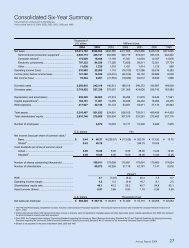
5<br />
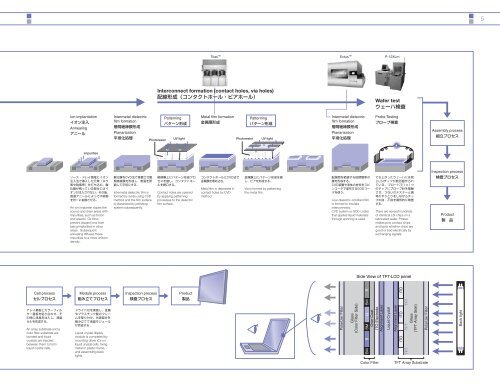
Trias TM Ectus TM P-12XLm<br />
Interconnect formation (contact holes, via holes)<br />
<br />
Wafer test<br />
<br />
Ion implantation<br />
<br />
Annealing<br />
<br />
Intermetal dielectric<br />
film formation<br />
<br />
Planarization<br />
<br />
Photoresist<br />
Patterning<br />
<br />
UV light<br />
Metal film formation<br />
<br />
Patterning<br />
<br />
Photoresist UV light<br />
Intermetal dielectric<br />
film formation<br />
<br />
Planarization<br />
<br />
Probe Testing<br />
<br />
Assembly process<br />
<br />
impurities<br />
Inspection process<br />
<br />
<br />
<br />
<br />
<br />
<br />
<br />
An ion implanter dopes the<br />
source and drain areas with<br />
impurities, such as boron<br />
and arsenic. Ox films<br />
prevent dopant ions from<br />
being implanted in other<br />
areas. Subsequent<br />
annealing diffuses these<br />
impurities to a more uniform<br />
density.<br />
<br />
<br />
<br />
Intermetal dielectric film is<br />
formed by oxide using CVD<br />
method and the film surface<br />
is planarized by polishing<br />
system subsequently.<br />
<br />
<br />
<br />
Contact holes are opened<br />
by applying patterning<br />
processes to the dielectric<br />
film surface.<br />
<br />
<br />
Metal film is deposited in<br />
contact holes by CVD<br />
method.<br />
<br />
<br />
Via is formed by patterning<br />
the metal film.<br />
<br />
<br />
<br />
<br />
<br />
Low-dielectric-constant film<br />
is formed to insulate<br />
interconnects.<br />
CVD system or SOD coater<br />
that applies liquid materials<br />
through spinning is used.<br />
<br />
<br />
<br />
<br />
<br />
<br />
<br />
<br />
There are several hundreds<br />
of identical LSI chips on a<br />
fabricated wafer. Prober<br />
makes pins contact chips,<br />
and tests whether chips are<br />
good or bad electrically by<br />
exchanging signals.<br />
<br />
Product<br />
<br />
<br />
Cell process<br />
<br />
<br />
<br />
<br />
<br />
An array substrate and a<br />
color filter substrate are<br />
bonded and liquid<br />
crystals are injected<br />
between them to form<br />
liquid crystal cells.<br />
Module process<br />
<br />
<br />
<br />
<br />
<br />
<br />
Liquid crystal display<br />
module is completed by<br />
mounting driver ICs on<br />
liquid crystal cells, fixing<br />
metal or plastic frame,<br />
and assembling back<br />
lights.<br />
Inspection process<br />
<br />
Product<br />
<br />
Polarizer Filter<br />
Glass<br />
(Color Filter Side)<br />
BM B BM G BM R<br />
Over Coat<br />
ITO Electrode<br />
Alignment Layer<br />
Liquid Crystal<br />
ITO<br />
Alignment Layer<br />
ITO<br />
TFT<br />
ITO<br />
TFT<br />
TFT<br />
Glass<br />
(TFT Array Side)<br />
Polarizer Filter<br />
Back light<br />
Color Filter<br />
TFT Array Substrate