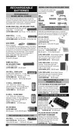
Spec sheet available in PDF format. - All Electronics
Spec sheet available in PDF format. - All Electronics
Spec sheet available in PDF format. - All Electronics

You also want an ePaper? Increase the reach of your titles
YUMPU automatically turns print PDFs into web optimized ePapers that Google loves.
fteface<br />
This user's manuar concem<strong>in</strong>g DMC series has been prepared for all users of oprREx's dot<br />
matrix LcD modures (character type DMC Series) to assist trem <strong>in</strong> design<strong>in</strong>g with the modures<br />
properly and efficiently.<br />
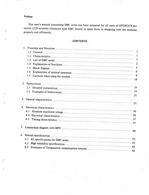
CONTENTS<br />
I . Function and Structurr.<br />
l.t General<br />
I<br />
1.2 I ? Characteristics. fhoer+o;.+i^. . . . . I<br />
""""<br />
I .3 List of DMC series.<br />
I<br />
!.4 Explanation of functions.<br />
2<br />
l'5<br />
.........<br />
Block diagram 3<br />
' .........<br />
I .6 Explanation of <strong>in</strong>temal operation 6<br />
.<br />
1.7 Cautions when<br />
g<br />
us<strong>in</strong>g the module. . . . . ......<br />
lg<br />
2' Instructions'<br />
2.1 Detailedexplanations<br />
.2 Examples of Instructions.<br />
.........r9<br />
"""'25<br />
3. Opticat characteristics .<br />
35<br />
4, Electricalchaftrcteristics<br />
4.1 ....36<br />
Absolute maximum rat<strong>in</strong>gs<br />
4.2 Electrical characteristics 36<br />
43 Tirn<strong>in</strong>g charactedstics<br />
3?<br />
37<br />
5. Connection diagram with MpU<br />
40<br />
6. <strong>Spec</strong>ial specifications. . . . .<br />
6.! EL specifications for DMC 42<br />
series.<br />
6.2 l|lLgh reliability specifications<br />
42<br />
5.3 Examptes of Tcmpcrature 4S<br />
compcnsation ciEuits<br />
-.. . 46
1. FUNCTION AND STRUCTURE<br />
1.1 General<br />
DMC series is the name given to the dot matrix LCD display modules that have recently been<br />
developed by oPTREX coRPoRATloN. The modules consisr of high contrast-large view<strong>in</strong>g<br />
angle TN type LC panel, with a CMOS driver and controller, which have a tow power consump<br />
tion. The controller is equipped with an <strong>in</strong>temal character generator ROM, RAM and RAM for<br />
display data. <strong>All</strong> display functions are controllable by <strong>in</strong>structions mak<strong>in</strong>g the <strong>in</strong>terfac<strong>in</strong>g with<br />
MPU eary.<br />
Both display data RAM and character generator RAM can be read, mak<strong>in</strong>g it possihle to use<br />
any part not used for display as general data RAM. The products of this series therefore have a<br />
wide application possibilities <strong>in</strong> the field of term<strong>in</strong>al display or display for measur<strong>in</strong>g devices.<br />
72 Charactorbtic<br />
(l) 5x TdotstCunor,5x8dotsor5x ll dots, dot matrix LCD (TN mode)<br />
Q, 4 bit or 8 bit <strong>in</strong>terface with MpU is possible<br />
(3) Display data RAM.........80x 8bit(Max 80 characters)<br />
(4) ChaEcter generator ROM. . .Character fonr 5 x 7 dots 160 k<strong>in</strong>ds<br />
Character font 5 x l0 dots 32 k<strong>in</strong>ds<br />
(5) Character generator RA.lrl . . .Program write (64 x g bit)<br />
Character font 5 x 7 dots 8 k<strong>in</strong>ds or<br />
Character font 5 x l0 dots 4 k<strong>in</strong>ds<br />
(6) Both display data RAM and character generator RAM can be read fronr Mpu<br />
(7) Duty ratio... ....t L<strong>in</strong>e Display, llgduty Sx7 dots + Cursor, sxg dors<br />
l/t I duty 5rl I dots<br />
t/16 dury 5xZ dots + Cursor, 5xg dots<br />
(8) Wide variety of operat<strong>in</strong>g <strong>in</strong>structions:<br />
2 L<strong>in</strong>e Display: l/16 duty SxZ dots + Cursor, Sxg dors<br />
4 L<strong>in</strong>e Display: l/16 duty 5r8 dors<br />
Display clear, Cunor home, Dispray oN/oFF, Dispray character br<strong>in</strong>k, cursor shift.<br />
Display shift.<br />
(9) Internal automatic reset circuit when supplied with power.<br />
( l0) Intemal oscillat<strong>in</strong>g circuit<br />
(l l) CMOS process used<br />
( l2) Logic power source: S<strong>in</strong>gle (+5V)<br />
( 13) Operat<strong>in</strong>g temperatur€ range: 0 - +50"C (Standard type)<br />
-20 - +70'C (..H" type)<br />
-1-
1.3 Lbt ot DMC aeries<br />
Table #1<br />
\rtcm<br />
Modcl Nol\<br />
DMC 161064<br />
DMC 16106C<br />
DMc161l7<br />
DMc16128<br />
DMC 16129<br />
DMC l6106B<br />
DMC 16207<br />
DMCl6230<br />
DMC 16433<br />
DMC202l5<br />
DMC 20434<br />
DMC24138<br />
D\ic24227<br />
DMc32l32<br />
DMC32239<br />
DMC32216<br />
DMC4013l<br />
DMC402l8<br />
DMC40440<br />
Display<br />
Format<br />
16 ch.r.ct.D<br />
rll<strong>in</strong>c<br />
15 d||nct t<br />
r I l<strong>in</strong>c<br />
l5 chtnclcrt<br />
x I l<strong>in</strong>c<br />
16 chictcr3<br />
x I l<strong>in</strong>c<br />
15 chrtrclcal<br />
r I l<strong>in</strong>c<br />
16 cll|'|cta$<br />
x I l<strong>in</strong>c<br />
16 ch$.clcr3<br />
x 2 l<strong>in</strong>6<br />
16 ch.trctcE<br />
r 2 l<strong>in</strong>6<br />
16 ch.nctcr.<br />
x 4 l<strong>in</strong>ct<br />
20 ch.t ctctt<br />
r 2 hnc3<br />
20 chrr.ctcts<br />
! 4 l<strong>in</strong>c.<br />
24 ch|'rclq.<br />
rlli'lc<br />
24 ch.nctcr3<br />
Chsncter Font<br />
5x I I dots<br />
5x Sdots<br />
5x 8 dots<br />
5x ?dots + Cursor<br />
Module Size I View Area<br />
wxHrT(rnm)l wxH(mm)<br />
Character Size<br />
wxH(mn)<br />
Dot Size<br />
WrH (mm)<br />
80x36x10 I 64.5x 13 IzxU 0.6x 0.7<br />
80x36x10<br />
80x36x10<br />
l22x33x I I<br />
64.5x l3 &2x5.95 0.6x0.7<br />
54.5x13 3.2x5.95 06x0?<br />
99x 13 4.84x9.66 0.92x1.1<br />
5x 7 dots + Cursor l22x33xll 99x l3 4.84x9.66 0.92x Ll<br />
5x 7 dots + Cursot t30x44xl0 99x l3<br />
5x Sdots<br />
5x 7 dots + Cursor<br />
84x44xl I<br />
tnx44xll<br />
5x 8 dots 87x60xll 61.8x25.2<br />
5x 8 dots<br />
I l6x44x 1l<br />
4.9x 9.5 0.9x 1.05<br />
6lxl6 2.95x5.55 0.55x065<br />
99x24 4.84x9.66 092x1.1<br />
295x4.?5<br />
o 55x055<br />
83xl&6 3.2x5.55 0.6x0.65<br />
5x Sdors | 9&0x60x I I 76x25.2 2.95x4.7 5 0.55x0.55<br />
5x l1 dots<br />
x 2 li!.t 5x Sdors I l8x36xl I<br />
l18x36xl I 93.5x 15.8 9.2x8.2 | 0.6x 0.7<br />
93.5x 15.8 | 3.2x5.55 0.6x0.65<br />
32 clu'.ctcrl<br />
x I lir.<br />
5x I ! dots l?4.5x3lxll 123.5x16.5 | g.zxaz | 0.6x0'7<br />
32 ch{rctcn<br />
r 5x<br />
2 l<strong>in</strong>ca<br />
Sdots l74.5x31xll l4l.0x 16.5 3.45x5.55 0.65x0.65<br />
32 chlrclcF<br />
3.2x5.55 0.6x065<br />
5x Sdots l75x44x 1l 130 x 18.6<br />
x 2 l<strong>in</strong>c3<br />
182x3X5x11 152.5x t 6.5 3.2x8.2 0.6 x<br />
40 dr$tctcn<br />
0.7<br />
r I<br />
5x<br />
l<strong>in</strong>c<br />
1l dots<br />
/O chtlclcrt l82x3X5x 1l l52.5x 16.5 3.2x5.55 0.6x0.65<br />
5x 8 dors<br />
40 chrnctqt<br />
t 4 l<strong>in</strong>ct<br />
5x I dots 200x?0x13 165 x 40 3.2x5.95 0.6 x 0.7<br />
-2-
1.4 Explanation ot functioni<br />
(l) P<strong>in</strong> positions and signal names for<br />
DMC t6t06A, DMC t6l06c, DMC t6t t7,<br />
DMCt6t28, DMCl6t29. DMC t6433.<br />
(2) P<strong>in</strong> positions and signal names for<br />
DMC t61068, DMC t6207, DMC t6230.<br />
DMC202t5. DMC32216.<br />
lilf3----------21<br />
P<strong>in</strong> No. Symbol<br />
I<br />
Vss<br />
2 Vcc<br />
Vee<br />
4 RS<br />
R,/N<br />
b<br />
E<br />
DBO<br />
8 DBI<br />
9 DB2<br />
l0<br />
ll<br />
l2<br />
l2<br />
l4<br />
DB3<br />
DB4<br />
DB5<br />
DB6<br />
DB7<br />
P<strong>in</strong> No.<br />
I<br />
2<br />
Synbol<br />
Vss<br />
Vcc<br />
Vee<br />
4 RS<br />
) R,,W<br />
6 E<br />
7 DBO<br />
8 DBt<br />
I DB2<br />
I<br />
l0<br />
il<br />
t2<br />
l3<br />
l4<br />
DB3<br />
DB4<br />
DB5<br />
DB6<br />
DB7<br />
-3-
(3) P<strong>in</strong> positions snd signal namcs for<br />
DMC24227, DUC24138, DMC32l32,<br />
DMC 32239, DMC 401 3 I, DMC 402 r 8.<br />
(4) P<strong>in</strong> position<br />
DMC40440.<br />
and signal names for<br />
l{<br />
I<br />
I<br />
I<br />
o<br />
OO 13<br />
oo<br />
oo<br />
oo<br />
oo oo oo<br />
i;tl<br />
roo| |<br />
roo I<br />
'oo .oql<br />
I<br />
rod :<br />
'Oo.:<br />
;i;, i<br />
P<strong>in</strong> No. Symbol<br />
I<br />
Vss<br />
2 Vcc<br />
a<br />
Vee<br />
4 RS<br />
J<br />
o<br />
R/W<br />
E<br />
7 DBO<br />
8 DBI<br />
o<br />
l0<br />
tl<br />
r2<br />
l3<br />
l4<br />
DB2<br />
DB3<br />
DB4<br />
DB5<br />
DB6<br />
DB7<br />
P<strong>in</strong> No. Symbol<br />
I<br />
DB7<br />
2 DB6<br />
J<br />
DB5<br />
4 DB4<br />
D<br />
DB3<br />
6 DB2<br />
7<br />
DBl<br />
I<br />
l0<br />
ll<br />
DBO<br />
9 E<br />
r2<br />
l3<br />
t4<br />
IJ<br />
l6<br />
F/W<br />
RS<br />
Vee<br />
Vss<br />
Vcc<br />
LS<br />
NC<br />
-{-
Trbh #2 List of term<strong>in</strong>al tunctions<br />
Signal name<br />
Number<br />
of l<strong>in</strong>e<br />
Input/<br />
output<br />
Connected<br />
to<br />
Function<br />
DB4 - DB7<br />
4<br />
Input/<br />
output<br />
MPU<br />
4 l<strong>in</strong>es of high order data bus. Tristate, bidirectional.<br />
Tramfer of data between MPU and<br />
module is done tlrough these l<strong>in</strong>es. Also DB7<br />
can be used as busy flag.<br />
DBO - DB3<br />
lnput/<br />
output<br />
MPU<br />
4 l<strong>in</strong>es of low order data bus, Tristate. bidirectional.<br />
Transfer of data between MPU and<br />
module is done through these l<strong>in</strong>es. However <strong>in</strong><br />
case of4 bit operation, they are not used.<br />
E I Input MPU Operation start signal for data read/write.<br />
Rnv<br />
I Input MPU<br />
Signal to select Read (R) or Write (lV)<br />
"0" : Write<br />
"l " : Read<br />
RS<br />
I Input MPU<br />
Signal to select register<br />
"0" : Instruction register (Write)<br />
: Busy flag; Address counter (Read)<br />
"1" : Data register (Write, Read)<br />
LS<br />
I Input MPU<br />
Signd to select l<strong>in</strong>e of display panel. This<br />
term<strong>in</strong>d is for DMC 40t140 only.<br />
"1" : To select upper 2l<strong>in</strong>es<br />
"0" : To select lower 2 l<strong>in</strong>es<br />
Vce<br />
I<br />
Power<br />
supply<br />
Term<strong>in</strong>al for LCD drive power source<br />
Vcc<br />
I<br />
Power<br />
supply<br />
+5V<br />
Vss<br />
I<br />
Power<br />
supply<br />
0v (GND)<br />
-5-
EI<br />
IE<br />
ri<br />
!F<br />
I<br />
o<br />
t<br />
I<br />
e<br />
F<br />
t t<br />
E3<br />
q<br />
a<br />
lr.<br />
,lt<br />
llr<br />
JiJ grr<br />
-6-
Ei<br />
8:<br />
JE<br />
si<br />
E:<br />
6e<br />
B<br />
F<br />
C'<br />
:<br />
C)<br />
x<br />
a<br />
I<br />
o<br />
EI<br />
o o<br />
-7-
1,6 Explanation of <strong>in</strong>temal operation<br />
(l) Register<br />
The Controller for the DMC series has 2 k<strong>in</strong>ds of 8 bit registen, which are the<br />
Instruction register (IR) and the data register (DR).<br />
IR is a register to store <strong>in</strong>struction codes tike Display Clear or Cursor Shift as<br />
well as address <strong>in</strong><strong>format</strong>ions for disptay data RAM (DDRAM) or character generator :<br />
RAM (CG RAjr{).<br />
IR can be written from MPU but cannot be read by the MpU.<br />
DR is a register used for stor<strong>in</strong>g temporarilly data to be wdtten <strong>in</strong>to DD RAM or<br />
CG RAM and data to be r€ad out from DD RAM or CG RAM.<br />
Data written <strong>in</strong>to DR from Mpu is automatically written <strong>in</strong>to DD RAM or cG<br />
RAM by <strong>in</strong>temal operation.<br />
AIso DR is used to store data when read<strong>in</strong>g out data from DD RAM or cG I{AM.<br />
when addres <strong>in</strong><strong>format</strong>ions ar€ written <strong>in</strong>to tR, data is read out from DD RAM<br />
or CG RAM to DR by <strong>in</strong>ternal operation.<br />
Data transfer to the MpU is then completed by the MpU reach<strong>in</strong>g of DR.<br />
After MPU reads DR, data <strong>in</strong> the DD RAM or cG RAM at the next address rs<br />
sent to DR for the next read from the MpU. Register selector (RS) signals make<br />
their selection from these two registers.<br />
I<br />
Table #3 S€l€ction of registers<br />
RS<br />
R/w<br />
OPERAT|OI\i<br />
0<br />
0<br />
IR write, <strong>in</strong>temal operation (Display Clear etc.)<br />
0 I<br />
Bury0ag @Bz ) and address counter (DBo - DBe ) read<br />
I 0<br />
DR Write, Intemal Operation (DR* DD RAM or CG RAM)<br />
I<br />
I<br />
DR Read, Intemal Operation (DD RAM or CG RAM)<br />
-8-
(2\ Busy flag(BF)<br />
When the Busy Flag is "1", the module is <strong>in</strong> the <strong>in</strong>ternal operation and the next<br />
<strong>in</strong>struction will not be accepted. As shown <strong>in</strong> the Table #3, the busy flag outputs to<br />
DBr when RS=o, RA =I. The next <strong>in</strong>struction must be written after ensur<strong>in</strong>g that<br />
the busy flag is "0".<br />
(3) Address Counter (AC)<br />
The address counter (AC) assigns address to DD RAM and CG RAM'<br />
When an <strong>in</strong>struction for address is written <strong>in</strong> IR, the address <strong>in</strong><strong>format</strong>ion is sent<br />
from IR to AC. The selection of either DD or CG RAM is also determ<strong>in</strong>ed concurrently<br />
by the <strong>in</strong>struction.<br />
After writ<strong>in</strong>g <strong>in</strong>to (read<strong>in</strong>g from) DD RAM or CG RAM display data, address<br />
counter (AC) is automatically <strong>in</strong>cremented by +l (or decramented by -l ). AC<br />
contents arc outputted to DBo - DBr when RS=0 and R/Wl as shown <strong>in</strong> Table<br />
(4) Display data RAM (DD RAM)<br />
The disptay data RAM stores display data represented <strong>in</strong> &bit character code. Its<br />
capacity is 80 x 8 bits or 80 characters. The display data RAM that is not used for<br />
display can be used as a general data RAM.<br />
Relations between DD RAM addresses and positions on the LCD are shown<br />
below.<br />
The DD RAM addrcss (ADD) is set <strong>in</strong> the Address Counter (AC) and is represented<br />
<strong>in</strong> hexadecimal notation.<br />
MSB<br />
LSB<br />
AC:<br />
Hcxrdccimd<br />
Hcxrdecimal<br />
lErample 1l DD RAM sddrgs '?E"<br />
I 0 0 I I 0<br />
E<br />
-9-
[Example 2] 4O columnr I t<strong>in</strong>e disptay (DMg0Ol3il<br />
Column<br />
t2<br />
I l<strong>in</strong>€<br />
lJ<strong>in</strong>e<br />
z.|ne<br />
Column<br />
t2345<br />
t4 15 t6<br />
00 0l 02 03 04 OD OE OF<br />
40 4l 43 44 4D 4E 4F<br />
_ Diglay<br />
column<br />
.<br />
DD RAM<br />
Address<br />
When the display shift is pcrformed DD RAM address moves as follows<br />
0l 02 03 04 05 OE OF t0<br />
Left shifi<br />
4l 43 44 45 4E 4F 50<br />
00 0l 02 03 0c OD OE<br />
Righr shifr<br />
67 40 4l 42 43 Q 4D 4E<br />
Other 2-l<strong>in</strong>e display modules movc the same wav.<br />
ftJ<strong>in</strong>e<br />
uppe4<br />
8-l<strong>in</strong>c<br />
[Example 4] 40 columnr 4 t<strong>in</strong>rr dilphy (DMC40[4OI<br />
In case of DMC4O440, the display is similar to 40 columns 2 l<strong>in</strong>es and it is used<br />
by switch<strong>in</strong>g the upper trro r<strong>in</strong>es and lower two l<strong>in</strong>es by LS signars. Therefore<br />
the relation between DD RAM and display columns is as follows:<br />
Column<br />
t2345<br />
- Displey<br />
column<br />
39 40<br />
00 0t 02 03 u 26 )1<br />
40 4l 42 43 44 66 67<br />
*<br />
DD RAM<br />
Address<br />
Ie-r<strong>in</strong>e<br />
Lowcrf<br />
[4.l<strong>in</strong>e<br />
m 0l 02 03 u 26 'l'l<br />
40 4l 42<br />
'l *l loo 67<br />
.<br />
DD RAM<br />
Addrcs.s<br />
-11-
when LS = ..1" (select<strong>in</strong>g upper l<strong>in</strong>es) and shift<strong>in</strong>g the display to the right, the<br />
DD RAM address moves as follows:<br />
Uppcr<br />
{Hhc<br />
[2{<strong>in</strong>c<br />
3-l<strong>in</strong>c<br />
4J<strong>in</strong>c<br />
1., 00 0t 02 03<br />
,'<<br />
26<br />
67 40 4l 42 43 55 66<br />
00 0r 02 03 04 26 27<br />
zl0 4l 42 43 4 66 67<br />
lffhen LS = *0" (tower l<strong>in</strong>e selection) and disptay is shifted to the riSht' DD RAM<br />
address moves as follows:<br />
Uppcr<br />
l -l<strong>in</strong>c<br />
2-l<strong>in</strong>c<br />
00 0r 02 03 (X 26<br />
40 4l 42 43 4 66 67<br />
[rl<strong>in</strong>c<br />
lrwcrl<br />
[4-l<strong>in</strong>c<br />
11 00 0l 02 03 25 26<br />
67 4 4l 42 43 65 66<br />
In case of DMC40440, it can be considered as a module comb<strong>in</strong><strong>in</strong>g 2 modules of 40<br />
cotumns2l<strong>in</strong>esdisplay.Horreverslrift<strong>in</strong>gthe4l<strong>in</strong>esatthesametimeisnotpossible.<br />
hiortowrit<strong>in</strong>g<strong>in</strong>structionitisnecesarytospecifyeithertheuppet2.l<strong>in</strong>eorthe<br />
lower 2l<strong>in</strong>e us<strong>in</strong>g the LS sienal.<br />
[Exrmple5l16columnrll<strong>in</strong>cdirphy{1/16dutyt;dndhplaywillbca:follow::<br />
l -l<strong>in</strong>c<br />
Column<br />
123 89<br />
14 t5 16<br />
00 0l 02 o7 40 45 46 47<br />
-Disptay<br />
column<br />
.DD RAM<br />
Address<br />
-t2-
(5) Orancter gencrator ROM (CG ROM)<br />
The character generator ROM (CG ROM) is a ROM capable to generate from<br />
&bit character code, 5 x 7 dots or 5 x l0 dott chancter pattem.<br />
The said ROM can getrerate 160 k<strong>in</strong>ds of 5 x ? dots or 32 k<strong>in</strong>ds of 5 x l0 dots<br />
character pattems.<br />
Howevcr cautions ane requested whcn opcrat<strong>in</strong>g this RoM because those character<br />
fonts of 5 x 7 dots of the modurc will not be displayed after the gth row of 5 x<br />
l0 dots charecter pattem.<br />
Also this RoM can be modified to gpnerate character pattem of our users<br />
choice.<br />
For further der'its, please contact OpTREX sates depanmenr.<br />
(6) Character generator RAM (CtG RAM)<br />
The character generator RAM is the RAM with which the user can rewrite<br />
charactet patterns by program.<br />
With 5 x 7 dots 8 types of character patt€rns can be written. To display character<br />
pattems stor€d <strong>in</strong> cG RAM write tre chrracter codes <strong>in</strong> the reft corumn of rabte<br />
5.1 and 5.2 <strong>in</strong> the DD RAM conespond<strong>in</strong>g to the display position.<br />
The relations between CG RAM address and data and disptayed pattem are<br />
shown <strong>in</strong> Table #5.1 and 5.2 respectivcly.<br />
Besides, at€a not used for disptay can be used as general data RAM,<br />
-13-
T$h #4 Co.?..poda|u b.ttraaai Cl|'-tat Godaa atd aliral.r p'ntln'<br />
------__{otu,r 0000 ml0 00ll 0t00 0l0l 0||0 0lll t0t0 l0tl ||00 0l t0 ||tl<br />
I:i<br />
I<br />
..!l<br />
I<br />
:.I<br />
! x \00o I<br />
rl -!!!__r__!!:__-L!,___i<br />
I i:-l<br />
xxxr0.0l<br />
yr!r00t0<br />
-T'jI<br />
T-T<br />
3.<br />
;:l<br />
tl<br />
H : .-..1<br />
!l<br />
.-'l<br />
5 ;I<br />
T<br />
-il<br />
;l<br />
I<br />
!!!___-L ..1..1<br />
\ml I<br />
-:l i.:'l ':'i I3 '--T<br />
t:'! |<br />
il<br />
.!".<br />
: .l<br />
I<br />
I<br />
__!=J<br />
-'l =!-l<br />
:F-T<br />
-T<br />
x 0ro<br />
_+'_l I tt-. ITl _!l .ii<br />
il ..1<br />
__!=l __-:-tIj<br />
-!+ :'i 'i": ::<br />
I<br />
:<br />
t r x ^0101<br />
EI<br />
'6,<br />
i_j :_.i<br />
-FTFI -r.t<br />
r x x x0lt0<br />
;<br />
1.r I:I] ..,.1 ...1<br />
, x x tol lt<br />
4 x r1000<br />
, r xl00l<br />
r!i<br />
F'lF : tl<br />
I 1. :l -I<br />
1<br />
.-l<br />
:l<br />
r<br />
I i: ? t_.1 *t ?<br />
?<br />
r3)<br />
rrt/t0t0 .l<br />
xtxrll00<br />
t5l .|<br />
! x r x lllC<br />
x tl<br />
(5)<br />
Ī<br />
(l)<br />
'T.<br />
:JTi<br />
---t -": I<br />
.31<br />
.t<br />
i.r:<br />
I<br />
+.<br />
t!<br />
-* $<br />
? -. 1<br />
,* I<br />
i"<br />
r-1 tt. FI<br />
f,l<br />
I t' il t t<br />
! r1 -+ 1: llr n<br />
(a)<br />
J ft + ttl<br />
r.<br />
l -l tr<br />
r:t<br />
(Norc) Ch.nc&r ofhiSh ordct b lII0|t|dIIII<br />
v bc hd'qurt'<br />
-14-
Table #5.1 Rolation bd r€on CG RAM !ddr6s, chlrac'tor codes (DD RAM) and cfiaracter<br />
p.ttsms (CG RAM datrl (<strong>in</strong> cat. of 5 x 7 dotsl<br />
Nob: (l)<br />
(2)<br />
(3)<br />
(4)<br />
(s)<br />
765{3210<br />
0 0 0 0*0 0 0<br />
0000*001<br />
0000r
Tablc #52 RolEtion betvcan CG RAM addns, .$attcr codes (DD RAM) and chanctor<br />
pattoms (CG RAM ddal {<strong>in</strong> caro of 5 x l0 doal<br />
76543210<br />
- HiShGr ordq Loc/at ordct.<br />
bir bir<br />
-<br />
0000'k00*<br />
3..?<br />
"l*9i.-<br />
0000<br />
0001<br />
00t0<br />
001I<br />
0100<br />
0l0t<br />
0l t0<br />
0l r I<br />
t 000<br />
1001<br />
t0t0<br />
l0l<br />
| 100<br />
I l0l<br />
I l l0<br />
lllt<br />
I<br />
000<br />
000<br />
000<br />
000<br />
*+x**<br />
I<br />
I<br />
I<br />
*****<br />
00<br />
00<br />
00<br />
0<br />
0<br />
0<br />
0<br />
0<br />
Exrmplr of chia.clcr<br />
Prttcm<br />
Crrlor politio.r<br />
0000*ll*<br />
t rlt 0 0 I<br />
Ir o r o<br />
__1: _"_ : _<br />
t0lt<br />
l100<br />
I l0l<br />
I I l0<br />
ltll<br />
----i-------<br />
* * *r* * * * *<br />
I<br />
I<br />
i<br />
***x*<br />
.mGlnl<br />
Do!'t crrc.<br />
Noto: (l) Ch.racter code bits l,2correspond to CG RAM address bits4,5 (2 bits: 4 typ6)<br />
(2) CG RAM address bits 0 - 3 designate character l<strong>in</strong>e position.<br />
The I I th l<strong>in</strong>e is the ornor position and display is performcd <strong>in</strong> logical OR with<br />
cul50r.<br />
Ma<strong>in</strong>ta<strong>in</strong> the I lth l<strong>in</strong>e correspond<strong>in</strong>g to the cursor display position <strong>in</strong> the "0" state<br />
for cursor display.<br />
When the I lth l<strong>in</strong>e data is "1", bit I lights up regardless of cursor existcnce.<br />
(3) Character pattern row positions are the same as 5 x 7 dot character pattern posi'<br />
tions.<br />
(4) As shown <strong>in</strong> Table 5.2 CG RAM charactcr pattems arc selected when character code<br />
bits 4 - 7 are all "0". However, s<strong>in</strong>cc character code bit 0 and 3 are <strong>in</strong>effective bits,<br />
the display of charactd pattem exarnple is selected by character code "00" "Ol"<br />
"08" "09" (Hexadecimal)<br />
(5) "!" for CG RAM data corresponds to selection for display and "0" for non'sclec'<br />
tion.<br />
-16-
Table #6 List of <strong>in</strong>struc{ionr<br />
halruction<br />
Codc<br />
Excc!tion timc<br />
Dc.cription<br />
(irl.x)<br />
RS Rnp DBr DR. DBs DB- DBr DBo<br />
(when fcp o.<br />
fosc is 250kHz)<br />
Ocar<br />
Di.phy<br />
0 0 0 0 0 0 0 0 0 I<br />
Clcst!.ntir. di.pl.y |od s.ls DD<br />
RAM rddrc.s 0 <strong>in</strong> rddllt counrcr.<br />
l.64ms<br />
Srt DD RAM.ddrc$ 0 ir ddrcrs<br />
Ralutr!<br />
Hornc<br />
0 0 0 0 0 0 0 0 I countcr. Abo artumt dirphy bc<strong>in</strong>r<br />
rhifacd ro oria<strong>in</strong>sl po.ition. DD RiM l-64ms<br />
contcn$ rcma<strong>in</strong> unch$tcd.<br />
Slti curtor movc dlrcclion and<br />
Enry<br />
odc<br />
0<br />
Sct<br />
0 0 0 0 0 0 I tlD s<br />
tpccificr .hifr of di$by.<br />
Th6c opcrations att pcrformcd duriD8<br />
d.|| f,,rile rnd rcrd.<br />
40rs<br />
Disphy<br />
Scc ON/OFF of.nrjF ditgl.y (D).<br />
ON/OFF o 0 0 0 0 0 I D c a cunor ON/OFF (C), rnd<br />
Control<br />
bl<strong>in</strong>k of<br />
cur3or position ch.r.ct.. (B).<br />
40|rs<br />
Clrtor or<br />
Dirpby 0 o 0 0 0 I src R/L<br />
lloucr c||rtor .nd rhiflr dilDhv vithouI<br />
ch.u<strong>in</strong>s DD RAI{ conic;rs.<br />
4otls<br />
Shifr<br />
Function<br />
Scts <strong>in</strong>tcrface drrr l.nrth (DL).<br />
S€t<br />
0 0 0 0 DL N F<br />
numb.r ofdilpLy l<strong>in</strong>6 (L) .nd<br />
chrncicr fonr (F).<br />
40!r<br />
S.T CG RAM<br />
Addrcs 0 0 0 I AGC S.t, CG RAM sddtltr. CG RAM d.r.<br />
is tcnt rttd rrctivcd rficr this lctt<strong>in</strong>&<br />
4Opr<br />
Srr DD RAM<br />
Addr.rs 0 0 I ADD Scl' DD RAM.ddl€3!. DD RAM dal.<br />
ia tant and rcceivcd aftGr thia scn<strong>in</strong>S. 40/s<br />
Rc.d<br />
Bury Flr3 0 I BF<br />
icdr luty fl4 (BF) iidic.riDg<br />
AC mlclnrl opcr.tion<br />
& Addrlr.<br />
it bc<strong>in</strong>a Dcrfonnd<br />
ard trrd! rddrasr countci contcntr.<br />
40rs<br />
Writ. D!t.<br />
to CG or 0 Writc D.te<br />
Writer d.tr <strong>in</strong>to DD RAM or CG<br />
DD RAM<br />
RAM.<br />
40ts<br />
Rc.d D.r.<br />
fron CG ot I Rc.d lhra Rc.dr dj. frorn DD RAM or CC<br />
DD RAM<br />
RAM.<br />
4Ors<br />
UD.l Incrcmcnt<br />
DD RAM : Di.phy drt. RAM<br />
UD-o Exccution<br />
Dlctdn?nt<br />
timc<br />
CG RAM : Ch{.cacs gstrcr.tor RAM chan8cs whcn<br />
3Ar ACt : CE RAM<br />
$STltf,,firdiebv'hirt'<br />
dd'llr fraquancy chenSca.<br />
S/C.{ ADD : DD RAM rddrr$. (Ex.mDlc)<br />
Ctror movc<br />
Cortlgotrdt to c||raor<br />
R/L=l<br />
l{hcn Shifi ro<br />
fcp or forc<br />
rh. rilhr.<br />
.ddIl$.<br />
R/L.o il 27OkHz:<br />
Shifrr io rhc Efr-<br />
DL=l<br />
AC : Addrcat countcr u,cd<br />
8 bib, DL.o : 4 bits.<br />
for borh DD<br />
N-l<br />
md Cc<br />
2l<strong>in</strong>6, N.0: I lit|a<br />
,101s<br />
RAlrl .ddrcrt.<br />
r 2!! - 37r,<br />
F=l<br />
5rl0 dor., F.0: 5r7 dot!<br />
210<br />
BF-l Intcmdly oDcnrilr<br />
BF.0 : C:n.cccgf iurrucdon<br />
-17-
1.7 Cautionr when us<strong>in</strong>g the moduh<br />
( I ) LCD panel is made of glas so plcase 8void subject<strong>in</strong>g to strong mechanical shock<br />
or apply<strong>in</strong>g strong pressurc on to the surface of display area.<br />
(2) The polarizcr used on the surface of display panel is easily scratched and<br />
2<br />
damaged. Therefore please be careful when handl<strong>in</strong>g the module.<br />
(3) CMO$LSI is uscd for module circuit therefore your attention is called to the<br />
follow<strong>in</strong>g:<br />
I ) <strong>All</strong> unused <strong>in</strong>put tem<strong>in</strong>als should bc connected to Vcc or GND. The selection of<br />
Vcc or GND will depend upon which connection will satisfy the desircd logical<br />
function.<br />
2) Wh* power sourcc voltage is not applied avoid apply<strong>in</strong>g <strong>in</strong>put signal.<br />
3) Anti-static etectricity measules<br />
a. When work<strong>in</strong>g pleasc bc sur€ to either use your naked or gloved hand and<br />
wear non
2. TNSTRUCTIONS<br />
2,1 Detailedexplanations<br />
(t) Clear Display<br />
RS R,/W DB'<br />
0 010 0 0 0 0 0 U I<br />
DBo<br />
Writes the space code "20" (hexadecimal) <strong>in</strong>to all address of DD RAM. Retums<br />
display to its orig<strong>in</strong>al position if it was shifted. In other words the display disappears<br />
and tlte cursor or bl<strong>in</strong>k moves to the left edge of the display (the first l<strong>in</strong>e if 2l<strong>in</strong>es<br />
are displayed). The ex€cution of clear display <strong>in</strong>struction sets entry mode to <strong>in</strong>crement<br />
mode.<br />
(2') Retum Home<br />
RS R,,/W DBT<br />
0 0 0 0 0 0 0 0 I<br />
rmcans Don't care<br />
Sets the DD RAM address "0" <strong>in</strong> address counter. Retum display to its orig<strong>in</strong>al<br />
position if it was strifted. DD RAM contents do not change.<br />
The cursor or the bl<strong>in</strong>k moves to the left edge of the display (the first l<strong>in</strong>e if 2<br />
l<strong>in</strong>es are displayed)<br />
(3) Entry mode set<br />
RS S,/W DBT<br />
DBo<br />
Codc<br />
0 0 0 0 0 0 0 I T,/D S<br />
UD:<br />
S:<br />
Increments (I/D = l) or decrcments (ID = 0) the DD MM address by I<br />
when a character code is written <strong>in</strong>to or read from the DD RAM.<br />
The cunor or bl<strong>in</strong>k movcs to the right when <strong>in</strong>cr€mented by +1.<br />
The same applies to writ<strong>in</strong>g and read<strong>in</strong>g of CG RAM.<br />
Shifts the entire display either to the right or to the left when S = I ; shift to<br />
the left when l/D = | and to the right when l/D = O. Thus it looks as if the<br />
cutsor stands still and only the display seelns to move.<br />
The display does not shift when read<strong>in</strong>g from DD RAM nor when S = 0.<br />
- 19-
(4) Display ON/OFF Control<br />
RS R,/W DBI<br />
Codc<br />
0 0 0 0 0 0 I D L B<br />
D:<br />
C:<br />
B:<br />
The display is ON when D = t and OFF when D = 0. When OFF due to D =<br />
0, display data rema<strong>in</strong>s <strong>in</strong> the DD RAM. It can be displayed immediately by<br />
sett<strong>in</strong>g D = l.<br />
The cursor ilisplays when C = I and does not display when C = 0.<br />
Even if the cursor disappears, the function of I/D ctc, does not change<br />
dur<strong>in</strong>g data write.<br />
The cursor is displayed on the 8th l<strong>in</strong>e whcn 5 x 7 dot character font has<br />
been selected.<br />
The character <strong>in</strong>dicated by cursor bl<strong>in</strong>ks when B = I . The bl<strong>in</strong>k is displayed<br />
by switch<strong>in</strong>g between all blank dot and display characters at 0.4 sec<br />
<strong>in</strong>terval.<br />
The cursor and the bl<strong>in</strong>k can be set to display simultaneously.<br />
ltttl<br />
IIII<br />
anlr<br />
LI<br />
-<br />
5x7dot<br />
L Ufl'T<br />
-I<br />
rrrrn<br />
r-<br />
rlil<br />
tttl<br />
tttl<br />
FTNI<br />
LLI LI<br />
LIJ<br />
5 x l0 dots<br />
chffrctcr font drsrect3r font<br />
H*I<br />
CEEED I<br />
Alt€rnrt<strong>in</strong>g display<br />
(a) Curror displey exemplc<br />
(b) Bl<strong>in</strong>k display cxamplc<br />
(5) Cursor or display shift<br />
Codc<br />
RS R,/WDBI<br />
0 0 0 0 0 I 3/C R.L<br />
DBo<br />
.mcrnt Don't carc.<br />
-20-
(5) g*561 q1 display shift<br />
Shifts cunor position or display to the rieht or laft without writ<strong>in</strong>g or read<strong>in</strong>g<br />
display data. This function is used to corect or search for the display. In a 2-l<strong>in</strong>e<br />
display the cursor movrs to the 2nd l<strong>in</strong>e when it passes the 40th digit of the tst l<strong>in</strong>e.<br />
Notice that thc lst and 2nd l<strong>in</strong>e displays will shift at the satne time.<br />
When the disptaycd data is shifted repeatedly each l<strong>in</strong>e only moves horizontally<br />
but the 2nd l<strong>in</strong>e display do€s nor shift <strong>in</strong>to the lst t<strong>in</strong>e position.<br />
s/c<br />
R/L<br />
0 0 Shifc currcr pcition to the teft (AC is decremented by one)<br />
0 t Shifts cunor pcition to thc right (AC is <strong>in</strong>cremented by one)<br />
I 0 Shifts the cntirc dbplay to the lcft. The cursor follo*s the display shift.<br />
I I Shifts the entire display to the right. The cunor follons the display shift.<br />
The contents of Addrcss Counter (AC) do not ch$ge if the only action p€rformed<br />
is sltift<strong>in</strong>g dtsphD'.<br />
(6) Function s€t<br />
(a) l -l<strong>in</strong>e display<br />
RS R,/W DBI<br />
DBo<br />
0 0 0 0 I DL 0 F<br />
rrncrnr Don't crrc<br />
(b) 2{<strong>in</strong>e display<br />
RS R,ZW DBI<br />
DBo<br />
Codc<br />
0 0 0 0 DL I<br />
. mc|ns l)on't€atc<br />
-21-
DL: Sets <strong>in</strong>terface data lcndh. Data are sent or received <strong>in</strong> 8 bits lengfh (DBr -<br />
DBo ) when DL='l 'and <strong>in</strong> bits length (DB, - DBr) when DL= 0.<br />
When the 4 bits length is selccted, data must be scnt or rcccived twice.<br />
F: Scts character font.<br />
F="1":5xl0dots<br />
F="0":5x7dots<br />
Nots: l) Perform thc function at the head of the program befort execut<strong>in</strong>g all<br />
<strong>in</strong>structions (except "Busy flagfaddress read). From this po<strong>in</strong>t, the function<br />
sct <strong>in</strong>struction cannot be executed other than to changs <strong>in</strong>terface<br />
lcngth.<br />
2) lilhcn powcr srpply b applied the follow<strong>in</strong>g <strong>in</strong>itial sctt<strong>in</strong>g is automaticdly<br />
set r€grdlcss of typcs of modules.<br />
(i) Display clear<br />
(ii) Function set<br />
Intcrfacc data length 8 bits<br />
l.l<strong>in</strong>e display<br />
(iii) Display ON/OFF Control<br />
Display OFF, Cursor OFF, Bl<strong>in</strong>k OFF.<br />
(iv) Entry mode set<br />
No <strong>in</strong>clement or shift.<br />
Therefore <strong>in</strong> case of 2 (4) l<strong>in</strong>es display module, it is necessary to<br />
excute function sct ag<strong>in</strong>.<br />
3) To correctly operate the <strong>in</strong>itial sett<strong>in</strong>g the follow<strong>in</strong>g condidons for the<br />
powcr sounoe ar€ necessary.<br />
0.1 n|s lna<br />
(7) SetCG RAM address<br />
. Toff stipulates the time of power OFF for power supply iNtantaneous<br />
cut off or when the power supply repeats ON/OFF.<br />
If the above conditions are not satisfied automatic <strong>in</strong>itid sett<strong>in</strong>g cannot<br />
be pcrformed. In that casc cxecute <strong>in</strong>itial sett<strong>in</strong>S with <strong>in</strong>structions.<br />
Codc<br />
RS R,/W DBT<br />
0 0 0 A A A A A A<br />
lrwcr ordcr bit3-<br />
t H$hcr odcr bits<br />
-22-
(8)<br />
Sets CG RAM address <strong>in</strong>to the address counter <strong>in</strong> b<strong>in</strong>ary AAArq,rArd{ and then<br />
data is written or read from the MPU for the C13 RAM.<br />
Set DD RAM address<br />
._ Htghcr order bits l,ow€r order bits<br />
-<br />
sets the DD RAM address <strong>in</strong>to tre address counte! <strong>in</strong> b<strong>in</strong>ary A./4'JA,r4,./dqA Data is<br />
then written or read from the MPU for the DD RAM.<br />
Howwer, for l-l<strong>in</strong>e display module fuq,/q'rdqi./M is "00" - '?F" (hexadecimal)<br />
for 2{<strong>in</strong>e display module AAAAAAA is 't00" - "27" (hexadecimal) for the f<strong>in</strong>t<br />
l<strong>in</strong>e and "40" - "67" (hexadecimal) for the second l<strong>in</strong>e.<br />
(9) Read busy flag and addrrs<br />
RS R,/W DBT<br />
DBo<br />
Codc<br />
0 I ts A A A A A A<br />
-<br />
Reads the busy flag (BF) that <strong>in</strong>dicates the system is none <strong>in</strong>ternally operat<strong>in</strong>g<br />
by a previously received <strong>in</strong>struction. BF = I <strong>in</strong>dicates that <strong>in</strong>ternal operation is <strong>in</strong><br />
progress and the next <strong>in</strong>stnrction will not be accepted untit BF is set to ..0".<br />
Check the BF status bcfore the next write operation.<br />
At the same time the value of the address counter expressed <strong>in</strong> b<strong>in</strong>ary<br />
AAAAAAA is r€ad out. The address countcr is used by both CG and DD RAM and<br />
its value is determ<strong>in</strong>ed by the prcvious <strong>in</strong>stnrction. Addrcss contents are the same as<br />
<strong>in</strong> items (7) and (8).<br />
(10) Write data to Cc or DD RAM<br />
RS R,/W DBT<br />
Codc<br />
0 D D D D D D D D<br />
-<br />
Higher ordcr bits l.oscr order bits -<br />
Hthcr order bir Lowcr ordcr bits-<br />
-23-
Writes b<strong>in</strong>ary 8 bits data DDDDDDDD to the Ci|3 or DD RAM.<br />
The previous designation determ<strong>in</strong>es whether t}re CG or DD RAM is to b€ read<br />
(CG RAM address set or DD RAM address set). After a write the entry mode will<br />
automatically <strong>in</strong>creases or decreases the address by l. Display shift also follows the<br />
ertry mode.<br />
(l l) Read data from CGoTDD RAM<br />
RS RzzW DBr<br />
DBo<br />
Code<br />
I I D D l) D D D D D<br />
- Higher ordcr bits L,ower ordcr bils -<br />
Reads b<strong>in</strong>ary 8 bits data DDDDDDDD from the CG RAM or DD RAM.<br />
The previous designation detem<strong>in</strong>es whether the CG or DD RAM is to be read.<br />
Before enter<strong>in</strong>g the read <strong>in</strong>struction, you must execute either the CG RAM or<br />
DD RAM addres set <strong>in</strong>struction.<br />
If you don't, the first read data will be <strong>in</strong>validated. When serially execut<strong>in</strong>g the<br />
"read" <strong>in</strong>struction the next address data is normally read from the second read.<br />
The "address set" <strong>in</strong>struction need not be executed just before the "read"<br />
<strong>in</strong>struction when shift<strong>in</strong>g the cursor by cursor shifl <strong>in</strong>struction (when read<strong>in</strong>g out<br />
DD RAM). The cusor shift <strong>in</strong>struction operation is the same as that of the DD RAM<br />
address set <strong>in</strong>struction.<br />
After a read, the entry mode automatically <strong>in</strong>creases or decreases the address by<br />
l. However display shift is not executed no matter what the entry mode is.<br />
Note: The address counter (AC) is automatically <strong>in</strong>cremented or decremented by I<br />
after "write" <strong>in</strong>structions to either CG RAM or DD RAM. RAM data<br />
selected by the AC cannot then be read out even if "read" <strong>in</strong>structions are<br />
executed.<br />
The conditions for correct data read out arc: execute either th€ address set<br />
<strong>in</strong>struction or cursor shift <strong>in</strong>struction (only with DD RAM) or the execution<br />
of the "read' <strong>in</strong>struction from the second time when the read <strong>in</strong>struction is<br />
serial.
2.2 Examples of <strong>in</strong>structions<br />
(l) Us<strong>in</strong>g DMC l6l06C DMC 16129, DMC l6l068 (l-l<strong>in</strong>e display)<br />
No. lnttruction i Displ.y Op.ration<br />
Powcr upply ON<br />
( lnitializ,edby )<br />
\ lnt€rnal resct circuit /<br />
ffi<br />
Module is <strong>in</strong>itislizcd.<br />
No display appean.<br />
2<br />
Function s€t<br />
RslRAvlDB? -<br />
I lo o t I O 0..<br />
Displey ON/OFF Control<br />
DBo<br />
Sets <strong>in</strong>terface data length and<br />
selects 5 xTdots l.l<strong>in</strong>c dis<br />
Play<br />
Turns on display and corsor.<br />
No display .ppears<br />
R Sl R/w<br />
DBr<br />
0 000 t I t 0<br />
4<br />
Entry mode set<br />
-<br />
RAv<br />
DBr<br />
00000tr0<br />
Sels modc to <strong>in</strong>crcment the<br />
address by one aod to shift<br />
cursor to the right at the time<br />
of write to <strong>in</strong>tcrnal RAM.<br />
5<br />
Writc data to CC/DD RAM<br />
L-<br />
Writes "L" cursor is <strong>in</strong>cremented<br />
and moves to the<br />
right.<br />
t | 0 l0 r 0 0 I r 0 0<br />
Writc d8la ro CC/DD RAM<br />
Writes "C"<br />
6<br />
R/Sl RAv<br />
DB,I<br />
0 t 00001I<br />
LC_<br />
7<br />
8<br />
Write to data to CG/DD RAM<br />
R Sl RAv DBt<br />
l0rl0<br />
I,CD MODULE DMCI5<br />
flrites "6" cursor dilaDD€ars.<br />
DD RAM address is tbH)<br />
-25-
No. lniruction Oi.phy Ogantiort<br />
DD MM addrcs sct<br />
Cursor sppcan st homc Position<br />
9<br />
P.s RAr On, - DBol<br />
0 0 r 0 0 0 0 0 0 0l<br />
I.]CD MODULE DMCI<br />
Cursor/'Di:phy rhift<br />
Entire display Crifts to lh€<br />
right by on€ digit.<br />
t0<br />
RS Rp br, - DB"l<br />
0 0 o 0 0 r r t.'l<br />
IJCD MODI'LE DMC<br />
Cursor/Displry shift<br />
Entire display d fts one digit<br />
to thc right.<br />
ll<br />
RS R^[r bg, - og"l<br />
0 0 0 0 0l I t..l<br />
ICD MODTJLE DMC<br />
Display ON/OFF cunol<br />
Entirc display disappcats.<br />
l2<br />
RS R/w On' - DBol<br />
0 0 0 0 0 0 l 0 0 0l<br />
Display ON IOFF<br />
Entire display tcrpp€crs.<br />
t3<br />
RS R/l||<br />
ry, :-----ry1<br />
0 0 000011r0<br />
Cursor Homc<br />
lt<br />
I<br />
ll r an vnnl TI F nMa 16 I<br />
Returns both cursor rnd<br />
display to orig<strong>in</strong>d po3ition.<br />
l4<br />
RS R/w<br />
[or' _ os"l<br />
0 0<br />
Display clear<br />
II<br />
l0 0 0 0 0 0 t 'l<br />
L/CD MODI I,E DMCI6<br />
Clcars cntire d[play cxcept<br />
cursot.<br />
l5<br />
RS<br />
R/wIrl---_"tl<br />
0 0 lo o o o o o o tl<br />
l6<br />
-26-
(2) When employ<strong>in</strong>g DMCI 6207, DMCI6230 (2-l<strong>in</strong>e display)<br />
No. lNtruction Oi'pl!y Op.'ttion<br />
Powcr spply ON (lnitialized by<br />
<strong>in</strong>tcmsl circuil)<br />
Modulc is <strong>in</strong>itialized.<br />
I<br />
RS RAv DBt DBo<br />
2<br />
Funclion Set<br />
lo o r r i ...<br />
Sels the <strong>in</strong>terfac€ data lenglh<br />
to 8 bils and sclccts 2-l<strong>in</strong>c dis.<br />
play and 5 x Tdot chtractcr<br />
lont.<br />
Display ON/OFF control<br />
Turns on disolav and cursor-<br />
No display aip&rs.<br />
.'<br />
RS RAv DBr DBo<br />
0 0 0 000 t r r 0<br />
4<br />
Entry mode set<br />
RS RAv DBr - DBo<br />
l0 0 0 0 0 I I ol<br />
Sets mode to <strong>in</strong>cremcnt<br />
addr€s by one and to shifi<br />
the cursor to the right al the<br />
time of write to <strong>in</strong>tcmal<br />
RAM<br />
5<br />
Writ,<br />
RS<br />
data to CG/DD RAM<br />
Rnil<br />
o I o ol-r;;l<br />
L-<br />
Writcs "L".<br />
Cursor is <strong>in</strong>cremented bv one<br />
and shifts ro thc right. '<br />
wrirc data ro CG/DD RA<br />
Writcs "C"<br />
6<br />
RS R/W DB"<br />
0 t 0 0 0 0 t ll<br />
IrC-<br />
7<br />
Writc data to CG/DD RAM<br />
Writcs "6"<br />
I<br />
RS Rnr DBr DBo<br />
I 0 00t t0t t0<br />
IJCD MODULE DMCI6<br />
-27-
No. lniruatbn OirpLv Opcretion<br />
9<br />
Scr DD RAIrI addr.s<br />
re<br />
l*sfwwl on,<br />
oso I<br />
LCD MODT'LE DMCI6<br />
Scts RAM address so that thc<br />
culsor is positioncd sl thc<br />
hesd of the 2nd l<strong>in</strong>c.<br />
wrilc darr ro CG/DD IIAM<br />
Whirc "3"<br />
t0<br />
IJCD MODULE DMCI6<br />
f'lr To o ' i;ti ' I<br />
writc darr to CG/DD [lAM<br />
Wriles "2"<br />
3-<br />
ll<br />
I D MODT,'LE DMCI6<br />
3L<br />
l2<br />
wrirc dara to CG/DD RAM rddrcs<br />
Writes "S"<br />
l3<br />
l4<br />
t5<br />
f'ToToo'orotol<br />
Sct DD/RAlrl addrcs<br />
wl<br />
@l<br />
Clcer disphy<br />
ffi<br />
@l<br />
|JCD MODULE DMCI6<br />
32 DtGtTS, 2 LTNES_<br />
lcD MODTTLE DMC 16<br />
32 DrGrTS, 2 UNES<br />
Movcs cursor to orig<strong>in</strong>el<br />
position<br />
Rctum both displry end<br />
cursor to lhc orig<strong>in</strong>al posirion<br />
t6<br />
-24-
(3) When DMC 40440 is employed (4-l<strong>in</strong>e display)<br />
No. lnrtructioo Dirpl.y Oecntion<br />
I<br />
Powcr supply ON (lnitislbrtion)<br />
ts RS RAv<br />
,ttlt'"1,<br />
ffi<br />
Inilidizcd by <strong>in</strong>ternal reset<br />
circuit.<br />
2<br />
Function set<br />
IJ RS R/w<br />
I 0 0<br />
Sets thc controller of th?<br />
higher order 2-l<strong>in</strong>c to 8.bit<br />
<strong>in</strong>rerfrce data length and 5x7<br />
dots chrracter font.<br />
DB? -<br />
00tt<br />
l.<br />
p&<br />
J<br />
Function set<br />
ts RS R/w<br />
0 0 0<br />
Scrs thc conrroller of the<br />
lower ordcr 2-l<strong>in</strong>e to &bit<br />
<strong>in</strong>rerf.cc data length and 5x7<br />
dors chrractcr font.<br />
DBr - DBo<br />
00Illoi.<br />
4<br />
Display ON/OFF control<br />
LS RS RAv<br />
0 0<br />
DBr<br />
0000tt!0<br />
)<br />
Display ON/OFF control<br />
Is RS R/w<br />
0 0 0<br />
Tums on the display of thc<br />
lower order 2-l<strong>in</strong>e and turns<br />
off thc cursor.<br />
DBt - DBo<br />
6<br />
Entry mode set<br />
ts RS Rnr<br />
0 0<br />
00000tt0<br />
For thc highcr order 2J<strong>in</strong>c,<br />
addrcs is <strong>in</strong>cremcnted by onc<br />
al the time of write to<br />
<strong>in</strong>tcrnd RAM and cursor<br />
shifts to thc ri8hr.<br />
Displsy is nol fiifted.<br />
Turns on thc display of<br />
highel order l.l<strong>in</strong>e and the<br />
cursor. No display appears-<br />
-29-
llo. lffitruction Dir0l.V Op.r.tion<br />
7<br />
Entry mode sct<br />
IJ RS Rnil<br />
0 0 0<br />
For thc lovcr ordcr 2-l<strong>in</strong>c,<br />
addrcas is <strong>in</strong>crcmcntcd by onc<br />
and shifts thc cursor to the<br />
right !t thc time of w te to<br />
<strong>in</strong>tcrnal RAM.<br />
tB? - u!<br />
00000tt0<br />
8<br />
wfire ro CG/DD RAM<br />
ts RS RAv<br />
I 0<br />
L-<br />
Writcs "L"<br />
Curor is <strong>in</strong>crcmented by onc<br />
and is ddftcd to the right.<br />
9<br />
Wrircs'0"<br />
l0<br />
IJ RS R^r,<br />
I 0<br />
I-CD MODULE DMClt{)<br />
DBt - DBo<br />
0 0 r l0 000<br />
lt<br />
Sct DD RAM addrcs<br />
l5 RS RAV<br />
0 0<br />
I I./CD MODULE DMCITO I<br />
Scts addrcs so that cur:or<br />
comcs to thc lst digir of thc<br />
2nd l<strong>in</strong>c.<br />
lDBr - too<br />
I I I 0 0 0 0 0 0i '<br />
Wrirc dara to CG/DD RAM<br />
l2<br />
LS RS RAV<br />
I 0<br />
I.CD MODULE DMC/O<br />
l-<br />
tBt - Dl<br />
00110001<br />
-30-
Writc d.t. to CC/DD RAM<br />
ls RS RAP<br />
I I 0<br />
I.CD MODI.'LE DMC4O<br />
160 DlclTs,4 LrNEs -<br />
,6t - Dl<br />
DBt<br />
0r0r00tl<br />
DBo<br />
Disphy ON/OFF control<br />
ts RS R^l|<br />
I 0 0<br />
LCD MODULE DMC4O<br />
160 DIGITS. 4 LINES<br />
The highcr ordcr 2J<strong>in</strong>c is<br />
OFF<br />
DB' - DB-<br />
0000t100<br />
ts RS RI['<br />
0 0 0<br />
DBr - DBo<br />
r0000000<br />
IJCD MODULE DMC4{)<br />
160 DIGITS. 4 LINES<br />
DD RAM .ddrcss is ict 8t the<br />
lst digir of thc 3rd l<strong>in</strong>c.<br />
Diapley ON/OFF control<br />
t5 RS Rlfl<br />
0 0 0<br />
,lt? - Ul<br />
0000ttt0<br />
I.cD MOIX,LE DMC4O<br />
160 DrGrTs. 4 LTNES<br />
Thc cursor is ON .t thc lst<br />
digit of the 3rd l<strong>in</strong>c.<br />
Wdrc dlt| to CC/DD IIAM rddGls<br />
ts RS R/w<br />
0 0<br />
,!'-Dt<br />
0r00r000<br />
l.jCD MOIXTLE I)MCIO<br />
160 DrGtTs. 4 L|NES<br />
H-<br />
-31-
ttlo. lnrtruction OtuphV Op.r.tion<br />
Wrirc data io CG/DD RAM<br />
W tcs "l".<br />
l9<br />
rs RS RAV<br />
0 0<br />
DB, - Dl<br />
0100r001<br />
lCD MODTJLE DMC4O<br />
I60 DIGTTS, 4 LINES<br />
Ht-<br />
20<br />
Writc drta to CG/DD IiAM<br />
Writcs "T".<br />
2l<br />
ls RS R^v<br />
0 I 0<br />
tE1 - tt<br />
DBt<br />
o t 0 r 0 t 00<br />
DBo<br />
lfD MODULE DMC.I0<br />
I60 DIGITS,4 LINES<br />
HIGH CONTRAST-<br />
'r)<br />
Sel DD RAItt rddres<br />
ts RS RAf,<br />
0 0 0<br />
DBr<br />
I<br />
- DBo<br />
r 000000<br />
I]CD MODULE DMC{I<br />
160 DlGlTs.4 LINES<br />
HIGH CONTRAST<br />
Thc cu$or movcs to the l st<br />
digit of the 4ft l<strong>in</strong>c.<br />
Writc data to CG/DD IIAM<br />
Writcs "W'.<br />
?3<br />
rs RS R/1ll<br />
0 I 0<br />
DBt<br />
0t0l0tt<br />
DBo<br />
I<br />
LrCD MODULE DMC,I0<br />
D'GITS. 4 L'NES<br />
HIGH '60<br />
w_<br />
Writcs "l".<br />
24<br />
t5 RS Rnil<br />
0 I 0<br />
t6t - Dl<br />
DBz<br />
0r00l0ol<br />
DBo<br />
IJCD MODULE DMC.|0<br />
160 DICITS,4 LINES<br />
HTCH CONTRAST<br />
wt_<br />
-32-
t{o. lnrlructaoi Oi:phy Oponrftn<br />
25<br />
Writcs "8".<br />
26<br />
IJ RS Rtf<br />
0 I 0<br />
DBr - DBo<br />
ffi<br />
|JCD MODULE DMC4O<br />
160 DtGtTs. 4 LTNES<br />
HICH CONTRAST<br />
WIDE VIEWING ANGLE-<br />
Disphy ON/OFF control<br />
Tums thc cursor off.<br />
IJ RS nyw<br />
0 0 0<br />
DBr -<br />
0000r<br />
t0<br />
pBo<br />
0<br />
l,CD MODULE DMC.O<br />
160 DtGtTs, 4 UNES<br />
HIGHCONTMST<br />
WDE VIEWING ANGLES<br />
28<br />
Sct DD RAIiI rddres<br />
IJ RS R/\v<br />
0 0<br />
rcD MODI.'LE DMC4O<br />
I60 DIGITS, 4 LTNES<br />
Scts DD R<strong>All</strong> .ddrcs to the<br />
I st l<strong>in</strong>c.<br />
DBz<br />
I<br />
- DBo<br />
0000000<br />
HIGH CONTRAST<br />
WIDE VIEWINC ANCLE<br />
29<br />
Disphy ON/OFF control<br />
Is RS R/a,<br />
I 0 0<br />
I.CD MOIX'LE DMC4O<br />
160DrGrTs.4 UNES<br />
Turn thc cursor on at th€ lst<br />
digft of rhc l st l<strong>in</strong>c.<br />
DBt<br />
00<br />
DBo<br />
HIGH CONTRAST<br />
WIDE VIEWING ANGIJ<br />
30<br />
-33-
(4) In case <strong>in</strong>terface data length is +bit (DMC 16207)<br />
I{o. lnttruction Datpl.y Op.r.tion<br />
I<br />
Powcr spply on (<strong>in</strong>itidized by<br />
<strong>in</strong>tcmal circuit)<br />
RS R^[, DBt<br />
D&<br />
Modulc is <strong>in</strong>itirlizcd.<br />
2<br />
Function lct '<br />
RS Ril DBt D&<br />
0 0 0 0 0<br />
Sct the <strong>in</strong>tcrface dats length<br />
ro 4 bits-<br />
S<strong>in</strong>cc modulc h8s bccn 8 bits<br />
by <strong>in</strong>itid sct, <strong>in</strong>struction is<br />
rcquircd only onc time.<br />
3<br />
Function sct<br />
RS RAv DBr D&<br />
0 0 0 0 0<br />
0 0 I x X x<br />
Sct the <strong>in</strong>tcrface data ldngrh<br />
ro 4 birs md sclccr 2-l<strong>in</strong>e<br />
diglay and 5 x 7.dol charactcr<br />
font.<br />
S<strong>in</strong>ce il is opcrstcd es 4 bils<br />
from her€, re-sct is ncc€sssry.<br />
Display ON/OFF control<br />
Turn on display and cursor.<br />
No display appcar.<br />
4<br />
RS Rnil DBt<br />
0 0 0000<br />
0 0 I ll0<br />
D&<br />
5<br />
Entry modc scl<br />
RS RIr DBr<br />
D&<br />
0 0 0 0 0 0<br />
0 0 0rl0<br />
Set mode to <strong>in</strong>crccmcnt<br />
addrcs by one and drift the<br />
curior to lhc night st the<br />
timc of writc to <strong>in</strong>ternal<br />
RAII.I,<br />
6<br />
Write data to CG/DD RAM<br />
RS Rr DBt D&<br />
I I 0r00<br />
I 0 tt00<br />
r-<br />
Write "U'.<br />
Cunor is <strong>in</strong>crcmentcd by one<br />
rnd shift to rhc right.<br />
-u-
3. OPTICAL CHARACTERISTICS<br />
. Vcc . s.t'v t 5*, T. = 25'C<br />
(A) An8l. , md dcf<strong>in</strong>ition of , (B) Defirilion of vicw<strong>in</strong>g .ndcs , r snd r,<br />
9<br />
g3 !<br />
z<br />
6<br />
via*|l A.,L<br />
(c) Dcf<strong>in</strong>itioo of contr"l ntio (ctiTb o-*<br />
(D) Dcfrnifion of optical rrsponlc tirh.<br />
.: a.iahit- h i.i ..{..r ti.l<br />
b: l.iariftn In .t.cr rid<br />
-35-
4. ELECTRICAL CHARACTERISTICS<br />
4.1 Abrolute motimum rtt<strong>in</strong>gF<br />
MODULES EXCEPT FOR DMC 1643:I,<br />
DMCAr€4<br />
Vcc = 5.0V x S%.Ta= 25"C<br />
It6m Symbol Spocr, Valuc Unit Remarks<br />
Vcc - Vss 0- 7.0 v<br />
Supply voltage<br />
-Vcc<br />
- Vee' 0 - 13.5 v<br />
lnput voltage vi Vss - Vcc v<br />
Operat<strong>in</strong>g Temperature Ta 0- +50 "c<br />
Storage Temperature Tstg -20- +70 'c<br />
DMC 1643it, DMC Zt'f34<br />
Vcc = 5.0V r S%,Ta= 25'C<br />
Item Symbol <strong>Spec</strong>a. V.lue Unit Rcmarkr<br />
Vcc - Vss 0- 6.s v<br />
Supply Voltagp<br />
Vcc - Vee 0- 6 v<br />
Input Voltage vi Vs- Vcc v<br />
Op€nt<strong>in</strong>g Temperature Ta 0- +50 'c<br />
StoragF Temperature Tstg _29- +7O "c<br />
Notc: when module is used above absolute maximum rat<strong>in</strong>gp, the <strong>in</strong>temal LSI may be<br />
permanently destfoyed. For normal operation, us<strong>in</strong>g the module under electrical<br />
characteristic conditions is strongly recommended. Bcyond these conditions the<br />
module will malfunction and suffer decreascd reliabiliB'<br />
Vcc<br />
(+5V)<br />
vcc<br />
DllC nodulc<br />
-36-
42 ELctric.l ch.ractristica (Vcc - 5V r 5%, Ta - 25.C1<br />
Input Voltage<br />
Output Voltage<br />
(TTL)<br />
Output Voltage<br />
(cMos)<br />
lbm Symbol Coditiom<br />
<strong>Spec</strong>s. Valuc<br />
Mt'TTyp.TM"*<br />
Hish Vnl )t<br />
Vcc v<br />
Low VtrI -0.3 0.6 v<br />
Hish VoH I -Ios = 0.205mA 2.4 v<br />
Low Vor I bt = l.2mA 0.4 v<br />
Ilish Von 2<br />
-lon = 0.04mA 0.9 Vcc v<br />
[,ow Vor 2 br = 0.04mA 0.1 Vcc v<br />
Unit<br />
Not: E signal term<strong>in</strong>al is not puled up. Be sure to make<br />
module.<br />
..L" when us<strong>in</strong>g the<br />
4.3 Tim<strong>in</strong>g char.sE <strong>in</strong>aca<br />
(l) Write operation<br />
RS<br />
(LS)<br />
2.0 V 2nV<br />
oav<br />
oav<br />
uv<br />
oav<br />
2av<br />
oav<br />
Fig I Bus write operation Scquence.<br />
(Writ<strong>in</strong>g data from MPU to Module)<br />
-37-
(2) Reld opctrtion<br />
20v<br />
08v<br />
Fig" 2 Bw Rcrd Opcntion Scqucna<br />
(Rcrdiry out &te fmm llodule to MPU)<br />
-38-
(3) Tim<strong>in</strong>g characteristics of each draw<strong>in</strong>g (Vcc = 5.0V r 5%, Vss = 0V;<br />
Ta=0-50"C)<br />
(a) Write tim<strong>in</strong>g characteristics (Fig. I )<br />
Itom<br />
Symbol<br />
<strong>Spec</strong>s Value<br />
M<strong>in</strong><br />
Max<br />
Unit<br />
Enable cycle time tcyce 1000 ns<br />
Enable pulse width | "High" hvel Ftl/EH 450 ns<br />
Enable ris<strong>in</strong>g, fall<strong>in</strong>g time tE, Gf 25 ns<br />
Set up tirne I RS, R^V-E tAS 140 ns<br />
Address hold time tAH l0 ns<br />
Data set up time tDslr' r95 ns<br />
Data hold time IH t0 ns<br />
(b) Read tim<strong>in</strong>g characteristics (Fig. 2)<br />
Item<br />
Symbol<br />
<strong>Spec</strong>s. Valuo<br />
M<strong>in</strong> Max<br />
Unit<br />
Enable cycle time tcyce t 000 ns<br />
Enable pulse width | "High" levet PVrtH 450 ns<br />
Enable rise. fall time E!, Ef J< ns<br />
Set up time I RS, R/W-E t^s 140 ns<br />
Data delay time ODR 320 ns<br />
Date hold time tr 20 ns<br />
-39-
5. OOIiINECTION DIAGRAiI WITH ]ulPU<br />
5.1 Connection with Z€0<br />
z@<br />
MPU<br />
AO<br />
AI<br />
A?<br />
DO<br />
D1<br />
IORQ<br />
ND<br />
W-R<br />
ir L<br />
t-<br />
IF<br />
Chip<br />
IL<br />
IL<br />
tl<br />
tf<br />
tf-<br />
-T'l- -1/<br />
+5V<br />
s<br />
RS<br />
E<br />
DMC modulc<br />
R/W<br />
tl<br />
\<br />
DBO<br />
DB?<br />
Conn€ction wi$ 8(B5A<br />
to/tu<br />
RD<br />
WR<br />
DMC modulc<br />
sl<br />
ALE<br />
Ar5<br />
ie<br />
A90<br />
AD?<br />
-{0-
53 Connectlon with MC 68(Il<br />
Ar CS, PA:<br />
Att<br />
CSr<br />
PAt<br />
Al RS,<br />
,\ RST PAT<br />
|1il<br />
IA ). :'" Mc6szr<br />
Dr- Dr<br />
PB!-PB,<br />
RS<br />
n/w<br />
E DMC lrrodurc<br />
DBl-DB1<br />
MC 6800<br />
O2<br />
AE<br />
Ar<br />
R/W<br />
Do -Dr<br />
-1\_<br />
-1,1<br />
E<br />
I<br />
DilC Moduh<br />
RS<br />
R/W<br />
DBt-DBr<br />
5.4 Gonnsction whh MC 68tF<br />
E<br />
Ar<br />
A.<br />
R/w<br />
l<br />
O.-Prl<br />
tr<br />
t<br />
E<br />
DllC Modulc<br />
RS<br />
R/W<br />
D81-DB1<br />
-41-
6. SPECIAL SPEC]FICATIONS<br />
6.1 EL 6ad( lightl specafacttaom for DMC r.ri€s<br />
Note ( 1 ) These specifications are for expla<strong>in</strong><strong>in</strong>g general characteristics of EL.<br />
Detailed data are <strong>available</strong> from OPTREX representative for cach model to assist<br />
usen. Please contact the repr€sentative for the data<br />
Not (21 Thb product has bean derreloped with the cooperation from NEC Corporation.<br />
a Characteristics<br />
e This is a surface light source us<strong>in</strong>g organic film as subctrate and packag<strong>in</strong>g material.<br />
. With the adoption of new matcrials and production process, the thickness is reduced to 1.3<br />
mm Max. (Electrode portion is 1.5 mm Max.) mak<strong>in</strong>g it suited for high density mount.<br />
o Color emission is blue green.<br />
o Driv<strong>in</strong>g voltage can be selectcd from a wide range of 60 - tflD Hz and AC l50V Max.<br />
Also with the help ofan <strong>in</strong>verter, voltage <strong>in</strong>crease from l.SV battery is casily achieved.<br />
( I ) Absolute maximum rat<strong>in</strong>Ss<br />
Operat<strong>in</strong>g Voltage<br />
Operat<strong>in</strong>g Temperature Range<br />
Storage Temperature Range<br />
AC l50V RMS<br />
-10- +sCC<br />
-30 - +60'c<br />
-42-
(2) Electrical characteristics (Color emission: Blue green)<br />
i<br />
F'.0<br />
T<br />
I 0.1<br />
0.6<br />
t<br />
a-<br />
||tr: .t<br />
E<br />
r0E<br />
I<br />
iE<br />
T.it'rrt t-&lghtr-<br />
5 t-l--T--T-<br />
$''l-ffi<br />
5tl<br />
-ffi,<br />
0.a<br />
ao<br />
a0<br />
0-?<br />
4<br />
20<br />
l00V/50Xr<br />
,/.-'-'1----'-'<br />
E<br />
!<br />
t 200<br />
I<br />
E<br />
6<br />
t!{l<br />
rtof.g.--&ita-. O!.d..ittt<br />
E<br />
a<br />
Eo,<br />
o-zoa 20 a0 t0<br />
rGrp.rsrrr. (t)<br />
ro<br />
'II I<br />
I t<br />
o'<br />
-43-
(3) Lifechatacteristics<br />
f,<br />
e<br />
e<br />
.F<br />
EL U|. fht Clt ct ali6<br />
lrnbdr Cond'tio.i 20'C 7oq6 Fr<br />
----{o tr.n \toi.g./fitorict (}ttl<br />
r00v/soH,<br />
d<br />
!!<br />
J I 3 I zId<br />
=<br />
EL Ui. TkF Chf,ratblbr<br />
900<br />
(5) EL substrate driv<strong>in</strong>g power source<br />
ilodel No.<br />
lnvert€i<br />
Model No.<br />
lnverter<br />
DMCI6I06AEL 032-45 DMC2OZ I 5EL<br />
032-46<br />
DMCrSloSCEL 032-45<br />
DMCI6IITEL 032-45<br />
DMCI6I28EL 032-45<br />
DMCI6I ZgEL o32-45<br />
DMC2O434EL<br />
D32-43<br />
DMc24r38EL I<br />
D32-46<br />
DMC24Z27Et<br />
D32-46<br />
DMC32I3?EL<br />
D3?-43<br />
DMCI6IOSBEL<br />
032-45<br />
DMC322ISEL D32-43<br />
Dircr6207EL D32-45<br />
oMc40l3IEL 032-43<br />
DMC4O2ISEL<br />
DMCI6Z3OEL D32-43<br />
032-43<br />
DMCI6433EL<br />
D3?-43<br />
-44-
62 HighrdbifityT.dficdons<br />
Among thc DMC scri.s, some of the modules are mede to meet high rcliability specs., us<strong>in</strong>g<br />
liquid crystal usable with<strong>in</strong> a wide range of tempcr.hre. Those modutes havc en .'H" <strong>in</strong> thcir<br />
type names to dist<strong>in</strong>lgish from the others.<br />
Hocrevcr, s moduhs of high reliability usc liquid crystal and pouler soutsc of different<br />
charactcristics ceution is <strong>in</strong>vitcd whca putt<strong>in</strong>g thern to use.<br />
(l) Opcrrtiry Tcmpsaturc -20"C - +7dC<br />
(2\ StoraSp Tcotpanture -30"C - +8dC<br />
Nolt: Evcn <strong>in</strong> lhcrc "H" modulcs, the specilications for EL Backtight are stand.rd lcvel<br />
G.42- 44r.<br />
-45-
6.3 Exampler of TemperatuE Oompenration citctriG (Only for referuncel<br />
(Al 1/8 Duty -<br />
1/3 Bias<br />
vdd<br />
Fig. 1 F.s. Fig.2:<br />
Thermistor : Rth(25'C)= lSlkohml , B= 4200tKl<br />
Resistors : Rp= 30tk-ohml , Rs = 6.8[k-ohml , Rm = 3.3[k'ohtn]<br />
Transistor : PNP TyPe<br />
Vdd : 0[vl , Vss : -5[Vl (loeic SuplY)<br />
Vz : -8[V] (-7.8 to -8.2[V] )<br />
Vee (Vz [Vl , Rz = (Vz-Vee)/S [kohm]<br />
Rp= 30 lkohml<br />
Rs= 6.8 lkohm]<br />
grn=3.3 [kohml<br />
------ lNom<strong>in</strong>al curve<br />
- - --- f -O <strong>available</strong><br />
-------- J area<br />
Numeric curve<br />
volVI<br />
0<br />
40<br />
Rth (25"C) = l5 lkohm]<br />
B = 4200 IKI<br />
-20 0 20 40<br />
Ta["CI<br />
+ <strong>Spec</strong>ifications ar€ subjcct to change without notice.<br />
-46-<br />
Ta["C]<br />
VolVl<br />
-20 6.56<br />
-10 6.50<br />
0 6.40<br />
l0 6.26<br />
20 6.09<br />
30 s.8E<br />
40 5.67<br />
50 5.47<br />
60 s.29<br />
70 5.1 5
(Bl U16 Duty -<br />
vdd<br />
Vee<br />
1/5 Bias<br />
Rz<br />
Yz<br />
Rth:<br />
I<br />
I<br />
( nslI<br />
I<br />
R'n:<br />
1<br />
lr<br />
:l<br />
t1 Rp Vo RL<<br />
I<br />
Fig.2<br />
)<br />
t\<br />
Module<br />
Thermistor : Rth (25"C) = lSlk-ohml ,B=4200tK1<br />
Resiston : Rp = 51911-onml , Rs = 8.2tkohml , Rm =3.9[k-ohm]<br />
Transistor : PMType<br />
Vdd : 0[Vl , Vss : -5[V] (Logic Supty)<br />
Yz : -11IVI (-10.725 to -t 1.2?5tvl)<br />
Vee (Vz [VL Rz = (Vz-Vee)/S [k-ohm I<br />
Reference<br />
n<br />
Rp= 510 [kohm]<br />
Rs= 8.2 tkohml<br />
Rm=3.9 [kohm]<br />
- -- ---l<br />
- ---land <strong>available</strong><br />
---- ---J atea<br />
Nom<strong>in</strong>al curve<br />
Numeric curve<br />
VoIvl 8<br />
Ta['C] VolVl<br />
Rth (25'C) = l5 lk-ohml<br />
B = a200 tKl<br />
4<br />
40 -20 02040<br />
Te["Cl<br />
r <strong>Spec</strong>ifications are subject to changp without notice.<br />
60<br />
-47-<br />
80<br />
100<br />
-20 10.0r<br />
-10 9.U<br />
0 9.60<br />
l0 9.28<br />
20 8.89<br />
30 E.49<br />
40 8.r r<br />
50 7.79<br />
60 7-53<br />
70 7.33