LCD-212 - All Electronics
LCD-212 - All Electronics
LCD-212 - All Electronics

You also want an ePaper? Increase the reach of your titles
YUMPU automatically turns print PDFs into web optimized ePapers that Google loves.
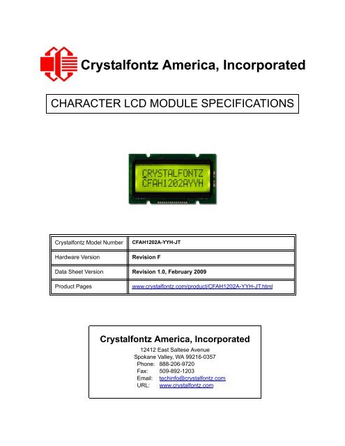
Crystalfontz America, IncorporatedCHARACTER <strong>LCD</strong> MODULE SPECIFICATIONSCrystalfontz Model NumberHardware VersionCFAH1202A-YYH-JTRevision FData Sheet Version Revision 1.0, February 2009Product Pageswww.crystalfontz.com/product/CFAH1202A-YYH-JT.htmlCrystalfontz America, Incorporated12412 East Saltese AvenueSpokane Valley, WA 99216-0357Phone: 888-206-9720Fax: 509-892-1203Email: techinfo@crystalfontz.comURL: www.crystalfontz.com
Crystalfontz America, Inc.CFAH1202A-YYH-JT Character <strong>LCD</strong> Module Data Sheetwww.crystalfontz.com Hardware vF / Data Sheet v1.0February 2009 Page 2REVISION HISTORYHARDWARE2009/02/05Current hardware version: vFThis “-JT” module replaces the discontinued “-JP” moduleCFAH1202A-YYH-JP.DATA SHEET2009/02/05Current Data Sheet version: v1.0New Data Sheet.The Fine PrintCertain applications using Crystalfontz America, Inc. products may involve potential risks of death, personal injury, or severeproperty or environmental damage (“Critical Applications”). CRYSTALFONTZ AMERICA, INC. PRODUCTS ARE NOTDESIGNED, INTENDED, AUTHORIZED, OR WARRANTED TO BE SUITABLE FOR USE IN LIFE-SUPPORTAPPLICATIONS, DEVICES OR SYSTEMS OR OTHER CRITICAL APPLICATIONS. Inclusion of Crystalfontz America, Inc.products in such applications is understood to be fully at the risk of the customer. In order to minimize risks associated withcustomer applications, adequate design and operating safeguards should be provided by the customer to minimize inherentor procedural hazard. Please contact us if you have any questions concerning potential risk applications.Crystalfontz America, Inc. assumes no liability for applications assistance, customer product design, software performance,or infringements of patents or services described herein. Nor does Crystalfontz America, Inc. warrant or represent that anylicense, either express or implied, is granted under any patent right, copyright, or other intellectual property right ofCrystalfontz America, Inc. covering or relating to any combination, machine, or process in which our products or servicesmight be or are used.The information in this publication is deemed accurate but is not guaranteed.Company and product names mentioned in this publication are trademarks or registered trademarks of their respectiveowners.Copyright © 2009 by Crystalfontz America, Inc., 12412 East Saltese Avenue, Spokane Valley, WA 99216-0357 U.S.A.
Crystalfontz America, Inc.CFAH1202A-YYH-JT Character <strong>LCD</strong> Module Data Sheetwww.crystalfontz.com Hardware vF / Data Sheet v1.0February 2009 Page 3CONTENTSMAIN FEATURES - - - - - - - - - - - - - - - - - - - - - - - - - - - - - - - - - - - - - - - - - - - - - - - - - - - - - - - - - - - - - - - - 4Module Classification Information - - - - - - - - - - - - - - - - - - - - - - - - - - - - - - - - - - - - - - - - - - - - - - - - - - - 4Ordering Information - - - - - - - - - - - - - - - - - - - - - - - - - - - - - - - - - - - - - - - - - - - - - - - - - - - - - - - - - - - - 5MECHANICAL SPECIFICATIONS - - - - - - - - - - - - - - - - - - - - - - - - - - - - - - - - - - - - - - - - - - - - - - - - - - - - 6Module Outline Drawing - - - - - - - - - - - - - - - - - - - - - - - - - - - - - - - - - - - - - - - - - - - - - - - - - - - - - - - - - 7ELECTRICAL SPECIFICATIONS - - - - - - - - - - - - - - - - - - - - - - - - - - - - - - - - - - - - - - - - - - - - - - - - - - - - - 8System Block Diagram - - - - - - - - - - - - - - - - - - - - - - - - - - - - - - - - - - - - - - - - - - - - - - - - - - - - - - - - - - 8Driving Method - - - - - - - - - - - - - - - - - - - - - - - - - - - - - - - - - - - - - - - - - - - - - - - - - - - - - - - - - - - - - - - - 9Absolute Maximum Ratings - - - - - - - - - - - - - - - - - - - - - - - - - - - - - - - - - - - - - - - - - - - - - - - - - - - - - - - 9DC Characteristics (5V and 3.3V Operation) - - - - - - - - - - - - - - - - - - - - - - - - - - - - - - - - - - - - - - - - - - 10Details of Interface Pin Functions - - - - - - - - - - - - - - - - - - - - - - - - - - - - - - - - - - - - - - - - - - - - - - - - - - 12Quick Reference for Pin Functions (Front & Back Photos) - - - - - - - - - - - - - - - - - - - - - - - - - - - - - - - - 13Typical V O Connections for Display Contrast - - - - - - - - - - - - - - - - - - - - - - - - - - - - - - - - - - - - - - - - - - 14ESD (Electro-Static Discharge) Specifications - - - - - - - - - - - - - - - - - - - - - - - - - - - - - - - - - - - - - - - - - 14OPTICAL SPECIFICATIONS - - - - - - - - - - - - - - - - - - - - - - - - - - - - - - - - - - - - - - - - - - - - - - - - - - - - - - - 15Optical Characteristics - - - - - - - - - - - - - - - - - - - - - - - - - - - - - - - - - - - - - - - - - - - - - - - - - - - - - - - - - - 15Optical Definitions - - - - - - - - - - - - - - - - - - - - - - - - - - - - - - - - - - - - - - - - - - - - - - - - - - - - - - - - - - - - - 15LED Backlight Characteristics - - - - - - - - - - - - - - - - - - - - - - - - - - - - - - - - - - - - - - - - - - - - - - - - - - - - 18<strong>LCD</strong> CONTROLLER INTERFACE - - - - - - - - - - - - - - - - - - - - - - - - - - - - - - - - - - - - - - - - - - - - - - - - - - - 21Display Position DDRAM Address - - - - - - - - - - - - - - - - - - - - - - - - - - - - - - - - - - - - - - - - - - - - - - - - -21Character Generator ROM (CGROM) - - - - - - - - - - - - - - - - - - - - - - - - - - - - - - - - - - - - - - - - - - - - - - - 22MODULE RELIABILITY AND LONGEVITY - - - - - - - - - - - - - - - - - - - - - - - - - - - - - - - - - - - - - - - - - - - - - 23Module Reliability - - - - - - - - - - - - - - - - - - - - - - - - - - - - - - - - - - - - - - - - - - - - - - - - - - - - - - - - - - - - - 23Module Longevity (EOL / Replacement Policy) - - - - - - - - - - - - - - - - - - - - - - - - - - - - - - - - - - - - - - - - 23CARE AND HANDLING PRECAUTIONS - - - - - - - - - - - - - - - - - - - - - - - - - - - - - - - - - - - - - - - - - - - - - - 24APPENDIX A: QUALITY ASSURANCE STANDARDS- - - - - - - - - - - - - - - - - - - - - - - - - - - - - - - - - - - - - 26APPENDIX B: APPLICATION NOTE FOR 3.3V OPERATION - - - - - - - - - - - - - - - - - - - - - - - - - - - - - - - 29APPENDIX C: SITRONIX ST7066U CONTROLLER SPECIFICATION SHEET - - - - - - - - - - - - - - - - - - - 31LIST OF FIGURESFigure 1. Module Outline Drawing - - - - - - - - - - - - - - - - - - - - - - - - - - - - - - - - - - - - - - - - - - - - - - - - - - - - 7Figure 2. System Block Diagram - - - - - - - - - - - - - - - - - - - - - - - - - - - - - - - - - - - - - - - - - - - - - - - - - - - - - 8Figure 3. Back View of Pins (Labeled) - - - - - - - - - - - - - - - - - - - - - - - - - - - - - - - - - - - - - - - - - - - - - - - - 13Figure 4. Front View of Pins (Labeled) - - - - - - - - - - - - - - - - - - - - - - - - - - - - - - - - - - - - - - - - - - - - - - - - 13Figure 5. Typical V O Connections - - - - - - - - - - - - - - - - - - - - - - - - - - - - - - - - - - - - - - - - - - - - - - - - - - - 14Figure 6. Definition of Operation Voltage (V OP ) (Positive)- - - - - - - - - - - - - - - - - - - - - - - - - - - - - - - - - - - 16Figure 7. Definition of Response Time (Tr, Tf) (Positive) - - - - - - - - - - - - - - - - - - - - - - - - - - - - - - - - - - - 16Figure 8. Definition of Horizontal and Vertical Viewing Angles (CR>2)- - - - - - - - - - - - - - - - - - - - - - - - - - 17Figure 9. Definition of 6:00 O’Clock and 12:00 O’Clock Viewing Angles - - - - - - - - - - - - - - - - - - - - - - - - 17Figure 10. Typical LED Backlight Connections for “Always On” - - - - - - - - - - - - - - - - - - - - - - - - - - - - - - - 18Figure 11. Example of LED Backlight Connections for PWM Dimming - - - - - - - - - - - - - - - - - - - - - - - - - - 20Figure 12. Character Generator ROM (CGROM) - - - - - - - - - - - - - - - - - - - - - - - - - - - - - - - - - - - - - - - - - 22
Crystalfontz America, Inc.CFAH1202A-YYH-JT Character <strong>LCD</strong> Module Data Sheetwww.crystalfontz.com Hardware vF / Data Sheet v1.0February 2009 Page 4MAIN FEATURES 12 characters by 2 lines <strong>LCD</strong> has a large display area in a compact 55.7 (W) x 32.0 (H) x 9.7 (D) millimeter package(2.19” (W) x 1.26” (H) x 0.38” (D)). 4-bit or 8-bit parallel interface. Standard Hitachi HD44780 equivalent controller. Yellow-green edge LED backlight with STN, positive, yellow-green, transflective mode <strong>LCD</strong> (displays dark characterson yellow-green background). Wide temperature operation: -20°C to +70°C. Direct sunlight readable. RoHS compliant.MODULE CLASSIFICATION INFORMATIONCFA H 12 02 A - Y Y H - J T * Brand Crystalfontz America, Inc. Display Type H – Character Number of Characters (Width) 12 Characters Number of Lines (Height) 2 Lines Model Identifier A Backlight Type & Color Y – LED, yellow-greenFluid Type, Image (Positive or Negative), & <strong>LCD</strong> GlassColorY – STN, positive, yellow-green Polarizer Film Type, Wide (WT) Temperature Range, & H – Transflective, WT, 6:00 1Viewing Angle (O'clock) Character Set (CGROM) J – English and Japanese fonts ControllerT – Sitronix ST7066U Special Codes* – May have additionalmanufacturer’s codes at thislocation.1 Note: For more information on Viewing Angle, see Definition of 6 O’Clock and 12:00 O’ClockViewing Angles (Pg. 17).
Crystalfontz America, Inc.CFAH1202A-YYH-JT Character <strong>LCD</strong> Module Data Sheetwww.crystalfontz.com Hardware vF / Data Sheet v1.0February 2009 Page 5ORDERING INFORMATIONPART NUMBERFLUID<strong>LCD</strong>GLASSCOLORIMAGEPOLARIZERFILMBACKLIGHTCOLOR/TYPECFAH1202A-YYH-JT STN yellow-green positive reflective yellow-green LEDAdditional variants (same form factor, different <strong>LCD</strong> mode or backlight):CFAH1202A-GGH-JT STN gray positive transflective green LEDCFAH1202A-NYG-JT STN yellow-green positive reflective no backlightCFAH1202A-TMI-JT STN blue negative transmissive white LEDCFAH1202A-TTI-JT FSTN near-black negative transmissive white LED
Crystalfontz America, Inc.CFAH1202A-YYH-JT Character <strong>LCD</strong> Module Data Sheetwww.crystalfontz.com Hardware vF / Data Sheet v1.0February 2009 Page 6MECHANICAL SPECIFICATIONSPHYSICAL CHARACTERISTICSITEMNumber of Characters and LinesModule DimensionsViewing AreaActive AreaCharacter SizeCharacter PitchDot SizeDot PitchWeightSIZE12 Characters x 2 Lines55.7 (W) x 32.0 (H) x 9.7 (D) mm46.0 (W) x 14.5 (H) mm37.85 (W) x 11.7 (H) mm2.65 (W) x 5.50 (H) mm3.20 (W) x 6.20 (H) mm0.45 (W) x 0.60 (H) mm0.55 (W) x 0.70 (H) mm16 grams (typical)
Crystalfontz America, Inc.CFAH1202A-YYH-JT Character <strong>LCD</strong> Module Data Sheetwww.crystalfontz.com Hardware vF / Data Sheet v1.0February 2009 Page 7MODULE OUTLINE DRAWING55.70±0.50 PCB51.30 Bezel46.70 Viewing Area37.85 Active Area31.20 PCB Mounting HolesSee PinDetail A5.109.70 MaximumKASee CharacterDetail C1 1517.78(P1.27 x 14)12.251.601.273.202.65.55.45.101.50.705.506.20.70.601.003.657.2510.15R1.50 TYPSee PinDetail B15-Ø0.7 PTH15-Ø1.0 PadSee DotDetail D11.4013.0014.5032.00±0.50 PCB24.70 Bezel17.50 BezelOpening14.50 VA11.70 AA2.204.504.858.9318.961.00.27.10.55Pin Detail APin Detail BCharacter Detail CDot Detail DNote: Tolerance is ±0.3 mm unless specified.copyright © 2008 by Part No.(s): CFAH1202A-YYH CFAH1202A-GGHScale:Not to scale Drawing Number:CFAH1202A_master Hardware Rev.:vFUnits:Date:Sheet:Millimeters2008/12/021 of 1Crystalfontz America, Inc.www.crystalfontz.com/products/Figure 1. Module Outline Drawing
Crystalfontz America, Inc.CFAH1202A-YYH-JT Character <strong>LCD</strong> Module Data Sheetwww.crystalfontz.com Hardware vF / Data Sheet v1.0February 2009 Page 8ELECTRICAL SPECIFICATIONSSYSTEM BLOCK DIAGRAMMPURSR/WEDB0-DB7HD44780EquivalentCom1-1612 x 2 <strong>LCD</strong>LEDBacklightAKVR10K-20KVDDVoVSSBias andPower CircuitSeg1-40Seg41-60Seg DriverFigure 2. System Block Diagram
Crystalfontz America, Inc.CFAH1202A-YYH-JT Character <strong>LCD</strong> Module Data Sheetwww.crystalfontz.com Hardware vF / Data Sheet v1.0February 2009 Page 9DRIVING METHODDRIVING METHODSPECIFICATIONDuty 1/16Bias 1/5ABSOLUTE MAXIMUM RATINGSABSOLUTE MAXIMUM RATINGSSYMBOLMINIMUMMAXIMUMOperating Temperature* T OP -20°C +70°CStorage Temperature* T ST -30°C +80°CInput Voltage V I V SS V DDSupply Voltage for Logic V DD - V SS -0.3v +7vSupply Voltage for <strong>LCD</strong> V DD - V O -0.3v +13v*Note: Prolonged exposure at temperatures outside of this range maycause permanent damage to the module.
Crystalfontz America, Inc.CFAH1202A-YYH-JT Character <strong>LCD</strong> Module Data Sheetwww.crystalfontz.com Hardware vF / Data Sheet v1.0February 2009 Page 10DC CHARACTERISTICS (5V AND 3.3V OPERATION)5V OPERATIONPARTDC CHARACTERISTICS(4.5 to 5.5 volts)TESTCONDITIONSYMBOLMINIMUMTYPICALMAXIMUMNOTESControllerandBoardSupply Voltage for Logic V DD - V SS +4.5v +5.0v +5.5vInput High Voltage V DD = 5V V IH +3.5v V DDPins: E, RS, R/W,DB0 - DB7Input Low Voltage V IL +0.6vOutput High Voltage V DD = 5V V OH +3.7vOutput Low Voltage V OL +0.4vI OH = - 0.1 mAPins: DB0 - DB7I OL = 0.1 mAPins: DB0 - DB7Supply CurrentwithoutbacklightI DD1.2 mA<strong>LCD</strong>GlassSupply Voltage forDriving <strong>LCD</strong>TA = -20ºCTA = +25ºC V DD - V O +3.8v+4.2vTA = +70ºC+3.6vThis is a summary of the module’s major operating parameters. For detailed information, see APPENDIX C:SITRONIX ST7066U CONTROLLER SPECIFICATION SHEET (Pg. 31).
Crystalfontz America, Inc.CFAH1202A-YYH-JT Character <strong>LCD</strong> Module Data Sheetwww.crystalfontz.com Hardware vF / Data Sheet v1.0February 2009 Page 113.3V OPERATIONPARTDC CHARACTERISTICS(2.7 to 4.5 volts)TESTCONDITIONSYMBOLMINIMUMTYPICALMAXIMUMNOTESControllerandBoardSupply Voltage for Logic V DD - V SS +2.7v +3.3v +4.5vInput High Voltage V DD = 3.3V V IH +2.3v V DDPins: E, RS, R/W,DB0 - DB7Input Low Voltage V IL +0.6vOutput High Voltage V DD = 3.3V V OH +2.4vOutput Low Voltage V OL +0.4vI OH = - 0.1 mAPins: DB0 - DB7I OL = 0.1 mAPins: DB0 - DB7Supply CurrentwithoutbacklightI DD1.2 mA<strong>LCD</strong>GlassSupply Voltage forDriving <strong>LCD</strong>TA = -20ºCTA = +25ºC V DD - V O +3.8vTA = +70ºC+3.6v+4.2vThis is a summary of the module’s major operating parameters. For detailed information see APPENDIX C:SITRONIX ST7066U CONTROLLER SPECIFICATION SHEET (Pg. 31).For more information about 3.3v operation, please see APPENDIX B: APPLICATION NOTE FOR 3.3VOPERATION (Pg. 29).
Crystalfontz America, Inc.CFAH1202A-YYH-JT Character <strong>LCD</strong> Module Data Sheetwww.crystalfontz.com Hardware vF / Data Sheet v1.0February 2009 Page 12DETAILS OF INTERFACE PIN FUNCTIONSPIN SIGNAL LEVELDIRECTIONDESCRIPTION1 V SS 0v Ground2 V DD +5.0v Supply voltage for logic3 V O variable4 RS H/L I5 R/W H/L I6 E H,HL ISupply voltage for driving <strong>LCD</strong> is V O = +1v typical at V DD = +5vwhich gives a V <strong>LCD</strong> = (V DD - V O ) = +4vRegister selection inputH: Data register (for read and write) L: Instruction code (for write)H: Read (MPUModule)L: Write (MPUModule)Read/write enable signalH: Read data is enabled by a high levelHL: Write data is latched on the falling edge7 DB0 H/L I/O Data bit 08 DB1 H/L I/O Data bit 19 DB2 H/L I/O Data bit 210 DB3 H/L I/O Data bit 311 DB4 H/L I/O Data bit 412 DB5 H/L I/O Data bit 513 DB6 H/L I/O Data bit 614 DB7 H/L I/O Data bit 715 A (LED +)Supply voltage for LED. “A” (anode) or “+” of LED backlightPlease Note: "K" (cathode) or "-" of LED backlight is internally connected toV DDFor backlight connections, please refer to LED Backlight Characteristics (Pg. 18).
Crystalfontz America, Inc.CFAH1202A-YYH-JT Character <strong>LCD</strong> Module Data Sheetwww.crystalfontz.com Hardware vF / Data Sheet v1.0February 2009 Page 13QUICK REFERENCE FOR PIN FUNCTIONS (FRONT & BACK PHOTOS)(1) V SS(3) V O(5) R/W(7) DB0(9) DB2(11) DB4(13) DB6(15) A (LED +)(2) V DD(4) RS(6) E(8) DB1(10) DB3(12) DB5(14) DB7Figure 3. Back View of Pins (Labeled)(15) A (LED +)(13) DB6(11) DB4(9) DB2(7) DB0(5) R/W(3) V O(1) V SS(14) DB7(12) DB5(10) DB3(8) DB1(6) E(4) RS(2) V DDFigure 4. Front View of Pins (Labeled)
Crystalfontz America, Inc.CFAH1202A-YYH-JT Character <strong>LCD</strong> Module Data Sheetwww.crystalfontz.com Hardware vF / Data Sheet v1.0February 2009 Page 14TYPICAL V O CONNECTIONS FOR DISPLAY CONTRASTAdjust V O to +1v (V <strong>LCD</strong> = +4v) as an initial setting. When the module is operational, readjust V O for optimal displayappearance.V DDV <strong>LCD</strong>VR10 kV OV SS(Ground)V SSFigure 5. Typical V O ConnectionsWe recommend allowing field adjustment of V O for all designs. The optimal value for V O will change with temperature,variations in V DD , and viewing angle. V O will also vary module-to-module and batch-to-batch due to normalmanufacturing variations.Ideally, adjustments to V O should be available to the end user so each user can adjust the display to the optimal contrastfor their required viewing conditions. At a minimum, your design should allow V O to be adjusted as part of your product’sfinal test.Although a potentiometer is shown as a typical connection, V O can be driven by your microcontroller, either by using aDAC or a filtered PWM. Displays that require V O to be negative may need a level-shifting circuit. Please do not hesitateto contact Crystalfontz application support for design assistance on your application.ESD (ELECTRO-STATIC DISCHARGE) SPECIFICATIONSThis circuitry is industry standard CMOS logic and is susceptible to ESD damage. Please use industry standard antistaticprecautions as you would for any other PCB such as expansion cards or motherboards. For more information, see CAREAND HANDLING PRECAUTIONS (Pg. 24).
Crystalfontz America, Inc.CFAH1202A-YYH-JT Character <strong>LCD</strong> Module Data Sheetwww.crystalfontz.com Hardware vF / Data Sheet v1.0February 2009 Page 15OPTICAL SPECIFICATIONSOPTICAL CHARACTERISTICSITEMSYMBOLCONDITIONMINIMUMTYPICALMAXIMUMViewing Angle (6 o’clock)(Vertical, Horizontal)(V) CR>2 20° 40°(H) CR>2 -30° 30°Contrast Ratio CR 3<strong>LCD</strong> Response Time* T rise Ta = 25°C 150 ms 200 msT fall Ta = 25°C 150 ms 200 ms*Response Time: The amount of time it takes a liquid crystal cell to go fromactive to inactive or back again.OPTICAL DEFINITIONS• Operating Voltage (V <strong>LCD</strong> ): V OP• Viewing Angle• Vertical (V): 0°• Horizontal (H): 0°• Frame Frequency: 64 Hz• Driving Waveform: 1/16 Duty, 1/5 Bias• Ambient Temperature (Ta): 25°C
Crystalfontz America, Inc.CFAH1202A-YYH-JT Character <strong>LCD</strong> Module Data Sheetwww.crystalfontz.com Hardware vF / Data Sheet v1.0February 2009 Page 16Definition of Operation Voltage (Vop)Intensity100%Selected WaveNon-selected WaveCRMaximumCR = L on/ L offL on =Luminance of ON segmentsL off =Luminance of OFF segmentsV opDriving Voltage (V)Figure 6. Definition of Operation Voltage (V OP ) (Positive)Definition of Response Time (Tr, Tf)UnselectedStateSelectedStateUnselectedStateLightTransmitted10%Intensity100%90%LightBlockedTrTr = Rise TimeTf = Fall TimeTfFigure 7. Definition of Response Time (Tr, Tf) (Positive)
Crystalfontz America, Inc.CFAH1202A-YYH-JT Character <strong>LCD</strong> Module Data Sheetwww.crystalfontz.com Hardware vF / Data Sheet v1.0February 2009 Page 17Definition of Vertical and Horizontal Viewing Angles (CR>2)VerticalHorizontalFigure 8. Definition of Horizontal and Vertical Viewing Angles (CR>2)Definition of 6 O’Clock and 12:00 O’Clock Viewing AnglesThis module has a 6:00 o’clock viewing angle. A 6:00 o’clock viewing angle is a bottom viewing angle like what you wouldsee when you look at a cell phone or calculator. A 12:00 o’clock viewing angle is a top viewing angle like what you wouldsee when you look at the gauges in a golf cart or airplane.Eyes look downEyes look up6:00 O’clockBottom Viewing Angle12:00 O’clockTop Viewing AngleFigure 9. Definition of 6:00 O’Clock and 12:00 O’Clock Viewing Angles
Crystalfontz America, Inc.CFAH1202A-YYH-JT Character <strong>LCD</strong> Module Data Sheetwww.crystalfontz.com Hardware vF / Data Sheet v1.0February 2009 Page 18LED BACKLIGHT CHARACTERISTICSThe CFAH1202A-YYH-JT uses an LED backlight. LED backlights are easy to use, but they are also easily damaged byabuse.NOTEDo not connect +5v directly to the backlight terminals. This will ruin thebacklight.LEDs are “current” devices. The important aspect of driving an LED is the current flowing through it, not the voltageacross it. Ideally, a current source would be used to drive the LEDs. In practice, a simple current limiting resistor in linefrom a voltage source will work well in most applications and is much less complex than a current source.You need to know what the forward voltage of the LEDs is so you can calculate the current limiting resistor (R LIMIT ). Theforward voltage will vary slightly from display to display.15 1V DDAnodeGNDFigure 10. Typical LED Backlight Connections for “Always On”
Crystalfontz America, Inc.CFAH1202A-YYH-JT Character <strong>LCD</strong> Module Data Sheetwww.crystalfontz.com Hardware vF / Data Sheet v1.0February 2009 Page 19How to Calculate the R LIMITThe equation to calculate R LIMIT is:R LIMIT (minimum) =V DD (Supply Voltage) - V LED (Typical LED Forward Voltage)I LED (Typical LED Forward Current)The specific R LIMIT calculation for the CFAH1202A-YYH-JT at V DD = +5v is:R LIMIT =5v - 4.2v0.04 A= 20.0Ω (minimum)How to Calculate the Power Rating of the ResistorThe general equation to calculate the power rating of the resistor is:W (power) = 1 (current) x E (voltage)The specific power rating calculation for the CFAH1202A-YYH-JT is:Power = 0.04A x (5v - 4.2v) = 0.032W = 32mWNominally, an 1/8 watt (125 mW) resistor should work, however in order to keep the temprature of the resistor cooler a1/4 or 1/2 watt resistor would typically be used.
Crystalfontz America, Inc.CFAH1202A-YYH-JT Character <strong>LCD</strong> Module Data Sheetwww.crystalfontz.com Hardware vF / Data Sheet v1.0February 2009 Page 20PWM DimmingThe backlight may be dimmed by PWM (Pulse Width Modulation). The typical range for the PWM frequency is from 100to 300 Hz.15 1OnPWM signalfrommicrocontrollerOff1K V DDR LIMITP-Type FETIRLML6402(typical)AnodeGNDFigure 11. Example of LED Backlight Connections for PWM Dimming
Crystalfontz America, Inc.CFAH1202A-YYH-JT Character <strong>LCD</strong> Module Data Sheetwww.crystalfontz.com Hardware vF / Data Sheet v1.0February 2009 Page 21Backlight Characteristicsdark dots on yellow-green backgroundPARAMETER MINIMUM TYPICAL MAXIMUMForward Current (I LED)V = 4.2v32 mA 40 mA 60 mAForward Voltage (V LED ) +4.0v +4.2v +4.4vReverse Voltage (V R ) +8vLuminous Intensity* (I V )I LED = 40 mAWavelength* (l )I LED = 40 mA10 cd/m 2 27 cd/m 2 40 cd/m 2573 nm*Direct measurement of backlight–the backlight is not measured through the <strong>LCD</strong>.<strong>LCD</strong> CONTROLLER INTERFACEThis module uses a Sitronix ST7066U controller. The Sitronix ST7066U is compatible with the industry standard HitachiHD44780 controller. Software written for modules that use the HD44780 should work without modification.For your reference, we added APPENDIX C: SITRONIX ST7066U CONTROLLER SPECIFICATION SHEET (Pg. 31) tothis Data Sheet.DISPLAY POSITION DDRAM ADDRESSThe following table shows the relationship between the controller’s addresses and the corresponding character locationon the module.COLUMN1 2 3 4 5 6 7 8 9 10 11 120 0x00 0x01 0x02 0x03 0x04 0x05 0x06 0x07 0x08 0x09 0xAROW 0xB1 0x40 0x41 0x42 0x43 0x44 0x45 0x46 0x47 0x48 0x49 0x4A 0x4B
Crystalfontz America, Inc.CFAH1202A-YYH-JT Character <strong>LCD</strong> Module Data Sheetwww.crystalfontz.com Hardware vF / Data Sheet v1.0February 2009 Page 22CHARACTER GENERATOR ROM (CGROM)To find the code for a given character, add the two numbers that are shown in bold for its row and column. For example,the lowercase “h” is in the column labeled “96 10 ” and in the row labeled “8 10 ”. So you would add 96 + 8 to get 104. Whenyou send a byte with the value of 104 to the display, then a lowercase “h” will be shown. (See APPENDIX C: SITRONIXST7066U CONTROLLER SPECIFICATION SHEET (Pg. 31).upper4 bits 0 1016lower1032 1048 1064 1080 1096 10112 10128 10144 10160 10176 10192 10208 10224 10240 1000004 bits20001 20010 20011 20100 20101 20110 20111 21000 20001 20010 20011 21100 21101 21110 21111 20 100000 2CGRAM[0]1 100001 2CGRAM[1]2 100010 2CGRAM[2]3 100011 2CGRAM[3]4 100100 2CGRAM[4]5 100101 2CGRAM[5]6 100110 2CGRAM[6]7 100111 2CGRAM[7]8 101000 29 101001 210 101010 211 101011 <strong>212</strong> 101100 213 101101 214 101110 2015 101111 2Figure 12. Character Generator ROM (CGROM)
Crystalfontz America, Inc.CFAH1202A-YYH-JT Character <strong>LCD</strong> Module Data Sheetwww.crystalfontz.com Hardware vF / Data Sheet v1.0February 2009 Page 23MODULE RELIABILITY AND LONGEVITYMODULE RELIABILITYITEM<strong>LCD</strong> including yellow-green LED backlightSPECIFICATION50,000 to 100,000 hours (typical)MODULE LONGEVITY (EOL / REPLACEMENT POLICY)Crystalfontz is committed to making all of our <strong>LCD</strong> modules available for as long as possible. For each module weintroduce, we intend to offer it indefinitely. We do not preplan a module's obsolescence. The majority of modules we haveintroduced are still available.We recognize that discontinuing a module may cause problems for some customers. However, rapidly changingtechnologies, component availability, or low customer order levels may force us to discontinue (“End of Life”, EOL) amodule. For example, we must occasionally discontinue a module when a supplier discontinues a component or amanufacturing process becomes obsolete. When we discontinue a module, we will do our best to find an acceptablereplacement module with the same fit, form, and function.In most situations, you will not notice a difference when comparing a “fit, form, and function” replacement module to thediscontinued module it replaces. However, sometimes a change in component or process for the replacement moduleresults in a slight variation, perhaps an improvement, over the previous design.Although the replacement module is still within the stated Data Sheet specifications and tolerances of the discontinuedmodule, changes may require modification to your circuit and/or firmware. Possible changes include:• <strong>LCD</strong> fluid, polarizers, or the <strong>LCD</strong> manufacturing process. These items may change the appearance of thedisplay, requiring an adjustment to V O (See Typical V O Connections for Display Contrast (Pg. 14)).• Backlight LEDs. Brightness may be affected (perhaps the new LEDs have better efficiency) or the current theydraw may change (new LEDs may have a different VF).• Controller. A new controller may require minor changes in your code.• Component tolerances. Module components have manufacturing tolerances. In extreme cases, the tolerancestack can change the visual or operating characteristics.Please understand that we avoid changing a module whenever possible; we only discontinue a module if we have noother option. We will post Part Change Notices on the product's webpage as soon as possible. If interested, you cansubscribe to future part change notifications.
Crystalfontz America, Inc.CFAH1202A-YYH-JT Character <strong>LCD</strong> Module Data Sheetwww.crystalfontz.com Hardware vF / Data Sheet v1.0February 2009 Page 24CARE AND HANDLING PRECAUTIONSFor optimum operation of the module and to prolong its life, please follow the precautions below.ESD (ELECTRO-STATIC DISCHARGE)The circuitry is industry standard CMOS logic and susceptible to ESD damage. Please use industry standard antistaticprecautions as you would for any other PCB such as expansion cards or motherboards. Ground your body, worksurfaces, and equipment.DESIGN AND MOUNTING• The exposed surface of the <strong>LCD</strong> “glass” is actually a polarizer laminated on top of the glass.To protect the softplastic polarizer from damage, the module ships with a protective film over the polarizer. Please peel off theprotective film slowly. Peeling off the protective film abruptly may generate static electricity.• The polarizer is made out of soft plastic and is easily scratched or damaged. When handling the module, avoidtouching the polarizer. Finger oils are difficult to remove.• To protect the soft plastic polarizer from damage, place a transparent plate (for example, acrylic, polycarbonate,or glass) in front of the module, leaving a small gap between the plate and the display surface. We use GE HP-92 Lexan, which is readily available and works well.• Do not disassemble or modify the module.• Do not modify the tab of the metal holder or make connections to it.• Solder only to the I/O terminals. Use care when removing solder—it is possible to damage the PCB.• Do not reverse polarity to the power supply connections. Reversing polarity will immediately ruin the module.AVOID SHOCK, IMPACT, TORQUE, AND TENSION• Do not expose the module to strong mechanical shock, impact, torque, and tension.• Do not drop, toss, bend, or twist the module.• Do not place weight or pressure on the module.IF <strong>LCD</strong> PANEL BREAKS• If the <strong>LCD</strong> panel breaks, be careful not to get the liquid crystal fluid in your mouth or eyes.• If the liquid crystal fluid touches your skin, clothes, or work surface, wash it off immediately using soap and plentyof water.• Do not eat the <strong>LCD</strong> panel.CLEANINGThe polarizer (laminated to the glass) is soft plastic. The soft plastic is easily scratched or damaged. Be very carefulwhen you clean the polarizer.• Do not clean the polarizer with liquids. Do not wipe the polarizer with any type of cloth or swab (for example, Q-tips).• Use the removable protective film to remove smudges (for example, fingerprints) and any foreign matter. If youno longer have the protective film, use standard transparent office tape (for example, Scotch® brand “CrystalClear Tape”). If the polarizer is dusty, you may carefully blow it off with clean, dry, oil-free compressed air.
Crystalfontz America, Inc.CFAH1202A-YYH-JT Character <strong>LCD</strong> Module Data Sheetwww.crystalfontz.com Hardware vF / Data Sheet v1.0February 2009 Page 25OPERATION• We do not recommend connecting this module to a PC's parallel port as an "end product.” This module is not"user friendly" and connecting them to a PC's parallel port is often difficult, frustrating, and can result in a "dead"display due to mishandling. For more information, see our forum thread at http://www.crystalfontz.com/forum/showthread.php?s=&threadid=3257.• Your circuit should be designed to protect the module from ESD and power supply transients.• Observe the operating temperature limitations: from -20°C minimum to +70°C maximum with minimalfluctuations. Operation outside of these limits may shorten the life and/or harm the display.• At lower temperatures of this range, response time is delayed.• At higher temperatures of this range, display becomes dark. (You may need to adjust the contrast.)• Operate away from dust, moisture, and direct sunlight.STORAGE AND RECYCLING• Store in an ESD-approved container away from dust, moisture, and direct sunlight.• Observe the storage temperature limitations: from -30°C minimum to +80°C maximum with minimal fluctuations.Rapid temperature changes can cause moisture to form, resulting in permanent damage.• Do not allow weight to be placed on the modules while they are in storage.• Please recycle your outdated Crystalfontz <strong>LCD</strong> modules at an approved facility.
Crystalfontz America, Inc.CFAH1202A-YYH-JT Character <strong>LCD</strong> Module Data Sheetwww.crystalfontz.com Hardware vF / Data Sheet v1.0February 2009 Page 26APPENDIX A: QUALITY ASSURANCE STANDARDSINSPECTION CONDITIONS• Environment• Temperature: 25±5°C• Humidity: 30~85% RH (noncondensing)• For visual inspection of active display area• Source lighting: two 20-Watt or one 40-Watt fluorescent light• Display adjusted for best contrast• Viewing distance: 30±5 cm (about 12 inches)• Viewing angle: inspect at 45° angle of vertical line right and left, top and bottomCOLOR DEFINITIONSWe try to describe the appearance of our <strong>LCD</strong> modules as accurately as possible. For the photos, we adjust the backlight(if any) and contrast for optimal appearance. Actual display appearance may vary due to (1) different operatingconditions, (2) small variations of component tolerances, (3) inaccuracies of our camera, (4) color interpretation of thephotos on your monitor, and/or (5) personal differences in the perception of color.DEFINITION OF ACTIVE AREA AND VIEWING AREA46.70 Viewing Area37.85 Active Area14.5 VA11.70 AAACCEPTANCE SAMPLINGDEFECT TYPE AQL*Major
Crystalfontz America, Inc.CFAH1202A-YYH-JT Character <strong>LCD</strong> Module Data Sheetwww.crystalfontz.com Hardware vF / Data Sheet v1.0February 2009 Page 27DEFECTS CLASSIFICATIONDefects are defined as:• Major Defect: results in failure or substantially reduces usability of unit for its intended purpose• Minor Defect: deviates from standards but is not likely to reduce usability for its intended purposeACCEPTANCE STANDARDS# DEFECT TYPE CRITERIA1 Electrical defects 1. No display, display malfunctions, or shorted segments.2. Current consumption exceeds specifications.MAJOR /MINORMajor2 Viewing area defect Viewing area does not meet specifications. Major3 Contrast adjustmentdefectContrast adjustment fails or malfunctions.Major4 Blemishes or foreignmatter on displaysegmentsBlemishDefect Size Acceptable Qty
Crystalfontz America, Inc.CFAH1202A-YYH-JT Character <strong>LCD</strong> Module Data Sheetwww.crystalfontz.com Hardware vF / Data Sheet v1.0February 2009 Page 28# DEFECT TYPE CRITERIAMAJOR /MINOR7 Bubbles between polarizer film and glass Defect Size Acceptable Qty0.60 mm 08 Display pattern defectDAEGFDot SizeBCAcceptable QtyMinor((A+B)/2)0 mm((D+E)/2)
Crystalfontz America, Inc.CFAH1202A-YYH-JT Character <strong>LCD</strong> Module Data Sheetwww.crystalfontz.com Hardware vF / Data Sheet v1.0February 2009 Page 29APPENDIX B: APPLICATION NOTE FOR 3.3V OPERATIONThis module can be used with a 3.3v power supply. In order to meet the requirements of V <strong>LCD</strong> , you must provide anegative voltage source for V O (pin 3, see Details of Interface Pin Functions (Pg. 12)). You need to drive V O to belowground (typically -1v or -2v) until the V <strong>LCD</strong> is met, making display contrast acceptable.You can supply the negative voltage by one of the following methods:1. Use an available source for the negative voltage.V SS 3.3v10K typicalV O-1.2vExistingNegativeVoltage Supply(-3v to -15v)**Optional resistor to limit the voltage seen by themodule at V O to within specifications.Figure 1. Use Existing Negative Voltage Supply2. Use a “7660” CMOS switched-capacitor voltage converter or one of the many other available solutions forcreating a negative voltage from a positive supply.3.3v10K typical V O -1.2v3.3v“7660”-3.3vV SSFigure 2. “7660” Switched-Capacitor Voltage Converter
Crystalfontz America, Inc.CFAH1202A-YYH-JT Character <strong>LCD</strong> Module Data Sheetwww.crystalfontz.com Hardware vF / Data Sheet v1.0February 2009 Page 303. Use the circuit in the figure below to create the voltage for V O by using a PWM (Pulse Width Modulation) outputof your microcontroller. This circuit allows the contrast to be adjusted under software control.PWM(7 to 10 kHz typical)1K0.1μFLow V fSchottkyV OLow V fSchottkyC60.1μFGNDGNDFigure 3. V O Driving CircuitSince V O is pulled up internally by the <strong>LCD</strong> controller, this circuit will produce positive (+1v) V <strong>LCD</strong> (V <strong>LCD</strong> = small,contrast is light) for low (10%) or high (90%) duty cycles. For duty cycles near 50%, this circuit will produce negative(-2v) levels of V O (V <strong>LCD</strong> = big, contrast is dark).4. Replace this module with the module in this series that has an on-board negative voltage generator. (The partnumber has a “V” at the end of it.)3.3v = V DD “-V” <strong>LCD</strong>Module10K typicalV O (Pin 3)V EE (Pin 15)-3.3v outFigure 4. On-Board Negative Voltage Generator
Crystalfontz America, Inc.CFAH1202A-YYH-JT Character <strong>LCD</strong> Module Data Sheetwww.crystalfontz.com Hardware vF / Data Sheet v1.0February 2009 Page 31APPENDIX C: SITRONIX ST7066U CONTROLLERSPECIFICATION SHEETThe complete Sitronix ST7066U Dot Matrix <strong>LCD</strong> Controller/Driver specifications (42 pages) follows.
STSitronixST7066UDot Matrix <strong>LCD</strong> Controller/Driver• Features• 5 x 8 and 5 x 11 dot matrix possible• Low power operation support:-- 2.7 to 5.5V• Wide range of <strong>LCD</strong> driver power-- 3.0 to 10V• Correspond to high speed MPU businterface-- 2 MHz (when VCC = 5V)• 4-bit or 8-bit MPU interface enabled• 80 x 8-bit display RAM (80 characters max.)• 13,200-bit character generator ROM for atotal of 240 character fonts(5 x 8 dot or 5 x 11dot)• 64 x 8-bit character generator RAM-- 8 character fonts (5 x 8 dot)-- 4 character fonts (5 x 11 dot)• DescriptionThe ST7066U dot-matrix liquid crystal displaycontroller and driver LSI displays alphanumeric,Japanese kana characters, and symbols. It can beconfigured to drive a dot-matrix liquid crystal displayunder the control of a 4- or 8-bit microprocessor.Since all the functions such as display RAM,character generator, and liquid crystal driver, requiredfor driving a dot-matrix liquid crystal display areinternally provided on one chip, a minimal system canbe interfaced with this controller/driver.The ST7066U character generator ROM is extendedto generate 240 5x8(5x11) dot character fonts for a• 16-common x 40-segment liquid crystaldisplay driver• Programmable duty cycles-- 1/8 for one line of 5 x 8 dots with cursor-- 1/11 for one line of 5 x 11 dots & cursor-- 1/16 for two lines of 5 x 8 dots & cursor• Wide range of instruction functions:Display clear, cursor home, display on/off,cursor on/off, display character blink, cursorshift, display shift• Automatic reset circuit that initializes thecontroller/driver after power on• Internal oscillator with external resistors• Low power consumption• QFP80 and Bare Chip availabletotal of 240 different character fonts. The low powersupply (2.7V to 5.5V) of the ST7066U is suitable forany portable battery-driven product requiring lowpower dissipation.The ST7066U <strong>LCD</strong> driver consists of 16 commonsignal drivers and 40 segment signal drivers whichcan extend display size by cascading segment driverST7065 or ST7063. The maximum display size canbe either 80 characters in 1-line display or 40characters in 2-line display. A single ST7066U candisplay up to one 8-character line or two 8-characterlines.Product NameST7066U-0AST7066U-0BST7066U-0ESupport CharacterEnglish / JapanEnglish / EuropeanEnglish / EuropeanAppendixV2.2 1/42 2006/05/11
ST7066UST7066 Serial Specification Revision HistoryVersion Date Description1.7 2000/10/311. Added 8051 Example Program Code(Page 21,23)2. Added Annotated Flow Chart :“BF cannot be checked before this instruction”3. Changed Maximum RatingsPower Supply Voltage:+5.5V →+7.0V(Page 28)1.8 2000/11/14 Added QFP Pad Configuration(Page 5)1.8a 2000/11/301. Moved QFP Package Dimensions(Page 39) toPage 52. Changed DC Characteristics Ratings(Page32,33)2.0 2001/03/01 Transition to ST7066U2.1 2006/04/101. Add Power Supply Conditions (Page 31);2. Modify reset description on Page 22.2.2 2006/05/11 Emphasis checking BF procedure (Page 9, 27, 28).AppendixV2.2 2/42 2006/05/11
ST7066U• Block DiagramResetcircuitOSC1 OSC2CPGTiminggeneratorCL1CL2MInstructionregister(IR)DRSRWEMPUinterfaceInstructiondecoderDisplay dataRAM(DDRAM)80x8 bits16-bitshiftregisterCommonsignaldriverCOM1 toCOM16Addresscounter40-bitshiftregister40-bitlatchcircuitSegmentsignaldriverSEG1 toSEG40DB4 toDB7Dataregister(DR)DB0 toDB3Input/outputbufferBusyflag<strong>LCD</strong> drivevoltageselectorCharactergeneratorRAM(CGRAM)64 bytesCharactergeneratorROM(CGROM)13,200 bitsCursorandblinkcontrollerGNDParallel/serial converterandattribute circuitVccV1 V2 V3 V4 V5AppendixV2.2 3/42 2006/05/11
ST7066U• Pad ArrangementSEG221 80 79 78 77 76 75 74 73 72 71 70 69 68 67 66 65 64SEG39SEG21SEG2023ST7066U6362SEG40COM16SEG19461COM15SEG18560COM14SEG17659COM13SEG16758COM12SEG15857COM11SEG149(0,0)56COM10SEG131055COM09SEG121154COM08SEG11SEG10SEG09SEG0812131415Chip Size : 2300x3000μmCoordinate : Pad CenterOrigin : Chip CenterMin Pad Pitch : 120μmPad Size : 96x96μm53525150COM07COM06COM05COM04SEG071649SEG061748SEG051847SEG041946DB7SEG032045DB6SEG022144DB5SEG012243DB4GND2342DB3OSC124 25 26 27 28 29 30 31 32 33 3 35 36 37 38 39 40 41DB2OSC2V1V2V3V4V5CL1CL2VccMDRSR/WEDB0DB1SEG23SEG24SEG25SEG26SEG27SEG28SEG29SEG30SEG31SEG32SEG33SEG34SEG35SEG36SEG37SEG38COM03COM02COM01Substrate Connect to VDD.AppendixV2.2 4/42 2006/05/11
ST7066U• Package DimensionsAppendixV2.2 5/42 2006/05/11
ST7066UV2.2 6/42 2006/05/11• Pad Configuration(80 QFP)25262728293031323334353637383940OSC2V1V2V3V4V5CL1CL2VCCM D RSRWEDB0DB180797877767574737271706968676665S23S24S25S26S27S28S29S30S31S32S33S34S35S36S37S38S22S21S20S19S18S17S16S15S14S13S12S11S10S09S08S07S06S05S04S03S02S01GNDOSC1S39S40C16C15C14C13C12C11C10C09C08C07C06C05C04C03C02C01DB7DB6DB5DB4DB2DB31234567891011121314151617181920<strong>212</strong>22324646362616059585756555453525150494847464544434241Appendix
ST7066U• Pad Location CoordinatesPad No. Function X Y Pad No. Function X Y1 SEG22 -1040 1400 41 DB2 1040 -14002 SEG21 -1040 1270 42 DB3 1040 -12703 SEG20 -1040 1140 43 DB4 1040 -11404 SEG19 -1040 1020 44 DB5 1040 -10205 SEG18 -1040 900 45 DB6 1040 -9006 SEG17 -1040 780 46 DB7 1040 -7807 SEG16 -1040 660 47 COM1 1040 -6608 SEG15 -1040 540 48 COM2 1040 -5409 SEG14 -1040 420 49 COM3 1040 -42010 SEG13 -1040 300 50 COM4 1040 -30011 SEG12 -1040 180 51 COM5 1040 -18012 SEG11 -1040 60 52 COM6 1040 -6013 SEG10 -1040 -60 53 COM7 1040 6014 SEG9 -1040 -180 54 COM8 1040 18015 SEG8 -1040 -300 55 COM9 1040 30016 SEG7 -1040 -420 56 COM10 1040 42017 SEG6 -1040 -540 57 COM11 1040 54018 SEG5 -1040 -660 58 COM12 1040 66019 SEG4 -1040 -780 59 COM13 1040 78020 SEG3 -1040 -900 60 COM14 1040 90021 SEG2 -1040 -1020 61 COM15 1040 102022 SEG1 -1040 -1140 62 COM16 1040 114023 GND -1040 -1270 63 SEG40 1040 127024 OSC1 -1040 -1400 64 SEG39 1040 140025 OSC2 -910 -1400 65 SEG38 910 140026 V1 -780 -1400 66 SEG37 780 140027 V2 -660 -1400 67 SEG36 660 140028 V3 -540 -1400 68 SEG35 540 140029 V4 -420 -1400 69 SEG34 420 140030 V5 -300 -1400 70 SEG33 300 140031 CL1 -180 -1400 71 SEG32 180 140032 CL2 -60 -1400 72 SEG31 60 140033 Vcc 60 -1400 73 SEG30 -60 140034 M 180 -1400 74 SEG29 -180 140035 D 300 -1400 75 SEG28 -300 140036 RS 420 -1400 76 SEG27 -420 140037 RW 540 -1400 77 SEG26 -540 140038 E 660 -1400 78 SEG25 -660 140039 DB0 780 -1400 79 SEG24 -780 140040 DB1 910 -1400 80 SEG23 -910 1400AppendixV2.2 7/42 2006/05/11
ST7066U• Pin FunctionName Number I/O Interfaced with FunctionRS 1 I MPUSelect registers.0: Instruction register (for write) Busy flag:address counter (for read)1: Data register (for write and read)R/W 1 I MPUSelect read or write.0: Write1: ReadE 1 I MPU Starts data read/write.DB4 to DB7 4 I/O MPUFour high order bi-directional tristate data buspins. Used for data transfer and receivebetween the MPU and the ST7066U. DB7 canbe used as a busy flag.DB0 to DB3 4 I/O MPUFour low order bi-directional tristate data buspins. Used for data transfer and receivebetween the MPU and the ST7066U.These pins are not used during 4-bit operation.CL1 1 O Extension driverClock to latch serial data D sent to theextension driverCL2 1 O Extension driver Clock to shift serial data DM 1 O Extension driverSwitch signal for converting the liquid crystaldrive waveform to ACD 1 O Extension driverCharacter pattern data corresponding to eachCOM1 toCOM16SEG1 toSEG4016 O <strong>LCD</strong>40 O <strong>LCD</strong>V1 to V5 5 - Power supplysegment signalCommon signals that are not used are changedto non-selection waveform. COM9 to COM16are non-selection waveforms at 1/8 duty factorand COM12 to COM16 are non-selectionwaveforms at 1/11 duty factor.Segment signalsPower supply for <strong>LCD</strong> driveVCC - V5 = 10 V (Max)VCC , GND 2 - Power supply VCC : 2.7V to 5.5V, GND: 0VOSC1, OSC2 2Oscillationresistor clockNote:1. Vcc>=V1>=V2>=V3>=V4>=V5 must be maintained2. Two clock options:When crystal oscillation is performed, a resistormust be connected externally. When the pininput is an external clock, it must be input to OSC1.R=91KΩ (Vcc=5V)R=75KΩ (Vcc=3V)OSC1 OSC2 OSC1 OSC2RClock inputAppendixV2.2 8/42 2006/05/11
ST7066U• Function Description• System InterfaceThis chip has all two kinds of interface type with MPU : 4-bit bus and 8-bit bus. 4-bit bus or 8-bit bus is selectedby DL bit in the instruction register.During read or write operation, two 8-bit registers are used. One is data register (DR), the other is instructionregister(IR).The data register(DR) is used as temporary data storage place for being written into or read fromDDRAM/CGRAM, target RAM is selected by RAM address setting instruction. Each internal operation, readingfrom or writing into RAM, is done automatically. So to speak, after MPU reads DR data, the data in the nextDDRAM/CGRAM address is transferred into DR automatically. Also after MPU writes data to DR, the data in DRis transferred into DDRAM/CGRAM automatically.The Instruction register(IR) is used only to store instruction code transferred from MPU. MPU cannot use it toread instruction data.To select register, use RS input pin in 4-bit/8-bit bus mode.RS R/WLLHHOperationInstructionWriteoperation (MPUwritesInstructioncodeLinto IR)H Read Busy Flag(DB7) and address counter (DB0 ~ DB6)L Data Write operation (MPU writes data into DR)H Data Read operation (MPU reads data from DR)Table 1. Various kinds of operations according to RS and R/W bits.• Busy Flag (BF)When BF = "High”, it indicates that the internal operation is being processed. So during this time the nextinstruction cannot be accepted. BF can be read, when RS = Low and R/W = High (Read Instruction Operation),through DB7 port. Before executing the next instruction, be sure that BF is not High. Before checking BF, besure to wait at least 80us. Please refer to Page 27 for the example. Do NOT keep “E” always “High” forchecking BF.• Address Counter (AC)Address Counter(AC) stores DDRAM/CGRAM address, transferred from IR.After writing into (reading from) DDRAM/CGRAM, AC is automatically increased (decreased) by 1.When RS = "Low" and R/W = "High", AC can be read through DB0 ~ DB6 ports.AppendixV2.2 9/42 2006/05/11
ST7066U• Display Data RAM (DDRAM)Display data RAM (DDRAM) stores display data represented in 8-bit character codes. Its extended capacity is 80x 8 bits, or 80 characters. The area in display data RAM (DDRAM) that is not used for display can be used asgeneral data RAM. See Figure 1 for the relationships between DDRAM addresses and positions on the liquidcrystal display.The DDRAM address (ADD ) is set in the address counter (AC) as hexadecimal.‣ 1-line display (N = 0) (Figure 2)When there are fewer than 80 display characters, the display begins at the head position. Forexample, if using only the ST7066U, 8 characters are displayed. See Figure 3.When the display shift operation is performed, the DDRAM address shifts. See Figure 3.High OrderbitsLow OrderbitsExample: DDRAM Address 4FACAC6 AC5 AC4 AC3 AC2 AC1 AC0 1 0 0 1 1 1 1Figure 1 DDRAM AddressDisplayPosition(Digit)DDRAM Address1 2 3 4 5 6 78 79 8000 01 02 03 04 05 ……………….. 4D 4E 4FFigure 2 1-Line DisplayDisplayPositionDDRAMAddress1 2 3 4 5 6 7 800 01 02 03 04 05 06 07ForShift Left01 02 03 04 05 06 0708ForShift Right4F00 01 02 03 04 05 06Figure 3 1-Line by 8-Character Display Example‣ 2-line display (N = 1) (Figure 4)Case 1: When the number of display characters is less than 40 × 2 lines, the two lines are displayed from the head. Notethat the first line end address and the second line start address are not consecutive. For example, when just theST7066U is used, 8 characters × 2 lines are displayed. See Figure 5.AppendixV2.2 10/42 2006/05/11
ST7066UWhen display shift operation is performed, the DDRAM address shifts. See Figure 5.DisplayPositionDDRAMAddress(hexadecimal)1 2 3 4 5 600 01 02 03 04 05 ……………….. 25 26 2740 41 42 43 44 45 ……………….. 65 66 67383940Figure 4 2-Line DisplayDisplayPositionDDRAMAddress1 2 3 4 5 6 7 800 01 02 03 04 05 06 0740 41 42 43 44 45 46 47ForShift Left01 02 03 04 05 06 0741 42 43 44 45 46 470848ForShift Right276700 01 02 03 04 05 0640 41 42 43 44 45 46Figure 5 2-Line by 8-Character Display ExampleCase 2: For a 16-character × 2-line display, the ST7066U can be extended using one 40-outputextension driver. See Figure 6.When display shift operation is performed, the DDRAM address shifts. See Figure 6.DisplayPositionDDRAMAddress1 2 3 4 5 6 7 800 01 02 03 04 05 06 0740 41 42 43 44 45 46 479 10 11 12 13 14 15 1608 09 0A 0B 0C 0D 0E 0F48 49 4A 4B 4C 4D 4E 4FForShiftLeft01 02 03 04 05 06 0741 42 43 44 45 46 47084809 0A 0B 0C 0D 0E 0F49 4A 4B 4C 4D 4E 4F1050ForShiftRight276700 01 02 03 04 05 0640 41 42 43 44 45 46074708 09 0A 0B 0C 0D 0E48 49 4A 4B 4C 4D 4EFigure 6 2-Line by 16-Character Display ExampleAppendixV2.2 11/42 2006/05/11
ST7066U• Character Generator ROM (CGROM)The character generator ROM generates 5 x 8 dot or 5 x 11 dot character patterns from 8-bit character codes. Itcan generate 240 5 x 8 dot character patterns. User-defined character patterns are also available bymask-programmed ROM.• Character Generator RAM (CGRAM)In the character generator RAM, the user can rewrite character patterns by program. For 5 x 8 dots, eightcharacter patterns can be written, and for 5 x 11 dots, four character patterns can be written.Write into DDRAM the character codes at the addresses shown as the left column of Table 4 to show thecharacter patterns stored in CGRAM.See Table 5 for the relationship between CGRAM addresses and data and display patterns. Areas that are notused for display can be used as general data RAM.• Timing Generation CircuitThe timing generation circuit generates timing signals for the operation of internal circuits such asDDRAM, CGROM and CGRAM. RAM read timing for display and internal operation timing by MPUaccess are generated separately to avoid interfering with each other. Therefore, when writing data toDDRAM, for example, there will be no undesirable interference, such as flickering, in areas other thanthe display area.• <strong>LCD</strong> Driver Circuit<strong>LCD</strong> Driver circuit has 16 common and 40 segment signals for <strong>LCD</strong> driving. Data from CGRAM/CGROM istransferred to 40 bit segment latch serially, and then it is stored to 40 bit shift latch. When each common isselected by 16 bit common register, segment data also output through segment driver from 40 bit segment latch.In case of 1-line display mode, COM1 ~ COM8 have 1/8 duty or COM1 ~ COM11 have 1/11duty , and in 2-linemode, COM1 ~ COM16 have 1/16 duty ratio.• Cursor/Blink Control CircuitIt can generate the cursor or blink in the cursor/blink control circuit. The cursor or the blink appears in the digit atthe display data RAM address set in the address counter.AppendixV2.2 12/42 2006/05/11
ST7066UTable 4 Correspondence between Character Codes and Character Patterns (ROM Code: 0A)AppendixV2.2 13/42 2006/05/11
ST7066UTable 4(Cont.) (ROM Code: 0B)AppendixV2.2 14/42 2006/05/11
ST7066UTable 4(Cont.) (ROM Code: 0E)AppendixV2.2 15/42 2006/05/11
ST7066UCharacter Code(DDRAM Data)CGRAMAddressCharacter Patterns(CGRAM Data)b7 b6 b5 b4 b3 b2 b1 b0 b5 b4 b3 b2 b1 b0 b7 b6 b5 b4 b3 b2 b1 b00 0 0 0 0 0 1 1 1 1 10 0 0 0 0 1 0 0 1 0 00 0 0 0 1 0 0 0 1 0 00 0 0 0 1 1 0 0 1 0 00 0 0 0 -0 0 0 0 -0 0 00 0 01 0 0- - -0 0 1 0 00 0 0 1 0 1 0 0 1 0 00 0 0 1 1 0 0 0 1 0 00 0 01 1 10 0 0 0 00 0 1 0 0 0 1 1 1 1 00 0 1 0 0 1 1 0 0 0 10 0 1 0 1 0 1 0 0 0 10 0 1 0 1 1 1 1 1 1 00 0 1- - -0 0 1 1 0 0 1 0 1 0 00 0 1 1 0 1 1 0 0 1 00 0 1 1 1 0 1 0 0 0 10 0 11 1 10 0 0 0 0Table 5 Relationship between CGRAM Addresses, Character Codes (DDRAM) and Characterpatterns (CGRAM Data)Notes:1. Character code bits 0 to 2 correspond to CGRAM address bits 3 to 5 (3 bits: 8 types).2. CGRAM address bits 0 to 2 designate the character pattern line position. The 8th line is thecursor position and its display is formed by a logical OR with the cursor. Maintain the 8th line data, correspondingto the cursor display position, at 0 as the cursor display. If the 8th line data is 1, 1 bits will light up the 8th lineregardless of the cursor presence.3. Character pattern row positions correspond to CGRAM data bits 0 to 4 (bit 4 being at the left).4. As shown Table 5, CGRAM character patterns are selected when character code bits 4 to 7 areall 0. However, since character code bit 3 has no effect, the R display example above can be selected by eithercharacter code 00H or 08H.5. 1 for CGRAM data corresponds to display selection and 0 to non-selection.“-“: Indicates no effect.AppendixV2.2 16/42 2006/05/11
ST7066U• InstructionsThere are four categories of instructions that:• Designate ST7066U functions, such as display format, data length, etc.• Set internal RAM addresses• Perform data transfer with internal RAM• OthersInstruction Table:InstructionClearDisplayReturnHomeEntry ModeSetDisplayON/OFFCursor orDisplayShiftFunctionSetSet CGRAMaddressSet DDRAMaddressRead Busyflag andaddressWrite datato RAMRead datafrom RAMInstruction CodeRS R/W DB7 DB6 DB5 DB4 DB3 DB2 DB1 DB00 0 0 0 0 0 0 0 0 10 0 0 0 0 0 0 0 1 x0 0 0 0 0 0 0 1 I/D S0 0 0 0 0 0 1 D C B0 0 0 0 0 1 S/C R/L x x0 0 0 0 1 DL N F x x0 0 0 1 AC5 AC4 AC3 AC2 AC1 AC0DescriptionWrite "20H" to DDRAM. andset DDRAM address to"00H" from ACSet DDRAM address to"00H" from AC and returncursor to its original positionif shifted. The contents ofDDRAM are not changed.Sets cursor move directionand specifies display shift.These operations areperformed during data writeand read.D=1:entire display onC=1:cursor onB=1:cursor position onSet cursor moving anddisplay shift control bit, andthe direction, withoutchanging DDRAM data.DL:interface data is 8/4 bitsN:number of line is 2/1F:font size is 5x11/5x8Set CGRAM address inaddress counter0 0 1Set DDRAM address inAC6 AC5 AC4 AC3 AC2 AC1 AC0address counterWhether during internaloperation or not can be0 1 BF AC6 AC5 AC4 AC3 AC2 AC1 AC0 known by reading BF. Thecontents of address countercan also be read.Write data into internal1 0 D7 D6 D5 D4 D3 D2 D1 D0 RAM(DDRAM/CGRAM)Read data from internal1 1 D7 D6 D5 D4 D3 D2 D1 D0 RAM(DDRAM/CGRAM)DescriptionTime(270KHz)1.52 ms1.52 ms37 us37 us37 us37 us37 us37 us0 us37 us37 usNote:Be sure the ST7066U is not in the busy state (BF = 0) before sending an instruction from the MPU to theST7066U. If an instruction is sent without checking the busy flag, the time between the first instruction and nextinstruction will take much longer than the instruction time itself. Refer to Instruction Table for the list of eachinstruction execution time.AppendixV2.2 17/42 2006/05/11
ST7066U• Instruction Description• Clear DisplayRSRWDB7DB6DB5DB4DB3DB2DB1DB0Code0000000001Clear all the display data by writing "20H" (space code) to all DDRAM address, and set DDRAM address to"00H" into AC (address counter). Return cursor to the original status, namely, bring the cursor to the left edgeon first line of the display. Make entry mode increment (I/D = "1").• Return HomeRSRWDB7DB6DB5DB4DB3DB2DB1DB0Code000000001xReturn Home is cursor return home instruction. Set DDRAM address to "00H" into the address counter.Return cursor to its original site and return display to its original status, if shifted. Contents of DDRAM doesnot change.• Entry Mode SetRSRWDB7DB6DB5DB4DB3DB2DB1DB0Code00000001I/DSSet the moving direction of cursor and display.‣ I/D : Increment / decrement of DDRAM address (cursor or blink)When I/D = "High", cursor/blink moves to right and DDRAM address is increased by 1.When I/D = "Low", cursor/blink moves to left and DDRAM address is decreased by 1.* CGRAM operates the same as DDRAM, when read from or write to CGRAM.‣ S: Shift of entire displayWhen DDRAM read (CGRAM read/write) operation or S = "Low", shift of entire display is not performed. IfS = "High" and DDRAM write operation, shift of entire display is performed according to I/D value (I/D ="1" : shift left, I/D = "0" : shift right).S I/D DescriptionH H Shift the display to the leftH L Shift the display to the rightAppendixV2.2 18/42 2006/05/11
ST7066U• Display ON/OFFRSRWDB7DB6DB5DB4DB3DB2DB1DB0Code0000001DCBControl display/cursor/blink ON/OFF 1 bit register.‣ D : Display ON/OFF control bitWhen D = "High", entire display is turned on.When D = "Low", display is turned off, but display data is remained in DDRAM.‣ C : Cursor ON/OFF control bitWhen C = "High", cursor is turned on.When C = "Low", cursor is disappeared in current display, but I/D register remains its data.‣ B : Cursor Blink ON/OFF control bitWhen B = "High", cursor blink is on, that performs alternate between all the high data and displaycharacter at the cursor position.When B = "Low", blink is off.• Cursor or Display ShiftRSRWDB7DB6DB5DB4DB3DB2DB1DB0Code000001S/CR/LxxWithout writing or reading of display data, shift right/left cursor position or display. This instruction is used tocorrect or search display data. During 2-line mode display, cursor moves to the 2nd line after 40th digit of 1stline. Note that display shift is performed simultaneously in all the line. When displayed data is shiftedrepeatedly, each line shifted individually. When display shift is performed, the contents of address counter arenot changed.S/C R/L Description AC ValueL L Shift cursor to the left AC=AC-1L H Shift cursor to the right AC=AC+1H L Shift display to the left. Cursor follows the display shift AC=ACH H Shift display to the right. Cursor follows the display shift AC=AC• Function SetRSRWDB7DB6DB5DB4DB3DB2DB1DB0Code00001DLNFxxAppendixV2.2 19/42 2006/05/11
ST7066U‣ DL : Interface data length control bitWhen DL = "High", it means 8-bit bus mode with MPU.When DL = "Low", it means 4-bit bus mode with MPU. So to speak, DL is a signal to select8-bit or 4-bit bus mode.When 4-bit bus mode, it needs to transfer 4-bit data by two times.‣ N : Display line number control bitWhen N = "Low", it means 1-line display mode.When N = "High", 2-line display mode is set.‣ F : Display font type control bitWhen F = "Low", it means 5 x 8 dots format display modeWhen F = "High", 5 x11 dots format display mode.N F No. of Display Lines Character Font Duty FactorL L 1 5x8 1/8L H 1 5x11 1/11H x 2 5x8 1/16• Set CGRAM AddressRS RW DB7 DB6 DB5 DB4 DB3 DB2 DB1DB0Code0 0 0 1 AC5 AC4 AC3 AC2AC1 AC0Set CGRAM address to AC.This instruction makes CGRAM data available from MPU.• Set DDRAM AddressRS RW DB7 DB6 DB5 DB4 DB3 DB2 DB1DB0Code0 0 1 AC6 AC5 AC4 AC3 AC2AC1 AC0Set DDRAM address to AC.This instruction makes DDRAM data available from MPU.When 1-line display mode (N = 0), DDRAM address is from "00H" to "4FH".In 2-line display mode (N = 1), DDRAM address in the 1st line is from "00H" to "27H", andDDRAM address in the 2nd line is from "40H" to "67H".AppendixV2.2 20/42 2006/05/11
ST7066U• Read Busy Flag and AddressRS RW DB7 DB6 DB5 DB4 DB3 DB2 DB1DB0Code0 1 BF AC6 AC5 AC4 AC3 AC2AC1 AC0When BF = “High”, indicates that the internal operation is being processed.So during this time the nextinstruction cannot be accepted.The address Counter (AC) stores DDRAM/CGRAM addresses, transferred from IR.After writing into (reading from) DDRAM/CGRAM, AC is automatically increased (decreased) by 1.• Write Data to CGRAM or DDRAMRSRWDB7DB6DB5DB4DB3DB2DB1DB0Code10D7D6D5D4D3D2D1D0Write binary 8-bit data to DDRAM/CGRAM.The selection of RAM from DDRAM, CGRAM, is set by the previous address set instruction: DDRAM address set, CGRAM address set. RAM set instruction can also determine the ACdirection to RAM.After write operation, the address is automatically increased/decreased by 1, according tothe entry mode.• Read Data from CGRAM or DDRAMRSRWDB7DB6DB5DB4DB3DB2DB1DB0Code11D7D6D5D4D3D2D1D0Read binary 8-bit data from DDRAM/CGRAM.The selection of RAM is set by the previous address set instruction. If address set instruction of RAM is notperformed before this instruction, the data that read first is invalid, because the direction of AC is notdetermined. If you read RAM data several times without RAM address set instruction before read operation,you can get correct RAM data from the second, but the first data would be incorrect, because there is no timemargin to transfer RAM data.In case of DDRAM read operation, cursor shift instruction plays the same role as DDRAM addressset instruction : it also transfer RAM data to output data register. After read operation address counter isautomatically increased/decreased by 1 according to the entry mode. After CGRAM read operation, displayshift may not be executed correctly.* In case of RAM write operation, after this AC is increased/decreased by 1 like read operation. In this time,AC indicates the next address position, but you can read only the previous data by read instruction.AppendixV2.2 21/42 2006/05/11
ST7066U• Reset FunctionInitializing by Internal Reset CircuitAn internal reset circuit automatically initializes the ST7066U when the power is turned on. Thefollowing instructions are executed during the initialization. The busy flag (BF) is kept in the busy stateuntil the initialization ends (BF = 1). The busy state lasts for 40 ms after VCC rises to 4.5 V.1. Display clear2. Function set:DL = 1; 8-bit interface dataN = 0; 1-line displayF = 0; 5x8 dot character font3. Display on/off control:D = 0; Display offC = 0; Cursor offB = 0; Blinking off4. Entry mode set:I/D = 1; Increment by 1S = 0; No shiftNote:If the electrical characteristics conditions listed in the table Power Supply Conditions (Page 31) are not met, theinternal reset circuit will not operate normally and will fail to initialize the ST7066U. For such a case, initializationmust be performed by the MPU as explain by the following figures.AppendixV2.2 22/42 2006/05/11
ST7066U• Initializing by Instruction• 8-bit Interface (fosc=270KHz)POWER ONWait time >40mSAfter Vcc >4.5VFunction setRS R/W DB7 DB6 DB5 DB4 DB3 DB2 DB1 DB00 0 0 0 1 1 N F X XBF cannot bechecked beforethis instruction.Wait time >37uSFunction setRS R/W DB7 DB6 DB5 DB4 DB3 DB2 DB1 DB00 0 0 0 1 1 N F X XBF cannot bechecked beforethis instruction.Wait time >37uSDisplay ON/OFF controlRS R/W DB7 DB6 DB5 DB4 DB3 DB2 DB1 DB00 0 0 0 0 0 1 D C BWait time >37uSDisplay clearRS R/W DB7 DB6 DB5 DB4 DB3 DB2 DB1 DB00 0 0 0 0 0 0 0 0 1Wait time >1.52mSEntry mode setRS R/W DB7 DB6 DB5 DB4 DB3 DB2 DB1 DB00 0 0 0 0 0 0 1 I/D SInitialization endAppendixV2.2 23/42 2006/05/11
ST7066U‣ Initial Program Code Example For 8051 MPU(8 Bit Interface):;---------------------------------------------------------------------------------INITIAL_START:CALL DELAY40mSMOV A,#38H ;FUNCTION SETCALL WRINS_NOCHK ;8 bit,N=1,5*7dotCALL DELAY37uSMOV A,#38H ;FUNCTION SETCALL WRINS_NOCHK ;8 bit,N=1,5*7dotCALL DELAY37uSMOV A,#0FH ;DISPLAY ONCALL WRINS_CHKCALL DELAY37uSMOV A,#01H ;CLEAR DISPLAYCALL WRINS_CHKCALL DELAY1.52mSMOV A,#06H ;ENTRY MODE SETCALL WRINS_CHK ;CURSOR MOVES TO RIGHTCALL DELAY37uS;---------------------------------------------------------------------------------MAIN_START:XXXXXXXXXXXXXXXX....;---------------------------------------------------------------------------------WRINS_CHK:CALL CHK_BUSYWRINS_NOCHK:CLR RS ;EX:Port 3.0CLR RW ;EX:Port 3.1SETB E ;EX:Port 3.2MOV P1,A ;EX:Port 1=Data BusCLR EMOV P1,#FFH ;For Check Busy FlagRET;---------------------------------------------------------------------------------CHK_BUSY:;Check Busy FlagCLR RSSETB RWSETB EJB P1.7,$CLR ERETAppendixV2.2 24/42 2006/05/11
ST7066U• 4-bit Interface (fosc=270KHz)POWER ONWait time >40mSAfter Vcc >4.5VFunction setRS R/W DB7 DB6 DB5 DB4 DB3 DB2 DB1 DB00 0 0 0 1 1 X X X XBF cannot bechecked beforethis instruction.Wait time >37uSFunction setRS R/W DB7 DB6 DB5 DB4 DB3 DB2 DB1 DB00 0 0 0 1 0 X X X X0 0 N F X X X X X XBF cannot bechecked beforethis instruction.Wait time >37uSFunction setRS R/W DB7 DB6 DB5 DB4 DB3 DB2 DB1 DB00 0 0 0 1 0 X X X X0 0 N F X X X X X XBF cannot bechecked beforethis instruction.Wait time >37uSDisplay ON/OFF controlRS R/W DB7 DB6 DB5 DB4 DB3 DB2 DB1 DB00 0 0 0 0 0 X X X X0 0 1 D C B X X X XWait time >37uSDisplay clearRS R/W DB7 DB6 DB5 DB4 DB3 DB2 DB1 DB00 0 0 0 0 0 X X X X0 0 0 0 0 1 X X X XWait time >1.52mSEntry mode setRS R/W DB7 DB6 DB5 DB4 DB3 DB2 DB1 DB00 0 0 0 0 0 X X X X0 0 0 1 I/D S X X X XInitialization endAppendixV2.2 25/42 2006/05/11
ST7066U‣ Initial Program Code Example For 8051 MPU(4 Bit Interface):;-------------------------------------------------------------------INITIAL_START:CALL DELAY40mSMOV A,#38H ;FUNCTION SETCALL WRINS_ONCE ;8 bit,N=1,5*7dotCALL DELAY37uSMOV A,#28H ;FUNCTION SETCALL WRINS_NOCHK ;4 bit,N=1,5*7dotCALL DELAY37uSMOV A,#28H ;FUNCTION SETCALL WRINS_NOCHK ;4 bit,N=1,5*7dotCALL DELAY37uSMOV A,#0FH ;DISPLAY ONCALL WRINS_CHKCALL DELAY37uSMOV A,#01H ;CLEAR DISPLAYCALL WRINS_CHKCALL DELAY1.52mSMOV A,#06H ;ENTRY MODE SETCALL WRINS_CHKCALL DELAY37uS;-------------------------------------------------------------------MAIN_START:XXXXXXXXXXXXXXXX..........;-------------------------------------------------------------------WRINS_CHK:CALL CHK_BUSYWRINS_NOCHK:PUSH AANL A,#F0HCLR RS ;EX:Port 3.0CLR RW ;EX:Port 3.1SETB E ;EX:Port 3.2MOV P1,A ;EX:Port1=Data BusCLR EPOP ASWAP AWRINS_ONCE:ANL A,#F0HCLR RSCLR RWSETB EMOV P1,ACLR EMOV P1,#FFH ;For Check Bus FlagRET;-------------------------------------------------------------------CHK_BUSY:;Check Busy FlagPUSH AMOV P1,#FFH$1CLR RSSETB RWSETB EMOV A,P1CLR EMOV P1,#FFHCLR RSSETB RWSETB ENOPCLR EJB A.7,$1POP ARET..AppendixV2.2 26/42 2006/05/11
ST7066U• Interfacing to the MPUThe ST7066U can send data in either two 4-bit operations or one 8-bit operation, thus allowing interfacing with 4-or 8-bit MPU.• For 4-bit interface data, only four bus lines (DB4 to DB7) are used for transfer. Bus lines DB0 to DB3are disabled. The data transfer between the ST7066U and the MPU is completed after the 4-bit data hasbeen transferred twice. As for the order of data transfer, the four high order bits (for 8-bit operation, DB4 toDB7) are transferred before the four low order bits (for 8-bit operation, DB0 to DB3). The busy flag must bechecked (one instruction) after the 4-bit data has been transferred twice. Two more 4-bit operations thentransfer the busy flag and address counter data.‣ Example of busy flag check timing sequenceRSR/WEDelay(>80us)InternaloperationFunctioningDB7IR7 IR3 AC3NotBusyAC3IR7IR3Instruction writeBusy flag check Busy flag check Instruction write‣ Intel 8051 interfaceP1.0 to P1.34COM1 to COM16DB4 to DB716P3.0P3.1P3.2RSR/WESEG1 to SEG4040Intel 8051 SerialST7066UAppendixV2.2 27/42 2006/05/11
ST7066U• For 8-bit interface data, all eight bus lines (DB0 to DB7) are used.‣ Example of busy flag check timing sequenceRSR/WEDelay(>80us)InternaloperationFunctioningDB7DataBusyBusyNotBusyDataInstruction writeBusy flag check Busy flag check Busy flag check Instruction write‣ Intel 8051 interfaceP1.0 to P1.78COM1 to COM16DB0 to DB716P3.0P3.1P3.2RSR/WESEG1 to SEG4040Intel 8051 SerialST7066UAppendixV2.2 28/42 2006/05/11
ST7066U• Supply Voltage for <strong>LCD</strong> DriveThere are different voltages that supply to ST7066U’s pin (V1 - V5) to obtain <strong>LCD</strong> drive waveform. The relationsof the bias, duty factor and supply voltages are shown as below:Duty Factor1/8, 1/11 1/16BiasSupply Voltage 1/4 1/5V1 Vcc - 1/4V<strong>LCD</strong> Vcc - 1/5V<strong>LCD</strong>V2 Vcc - 1/2V<strong>LCD</strong> Vcc - 2/5V<strong>LCD</strong>V3 Vcc - 1/2V<strong>LCD</strong> Vcc - 3/5V<strong>LCD</strong>V4 Vcc - 3/4V<strong>LCD</strong> Vcc - 4/5V<strong>LCD</strong>V5 Vcc - V<strong>LCD</strong> Vcc- V<strong>LCD</strong>VCC(+5V)VCC(+5V)VCCV1V2V3V4V5RRRRV<strong>LCD</strong>VCCV1V2V3V4V5RRRRV<strong>LCD</strong>1/4 bias(1/8, 1/11 duty cycle)VR1/5 bias(1/16 duty cycle)VR-5V-5VAppendixV2.2 29/42 2006/05/11
ST7066U• Timing Characteristics• Writing data from MPU to ST7066URSVIH1VIL1tAStAHRWtPWtAHtfEtrtDSWtHDB0-DB7Valid datatC• Reading data from ST7066U to MPURSVIH1VIL1tAStAHRWtPWtAHtfEtDDRtHtrDB0-DB7Valid datatCAppendixV2.2 30/42 2006/05/11
ST7066U• Interface Timing with External DrivertctCL1VOH2tCWHVOL2tCWHCL2tCSTtCWLtctDtDHtSUMtDM• Power Supply ConditionsSymbol Characteristics Description Min. Typ. Max. UnittPOR Power rise timePower rise time that will triggerinternal power on reset circuit0.1 100 mstIOL I/O Low time The period that I/O is kept low. 40 mstPW Enable pulse width Please refer to the following tables.1. During tPOR, VDD noise should be reduced (especially close to 2.0V). Otherwise thePower-ON-Reset function might be triggered several times and maybe cause unexpectedresult.2. During tIOL, the I/O ports of the interface (control and data signals) should be kept at “Low”.AppendixV2.2 31/42 2006/05/11
ST7066U• AC Characteristics(TA = 25℃, VCC = 2.7V)Symbol Characteristics Test Condition Min. Typ. Max. UnitInternal Clock Operationf OSC OSC Frequency R = 75KΩ 190 270 350 KHzExternal Clock Operationf EX External Frequency - 125 270 410 KHzDuty Cycle - 45 50 55 %T R ,T F Rise/Fall Time - - - 0.2 µsWrite Mode (Writing data from MPU to ST7066U)T C Enable Cycle Time Pin E 1200 - - nsT PW Enable Pulse Width Pin E 460 - - nsT R ,T F Enable Rise/Fall Time Pin E - - 25 nsT AS Address Setup Time Pins: RS,RW,E 0 - - nsT AH Address Hold Time Pins: RS,RW,E 10 - - nsT DSW Data Setup Time Pins: DB0 - DB7 80 - - nsT H Data Hold Time Pins: DB0 - DB7 10 - - nsRead Mode (Reading Data from ST7066U to MPU)T C Enable Cycle Time Pin E 1200 - - nsT PW Enable Pulse Width Pin E 480 - - nsT R ,T F Enable Rise/Fall Time Pin E - - 25 nsT AS Address Setup Time Pins: RS,RW,E 0 - - nsT AH Address Hold Time Pins: RS,RW,E 10 - - nsT DDR Data Setup Time Pins: DB0 - DB7 - - 320 nsT H Data Hold Time Pins: DB0 - DB7 10 - - nsInterface Mode with <strong>LCD</strong> Driver(ST7065)T CWH Clock Pulse with High Pins: CL1, CL2 800 - - nsT CWL Clock Pulse with Low Pins: CL1, CL2 800 - - nsT CST Clock Setup Time Pins: CL1, CL2 500 - - nsT SU Data Setup Time Pin: D 300 - - nsT DH Data Hold Time Pin: D 300 - - nsT DM M Delay Time Pin: M 0 - 2000 nsAppendixV2.2 32/42 2006/05/11
ST7066U• AC Characteristics(TA = 25℃, VCC = 5V)Symbol Characteristics Test Condition Min. Typ. Max. UnitInternal Clock Operationf OSC OSC Frequency R = 91KΩ 190 270 350 KHzExternal Clock Operationf EX External Frequency - 125 270 410 KHzDuty Cycle - 45 50 55 %T R ,T F Rise/Fall Time - - - 0.2 µsWrite Mode (Writing data from MPU to ST7066U)T C Enable Cycle Time Pin E 1200 - - nsT PW Enable Pulse Width Pin E 140 - - nsT R ,T F Enable Rise/Fall Time Pin E - - 25 nsT AS Address Setup Time Pins: RS,RW,E 0 - - nsT AH Address Hold Time Pins: RS,RW,E 10 - - nsT DSW Data Setup Time Pins: DB0 - DB7 40 - - nsT H Data Hold Time Pins: DB0 - DB7 10 - - nsRead Mode (Reading Data from ST7066U to MPU)T C Enable Cycle Time Pin E 1200 - - nsT PW Enable Pulse Width Pin E 140 - - nsT R ,T F Enable Rise/Fall Time Pin E - - 25 nsT AS Address Setup Time Pins: RS,RW,E 0 - - nsT AH Address Hold Time Pins: RS,RW,E 10 - - nsT DDR Data Setup Time Pins: DB0 - DB7 - - 100 nsT H Data Hold Time Pins: DB0 - DB7 10 - - nsInterface Mode with <strong>LCD</strong> Driver(ST7065)T CWH Clock Pulse with High Pins: CL1, CL2 800 - - nsT CWL Clock Pulse with Low Pins: CL1, CL2 800 - - nsT CST Clock Setup Time Pins: CL1, CL2 500 - - nsT SU Data Setup Time Pin: D 300 - - nsT DH Data Hold Time Pin: D 300 - - nsT DM M Delay Time Pin: M 0 - 2000 nsAppendixV2.2 33/42 2006/05/11
ST7066U• Absolute Maximum RatingsCharacteristics Symbol ValuePower Supply Voltage V CC -0.3 to +7.0<strong>LCD</strong> Driver Voltage V <strong>LCD</strong> VCC-10.0 to VCC+0.3Input Voltage V IN -0.3 to V CC +0.3Operating Temperature T A -40 o C to + 90 o CStorage Temperature T STO -55 o C to + 125 o C• DC Characteristics( TA = 25℃ , VCC = 2.7 V – 4.5 V )Symbol Characteristics Test Condition Min. Typ. Max. UnitV CC Operating Voltage - 2.7 - 4.5 VV <strong>LCD</strong> <strong>LCD</strong> Voltage V CC -V5 3.0 - 10.0 VI CCPower Supply Currentf OSC = 270KHzV CC =3.0V- 0.1 0.25 mAV IH1V IL1V IH2V IL2Input High Voltage(Except OSC1)Input Low Voltage(Except OSC1)Input High Voltage(OSC1)Input Low Voltage(OSC1)- 0.7Vcc - V CC V- - 0.3 - 0.6 V- 0.7Vcc - V CC V- - - 0.2Vcc VV OH1Output High Voltage(DB0 - DB7)I OH = -0.1mA0.75Vcc- - VV OL1V OH2V OL2Output Low Voltage(DB0 - DB7)Output High Voltage(Except DB0 - DB7)Output Low Voltage(Except DB0 - DB7)I OL = 0.1mA - - 0.2Vcc VI OH = -0.04mA 0.8V CC - V CC VI OL = 0.04mA - - 0.2V CC VR COM Common Resistance V <strong>LCD</strong> = 4V, I d = 0.05mA - 2 20 KΩR SEG Segment Resistance V <strong>LCD</strong> = 4V, I d = 0.05mA - 2 30 KΩI LEAKInput LeakageCurrentV IN = 0V to V CC -1 - 1 µAI PUP Pull Up MOS Current V CC = 3V -10 -50 -120 µAAppendixV2.2 34/42 2006/05/11
ST7066U• DC Characteristics( TA = 25℃, V CC = 4.5 V - 5.5 V )Symbol Characteristics Test Condition Min. Typ. Max. UnitV CC Operating Voltage - 4.5 - 5.5 VV <strong>LCD</strong> <strong>LCD</strong> Voltage V CC -V5 3.0 - 10.0 VI CCPower Supply Currentf OSC = 270KHzV CC =5.0V- 0.2 0.5 mAV IH1V IL1V IH2V IL2V OH1V OL1V OH2V OL2Input High Voltage(Except OSC1)Input Low Voltage(Except OSC1)Input High Voltage(OSC1)Input Low Voltage(OSC1)Output High Voltage(DB0 - DB7)Output Low Voltage(DB0 - DB7)Output High Voltage(Except DB0 - DB7)Output Low Voltage(Except DB0 - DB7)- 0.7Vcc - V CC V- -0.3 - 0.6 V- V CC -1 - V CC V- - - 1.0 VI OH = -0.1mA 3.9 - V CC VI OL = 0.1mA - - 0.4 VI OH = -0.04mA 0.9V CC - V CC VI OL = 0.04mA - - 0.1V CC VR COM Common Resistance V <strong>LCD</strong> = 4V, I d = 0.05mA - 2 20 KΩR SEG Segment Resistance V <strong>LCD</strong> = 4V, I d = 0.05mA - 2 30 KΩI LEAKInput LeakageCurrentV IN = 0V to V CC -1 - 1 µAI PUP Pull Up MOS Current V CC = 5V -50 -110 -180 µAAppendixV2.2 35/42 2006/05/11
ST7066U• <strong>LCD</strong> Frame Frequency• Assume the oscillation frequency is 270KHZ, 1 clock cycle time = 3.7us, 1/16 duty; 1/5 bias,1 frame= 3.7us x 200 x 16 = 11840us=11.8ms(84.7Hz)200 clocks1 2 3 4 16 1 2 3 4 16 1 2 3 4 16COM1VccV1V2V3V4V5COM2VccV1V2V3V4V5COM16VccV1V2V3V4V5SEGx offVccV1V2V3V4V5SEGx onVccV1V2V3V4V51 frameAppendixV2.2 36/42 2006/05/11
ST7066U• Assume the oscillation frequency is 270KHZ, 1 clock cycle time = 3.7us, 1/11 duty; 1/4 bias,1 frame= 3.7us x 400 x 11 = 16280us=16.3ms (61.3Hz)400 clocks1 2 3 4 11 1 2 3 4 11 1 2 3 4 11VccV1COM1V2V3V4V5VccV1COM2V2V3V4V5VccV1COM11V2V3V4V5VccV1SEGx offV2V3V4V5SEGx onVccV1V2V3V4V51 frameAppendixV2.2 37/42 2006/05/11
ST7066U• Assume the oscillation frequency is 270KHZ, 1 clock cycle time = 3.7us, 1/8 duty; 1/4 bias,1 frame =3.7us x 400 x 8 = 11840us=11.8ms (84.7Hz)400 clocks1 2 3 4 8 1 2 3 4 8 1 2 3 4 8VccV1COM1V2V3V4V5VccV1COM2V2V3V4V5VccV1COM8V2V3V4V5VccV1SEGx offV2V3V4V5SEGx onVccV1V2V3V4V51 frameAppendixV2.2 38/42 2006/05/11
ST7066U• I/O Pad ConfigurationVCCVCCVCCPMOSPMOSPMOSNMOSNMOSInput PAD:E(No Pull up)Input PAD:RS,R/W(With Pull up)VCCPMOSVCCNMOSOutput PAD:CL1,CL2,M,DPMOSVCCVCCPMOSVCCPMOSEnableNMOSNMOSDataI/O PAD:DB0-DB7AppendixV2.2 39/42 2006/05/11
ST7066U• <strong>LCD</strong> and ST7066U Connection1. 5x8 dots, 8 characters x 1 line (1/4 bias, 1/8 duty)ST7066UCOM1........COM8SEG1.....SEG40<strong>LCD</strong> Panel: 8 Charactersx 1 line2. 5x11 dots, 8 characters x 1 line (1/4 bias, 1/11 duty)ST7066UCOM1...........COM11SEG1..........SEG40<strong>LCD</strong> Panel: 8 Charactersx 1 lineAppendixV2.2 40/42 2006/05/11
ST7066U3. 5x8 dots, 8 characters x 2 line (1/5 bias, 1/16 duty)ST7066UCOM1........COM8COM9........COM16SEG1..........SEG40<strong>LCD</strong> Panel: 8 Charactersx 2 line4. 5x8 dots, 16 characters x 1 line (1/5 bias, 1/16 duty)ST7066UCOM1........COM8SEG1......SEG40 <strong>LCD</strong> Panel: 16Characters x 1 lineCOM9........COM16AppendixV2.2 41/42 2006/05/11
ST7066U• Application CircuitCom 1-16Seg 1-40ST7066UDB0-DB7VCCGNDCL2CL1MV1V2V3V4V5To MPUVcc(+5V)Dot Matrix <strong>LCD</strong> PanelDL1VDDFCSSHL1SHL2VSSVEESeg 1-40 Seg 1-40DR2DL1DL2DR1VDDST7065 CL1SHL1 ST7065CL2MFCSSHL2VSSVEEDR2DL2DR1CL1CL2MV1 V2 V3 V4 V5 V6 V1 V2 V3 V4 V5 V6Regsister Regsister Regsister Regsister Regsister VR-V or GNDNote:Regsister=2.2K~10K ohmVR=10K~30KohmAppendixV2.2 42/42 2006/05/11